
Array Study of VLF Thin-Film Magnetoelectric Antenna with a Microbridge Structure


Abstract
:1. Introduction
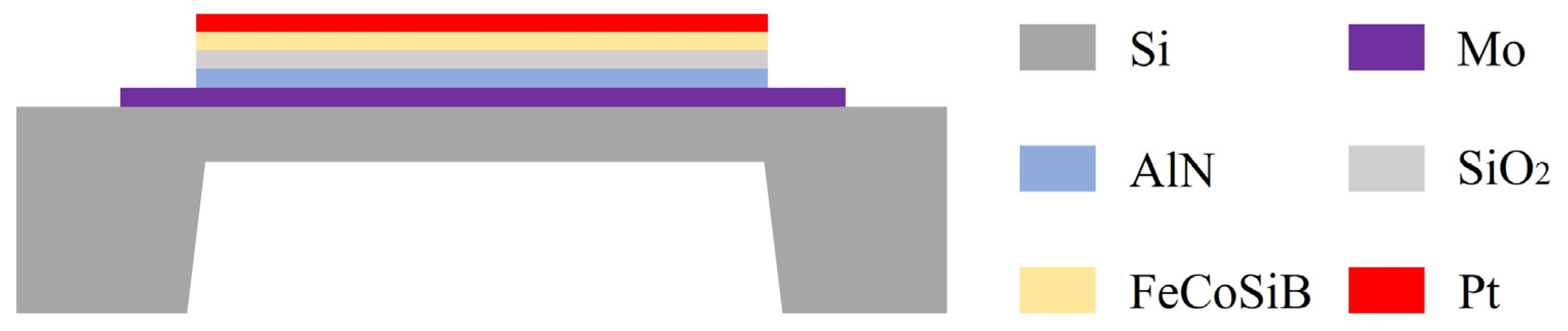
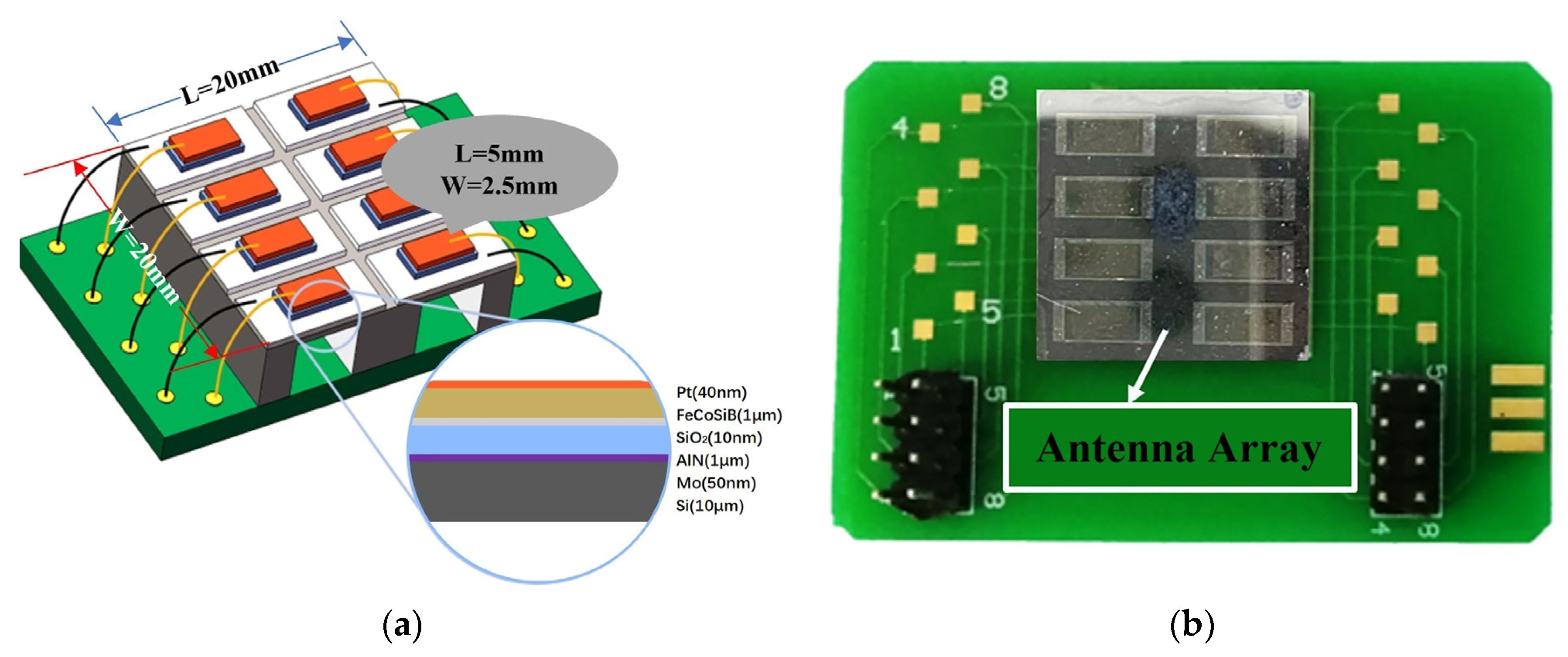
2. Structure and Fabrication
2.1. Materials
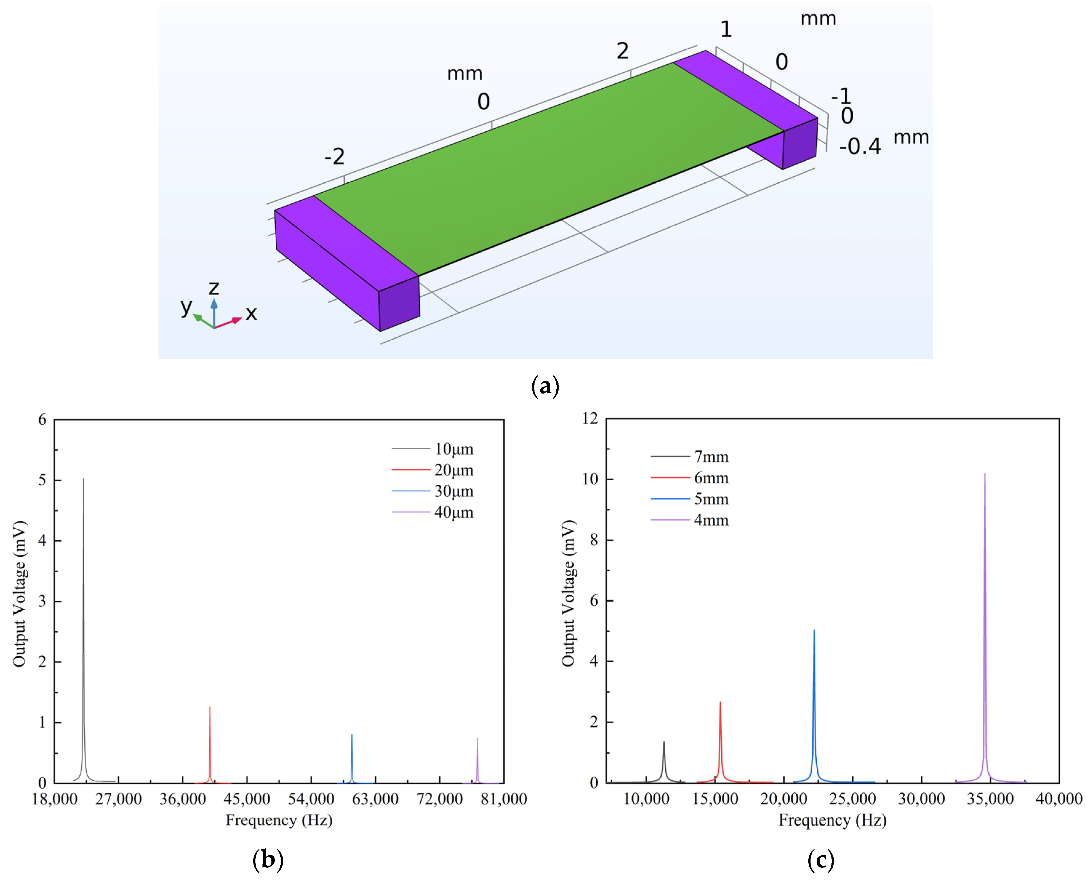
2.2. Simulation
2.3. Fabrication
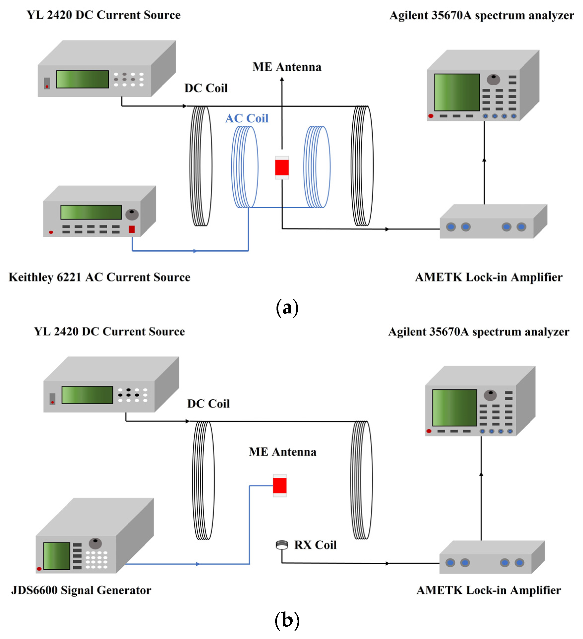
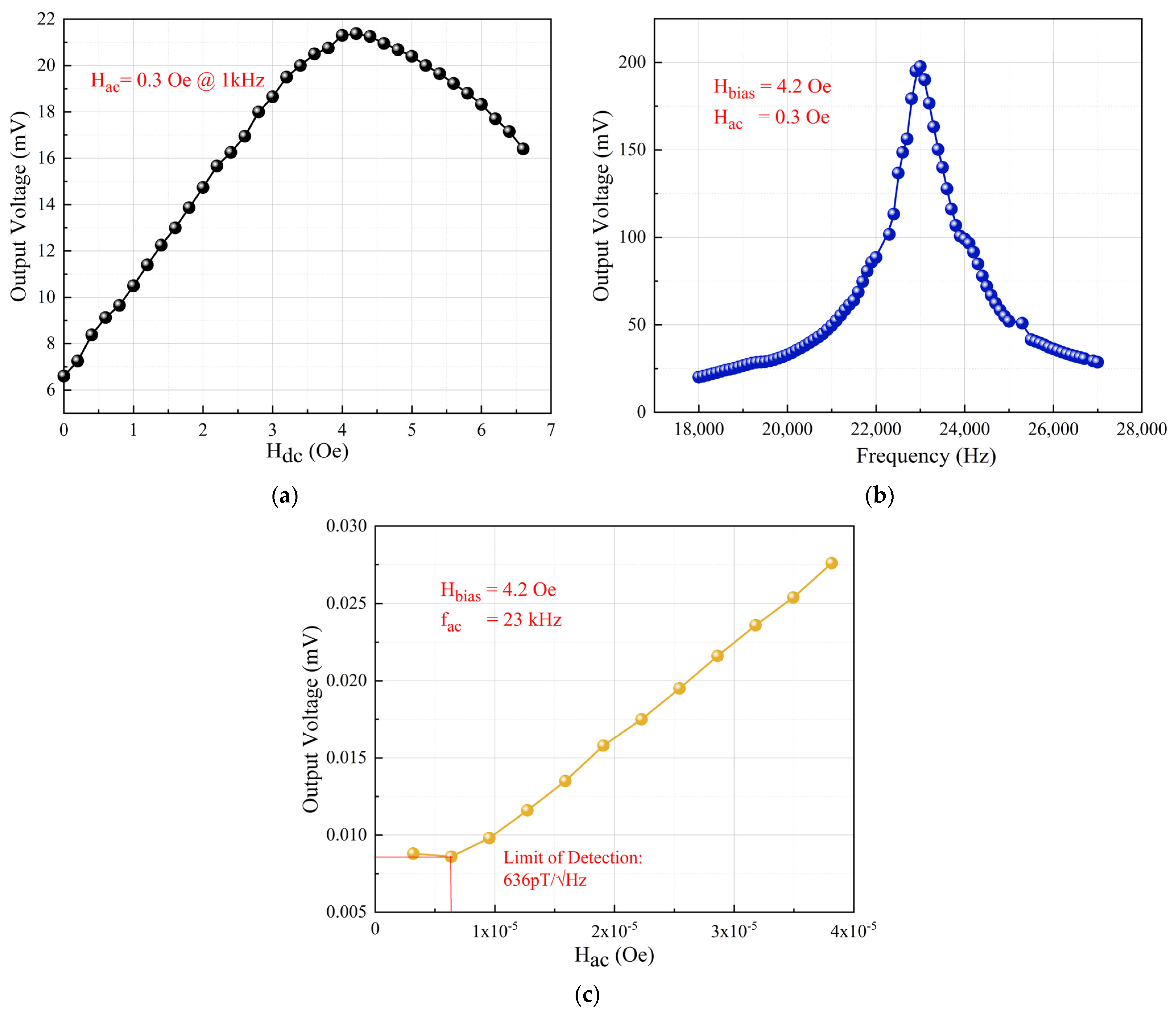
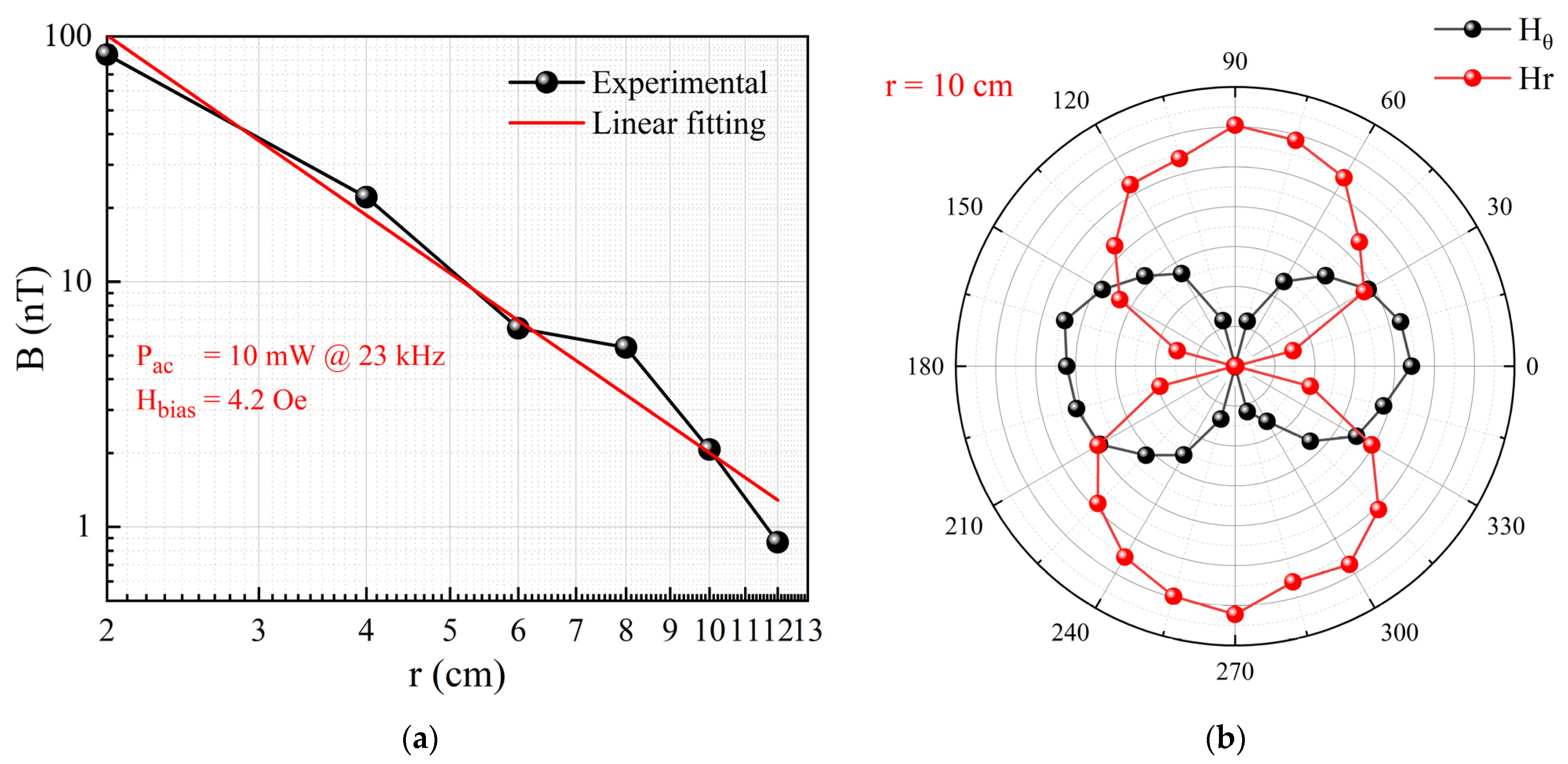
3. Experiments and Analysis
3.1. Performance of Single ME Antenna
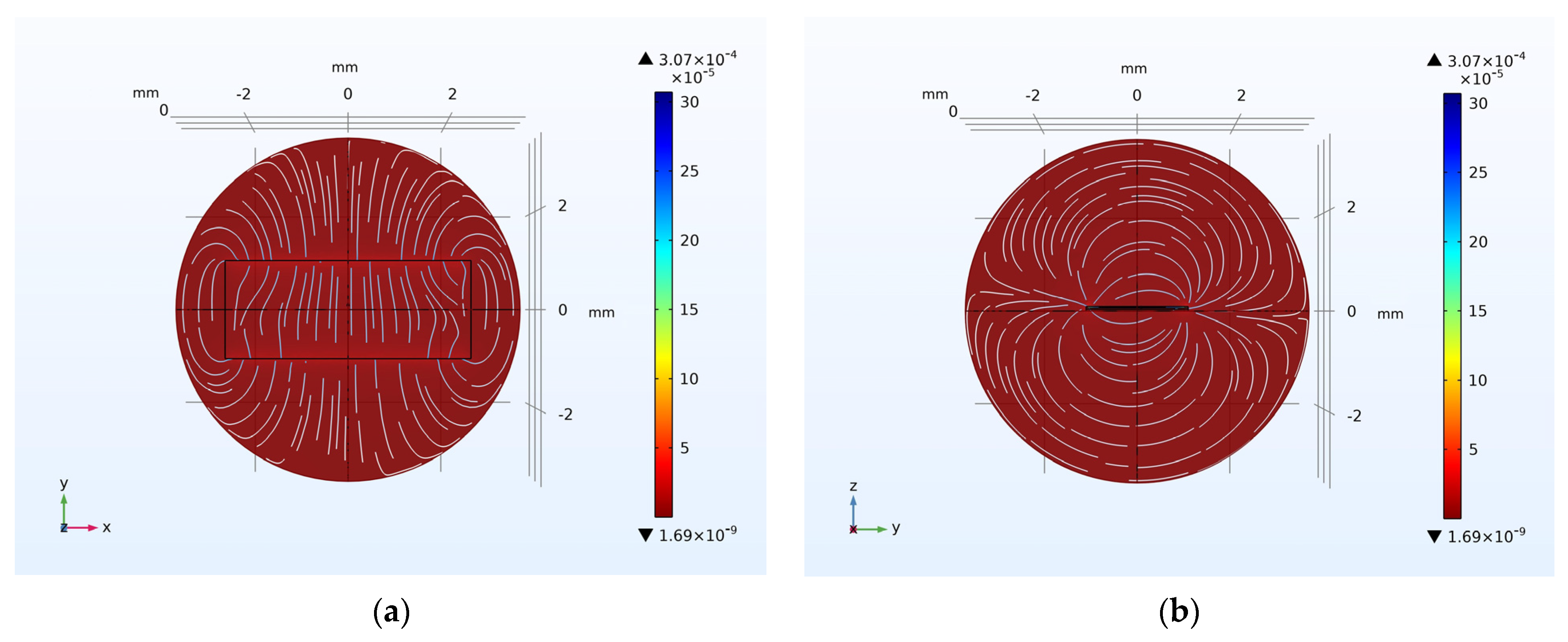
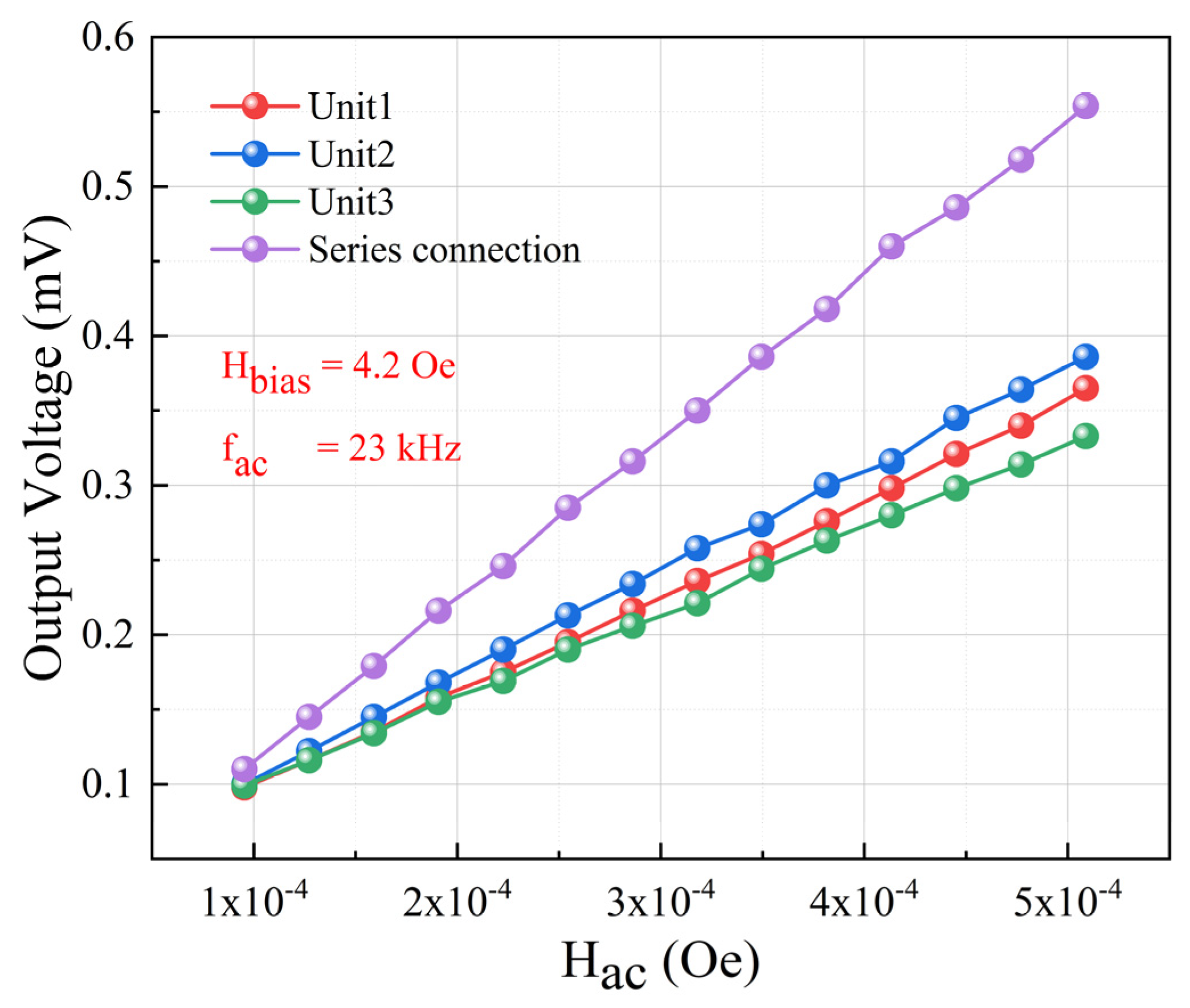
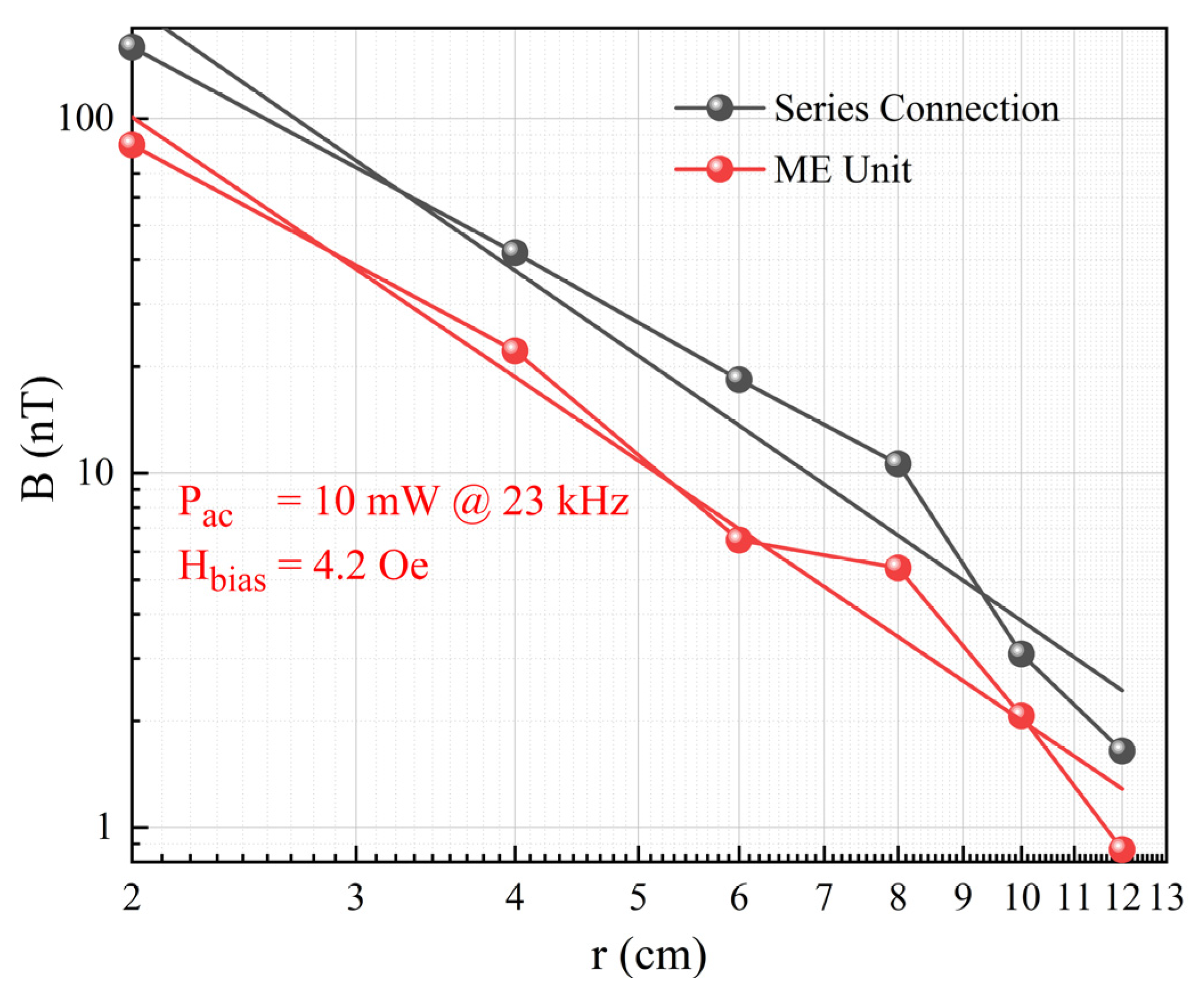
3.2. Performance of Series Connection
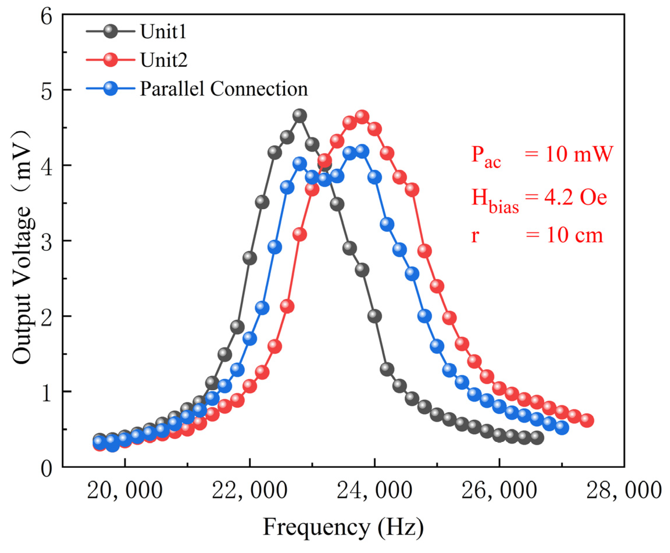
3.3. Performance of Parallel Connection
3.4. Comparison with Reported ME Antennas
4. Conclusions
Author Contributions
Funding
Data Availability Statement
Conflicts of Interest
References
- Chen, H.H.; Liang, X.F.; Dong, C.Z.; He, Y.F.; Sun, N.; Zaeimbashi, M.; He, Y.X.; Gao, Y.; Parimi, P.V.; Lin, H.; et al. Ultra-compact mechanical antennas. Appl. Phys. Lett. 2020, 117, 170501. [Google Scholar] [CrossRef]
- Yao, Z.; Wang, Y.E.; Keller, S.; Carman, G.P. Bulk Acoustic Wave-Mediated Multiferroic Antennas: Architecture and Performance Bound. IEEE Trans. Antennas Propag. 2015, 63, 3335–3344. [Google Scholar] [CrossRef]
- Lin, H.; Zaeimbashi, M.; Sun, N.; Liang, X.F.; Chen, H.H.; Dong, C.Z.; Matyushov, A.; Wang, X.J.; Guo, Y.X.; Gao, Y.; et al. Future antenna miniaturization mechanism: Magnetoelectric antennas. In Proceedings of the IEEE/MTT-S International Microwave Symposium, Philadelphia, PA, USA, 10–15 June 2018; pp. 220–223. [Google Scholar]
- Zaeimbashi, M.; Nasrollahpour, M.; Khalifa, A.; Romano, A.; Liang, X.F.; Chen, H.H.; Sun, N.; Matyushov, A.; Lin, H.; Dong, C.Z.; et al. Ultra-compact dual-band smart NEMS magnetoelectric antennas for simultaneous wireless energy harvesting and magnetic field sensing. Nat. Commun. 2021, 12, 3141. [Google Scholar] [CrossRef] [PubMed]
- Niu, Y.; Ren, H. A miniaturized low frequency (LF) magnetoelectric receiving antenna with an integrated DC magnetic bias. Appl. Phys. Lett. 2021, 118, 264104. [Google Scholar] [CrossRef]
- Nan, T.X.; Lin, H.; Gao, Y.; Matyushov, A.; Yu, G.L.; Chen, H.H.; Sun, N.; Wei, S.J.; Wang, Z.G.; Li, M.H.; et al. Acoustically actuated ultra-compact NEMS magnetoelectric antennas. Nat. Commun. 2017, 8, 296. [Google Scholar] [CrossRef] [PubMed]
- Xu, J.R.; Leung, C.M.; Zhuang, X.; Li, J.F.; Bhardwaj, S.; Volakis, J.; Viehland, D. A Low Frequency Mechanical Transmitter Based on Magnetoelectric Heterostructures Operated at Their Resonance Frequency. Sensors 2019, 19, 853. [Google Scholar] [CrossRef] [PubMed]
- Yao, Z.; Tiwari, S.; Lu, T.; Rivera, J.; Luong, K.Q.T.; Candler, R.N.; Carman, G.P.; Wang, Y.E. Modeling of Multiple Dynamics in the Radiation of Bulk Acoustic Wave Antennas. IEEE J. Multiscale Multiphys. Comput. Technol. 2020, 5, 5–18. [Google Scholar] [CrossRef]
- Dong, C.Z.; He, Y.F.; Li, M.H.; Tu, C.; Chu, Z.Q.; Liang, X.F.; Chen, H.H.; Wei, Y.Y.; Zaeimbashi, M.; Wang, X.J.; et al. A Portable Very Low Frequency (VLF) Communication System Based on Acoustically Actuated Magnetoelectric Antennas. IEEE Antennas Wirel. Propag. Lett. 2020, 19, 398–402. [Google Scholar] [CrossRef]
- Das, D.; Xu, Z.Y.; Nasrollahpour, M.; Martos-Repath, I.; Zaeimbashi, M.; Khalifa, A.; Mittal, A.; Cash, S.S.; Sun, N.X.; Shrivastava, A.; et al. Circuit-Level Modeling and Simulation of Wireless Sensing and Energy Harvesting with Hybrid Magnetoelectric Antennas for Implantable Neural Devices. IEEE Open J. Circuits Syst. 2023, 4, 139–155. [Google Scholar] [CrossRef]
- Cai, X.Y.; Zhang, K.H.; Zhao, T.X.; Yu, Z.T.; Liang, J.; Zhang, Y.H.; Wang, H.B.; Jin, H.; Dong, S.R.; Xuan, W.P.; et al. Finite Element Analysis and Optimization of Acoustically Actuated Magnetoelectric Microantennas. IEEE Trans. Antennas Propag. 2023, 71, 4640–4650. [Google Scholar] [CrossRef]
- Zhang, Y.; Jing, L.; Shi, P.; Hou, J.; Yang, X.; Peng, Y.; Chen, S. Research on a miniaturized VLF antenna array based on a magnetoelectric heterojunction. J. Mater. Sci. Mater. Electron. 2022, 33, 4211–4224. [Google Scholar] [CrossRef]
- Lin, H.; Zaeimbashi, M.; Sun, N.; Liang, X.F.; Chen, H.H.; Dong, C.Z.; Matyushov, A.; Wang, X.J.; Guo, Y.X.; Gao, Y.; et al. NEMS magnetoelectric antennas for biomedical application. In Proceedings of the IEEE/MTT-S International Microwave Biomedical Conference (IEEE-IMBioC), Philadelphia, PA, USA, 14–15 June 2018; pp. 13–15. [Google Scholar]
- Yun, X.F.; Lin, W.K.; Hu, R.; Liu, Y.Z.; Wang, X.Y.; Yu, G.H.; Zeng, Z.M.; Zhang, X.P.; Zhang, B.S. Bandwidth-enhanced magnetoelectric antenna based on composite bulk acoustic resonators. Appl. Phys. Lett. 2022, 121, 033501. [Google Scholar] [CrossRef]
- Zhuang, X.; Xu, X.; Zhang, X.; Sun, Y.; Yan, B.; Liu, L.S.; Lu, Y.T.; Zhu, W.H.; Fang, G.Y. Tailoring the magnetomechanical power efficiency of metallic glasses for magneto-electric devices. J. Appl. Phys. 2022, 132, 104502. [Google Scholar] [CrossRef]
- Dong, C.; He, Y.; Liu, X.; Sun, N.X. VLF mechanical antenna arrays for underwater wireless communications. In Proceedings of the 16th International Conference on Underwater Networks & Systems, Boston, MA, USA, 14–16 November 2022. Article 7. [Google Scholar]
- Dong, B.; Yan, Z.M.; Zhang, Y.; Han, T.H.; Zhou, H.C.; Wang, Y. Analysis of near field mutual coupling in wideband magnetoelectric antennas array. J. Appl. Phys. 2023, 134, 114103. [Google Scholar] [CrossRef]
- Liu, F.; Hashim, N.A.; Liu, Y.T.; Abed, M.R.M.; Li, K. Progress in the production and modification of PVDF membranes. J. Membr. Sci. 2011, 375, 1–27. [Google Scholar] [CrossRef]
- Chen, Y.; Bao, X.L.; Wong, C.M.; Cheng, J.; Wu, H.D.; Song, H.Z.; Ji, X.R.; Wu, S.H. PZT ceramics fabricated based on stereolithography for an ultrasound transducer array application. Ceram. Int. 2018, 44, 22725–22730. [Google Scholar] [CrossRef]
- Zhao, X.Q.; Shang, Z.G.; Luo, G.X.; Deng, L.C. A vibration energy harvester using AlN piezoelectric cantilever array. Microelectron. Eng. 2015, 142, 47–51. [Google Scholar] [CrossRef]
- Röbisch, V.; Salzer, S.; Urs, N.O.; Reermann, J.; Yarar, E.; Piorra, A.; Kirchhof, C.; Lage, E.; Höft, M.; Schmidt, G.U.; et al. Pushing the detection limit of thin film magnetoelectric heterostructures. J. Mater. Res. 2017, 32, 1009–1019. [Google Scholar] [CrossRef]
- Zhai, J.; Xing, Z.; Dong, S.; Li, J.; Viehland, D. Magnetoelectric laminate composites: An overview. J. Am. Ceram. Soc. 2008, 91, 351–358. [Google Scholar] [CrossRef]
- Torah, R.N.; Beeby, S.P.; White, N.M. Experimental investigation into the effect of substrate clamping on the piezoelectric behaviour of thick-film PZT elements. J. Phys. D-Appl. Phys. 2004, 37, 1074–1078. [Google Scholar] [CrossRef]
- Horsley, D.; Lu, Y.; Rozen, O. Flexural piezoelectric resonators. In Piezoelectric MEMS Resonators; Bhugra, H., Piazza, G., Eds.; Springer International Publishing: Cham, Switzerland, 2017; pp. 153–173. [Google Scholar]
- Mileham, J.R.; Pearton, S.J.; Abernathy, C.R.; MacKenzie, J.D.; Shul, R.J.; Kilcoyne, S.P. Wet chemical etching of AlN. Appl. Phys. Lett. 1995, 67, 1119–1121. [Google Scholar] [CrossRef]
- Cimalla, I.; Foerster, C.; Cimalla, V.; Lebedev, V.; Cengher, D.; Ambacher, O. Wet chemical etching of AIN in KOH solution. In Proceedings of the 6th International Conference on Nitride Semiconductors (ICNS-6), Bremen, Germany, 28 June–2 September 2005; pp. 1767–1770. [Google Scholar]
- Xing, Z.P.; Zhai, J.Y.; Gao, J.Q.; Li, J.F.; Viehland, D. Magnetic-Field Sensitivity Enhancement by Magnetoelectric Sensor Arrays. IEEE Electron Device Lett. 2009, 30, 445–447. [Google Scholar] [CrossRef]


| BaTiO3 | PZT | PMN-PT | AlN | PVDF | |
|---|---|---|---|---|---|
| d31 (pC/N) | −90 | −175 | ~700 | −2 | 16.5 |
| d33 (pC/N) | 191 | 400 | 2000 | 5.5 | −33 |
| ɛr | 1700 | 1750 | 5000 | 10.5 | 10 |
| ρ (g/cm3) | 6 | 7.7 | 7.8 | 3.3 | 1.78 |
| K33 | 0.63 | 0.72 | 0.9~0.94 | 0.24 | 0.19 |
| NiFe2O4 | Terfenol-D | Fe-Ga | Metglas2605 | FeCoSiB | |
|---|---|---|---|---|---|
| d33 (nm/A) | - | 25 | 20 | - | 50.3 |
| λS (ppm) | 27 | 1400 | 200 | 40 | 158 |
| μr | 20 | 6~10 | 20 | >40,000 | 70,000 |
| ρ (g/cm3) | 5.37 | 7.8 | 7.7 | 7.18 | 7.59 |
| K33 | - | 0.44 | - | 0.37 | - |
| ME Antenna Unit | Unit 1 | Unit 2 | Unit 3 | Series Connection |
|---|---|---|---|---|
| Capacitance (nF) | 8.456 | 8.247 | 8.024 | 4.581 |
| Reference | Center Frequency | Radiation Intensity | Relative Bandwidth | Size of a Single Unit | Composition |
|---|---|---|---|---|---|
| [7] | 28.1 kHz | 1 nT @ 1.35 m, 100 mW | - | 20 mm2 | PZT/Metglas |
| [12] | 26 kHz | 1.06 nT @ 1.2 m, 10 mW | 3.7% | 20 mm2 | PZT/Metglas |
| [16] | 23.7 kHz | 200 nT @ 1 m, - | 0.83% | 9 mm2 | PZT/Metglas |
| This work | 23 kHz | 3.1 nT @ 0.1 m, 10 mW | 9.6% | 2.5 mm2 | AlN/FeCoSiB |
Disclaimer/Publisher’s Note: The statements, opinions and data contained in all publications are solely those of the individual author(s) and contributor(s) and not of MDPI and/or the editor(s). MDPI and/or the editor(s) disclaim responsibility for any injury to people or property resulting from any ideas, methods, instructions or products referred to in the content. |
© 2023 by the authors. Licensee MDPI, Basel, Switzerland. This article is an open access article distributed under the terms and conditions of the Creative Commons Attribution (CC BY) license (https://creativecommons.org/licenses/by/4.0/).
Share and Cite
Jin, J.; Jing, L.; Zuo, C.; Ma, Z.; Shi, Y.; Yang, X.; Chen, S. Array Study of VLF Thin-Film Magnetoelectric Antenna with a Microbridge Structure. Micromachines 2024, 15, 11. https://doi.org/10.3390/mi15010011
Jin J, Jing L, Zuo C, Ma Z, Shi Y, Yang X, Chen S. Array Study of VLF Thin-Film Magnetoelectric Antenna with a Microbridge Structure. Micromachines. 2024; 15(1):11. https://doi.org/10.3390/mi15010011
Chicago/Turabian StyleJin, Jianhua, Long Jing, Chao Zuo, Zhiling Ma, Yanfeng Shi, Xiaofei Yang, and Shi Chen. 2024. "Array Study of VLF Thin-Film Magnetoelectric Antenna with a Microbridge Structure" Micromachines 15, no. 1: 11. https://doi.org/10.3390/mi15010011
APA StyleJin, J., Jing, L., Zuo, C., Ma, Z., Shi, Y., Yang, X., & Chen, S. (2024). Array Study of VLF Thin-Film Magnetoelectric Antenna with a Microbridge Structure. Micromachines, 15(1), 11. https://doi.org/10.3390/mi15010011