Abstract
Oxygen vacancies are a major factor that controls the electrical characteristics of the amorphous indium-gallium-zinc oxide transistor (a-IGZO TFT). Oxygen vacancies are affected by the composition ratio of the a-IGZO target and the injected oxygen flow rate. In this study, we fabricated three types of a-IGZO TFTs with different oxygen flow rates and then investigated changes in electrical characteristics. Atomic force microscopy (AFM) was performed to analyze the surface morphology of the a-IGZO films according to the oxygen gas rate. Furthermore, X-ray photoelectron spectroscopy (XPS) analysis was performed to confirm changes in oxygen vacancies of a-IGZO films. The optimized a-IGZO TFT has enhanced electrical characteristics such as carrier mobility (μ) of 12.3 cm2/V·s, on/off ratio of 1.25 × 10¹⁰ A/A, subthreshold swing (S.S.) of 3.7 V/dec, and turn-on voltage (Vto) of −3 V. As a result, the optimized a-IGZO TFT has improved electrical characteristics with oxygen vacancies having the highest conductivity.
1. Introduction
Since 2004, when Hideo Hosono presented an amorphous indium gallium zinc oxide (a-IGZO) and its use in transparent and flexible thin-film TFTs (TFTs), a-IGZO-based TFTs have drawn considerable attention [1,2,3]. In particular, a-IGZO-based TFTs are currently used in the display industry as this device offers high carrier mobility and, accordingly, sufficient driving current density to operate an organic light-emitting diode (OLED) can be made available [4,5,6]. Furthermore, another merit of a-IGZO-based TFTs is large-area deposition with high uniformity [7,8,9]. Due to these merits, many efforts have been made to implement a new concept of electronic devices such as neuromorphic devices [10,11,12], gas sensors [13,14,15], photodetectors [16,17,18], biosensors [19,20,21], and logic circuits [22,23,24].
One of the most frequently used deposition methods for a-IGZO is sputtering. This deposition method provides a facile deposition of thin films, particularly oxides, by means of sputtering from a “target” source to a “substrate” [25,26,27]. As oxygen vacancy concentration in a-IGZO significantly determines the electrical properties of TFTs, specific deposition conditions, including gas flow rate dependency, should be considered [28], and thus, its optimization should be accompanied.
In addition, annealing processes of metal oxide semiconductors (MOS) are improving carrier mobility [29,30,31]. Oxygen vacancy generated in MOS crystallized through the annealing process are important factors determining conductivity [32,33]. The oxygen vacancy behaves as an electron donor through a fully occupied defect state. Therefore, the conductivity of MOS increases due to the closer Fermi level and conduction band [34,35]. Compared to chemical doping methods and new designs of MOS-based devices, the annealing process provides a simple method and immediate effect for controlling the electrical characteristics of MOS. However, the high annealing temperature of over 600 °C and the additional pre-processing variables reduce the process compatibility of MOS-based devices [36,37,38].
Here, we investigate the a-IGZO TFT process conditions by controlling the oxygen flow rate without an additional annealing process. The effect of oxygen vacancies controlled by the oxygen gas rate was investigated using atomic force microscopy (AFM) and X-ray photoelectron spectroscopy (XPS) analysis. The a-IGZO TFT fabricated under optimized process conditions exhibits excellent electrical characteristics due to increased conductivity with oxygen vacancies. The carrier mobility and on/off ratio of the optimized a-IGZO TFT are 12.3 cm2/V·s and 1.25 × 10¹⁰ A/A, respectively. Also, the subthreshold swing (S.S.) of 3.7 V/dec and a Vto of −3 V were achieved.
2. Materials and Methods
To fabricate the a-IGZO TFTs, a heavily boron-doped p-type Si/SiO2 (300 nm) was prepared. The SiO2 layer was used as the gate dielectric, and a p-type Si layer was applied as the back gate. The Si/SiO2 wafer was cleaned with acetone and isopropyl alcohol and then dried with nitrogen gas. a-IGZO (In2O3: Ga2O3: ZnO = 1:1:1) for the channel of TFTs was deposited using the radio frequency (RF) magnetron sputtering method. Condition 1 (C1) is the deposition method of a-IGZO using only the Ar gas. The gas mixing ratio of O2:Ar injected during the deposition of a-IGZO is 1.7:100 (Condition 2, C2) and 17:100 (Condition 3, C3). The Ti (60 nm) source and drain electrode had deposited electron-beam evaporation. The width (W) and length (L) of the channels are 100 μm and 1000 μm, respectively. Figure 1a shows the channel and electrode patterning process of a-IGZO TFT using a shadow mask. Figure 1b shows a top-view optical microscope (OM) image of the a-IGZO TFT array. Also, Figure 1c shows the cross-sectional view image of a-IGZO TFT with a scanning electron microscope (SEM), and the thickness of optimized a-IGZO is 8 nm.
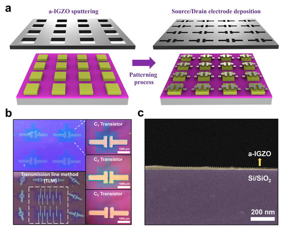
Figure 1.
(a) 3D schematic of channel and electrode patterning process of a-IGZO TFT using shadow mask. (b) Optical microscope image of a-IGZO TFT array according to a-IGZO sputtering conditions. (c) Scanning electron microscope image of a-IGZO TFT deposited under optimized process conditions.
The electrical characteristics of a-IGZO TFT were analyzed using a Keithley 4200 (Tektronix, Beaverton, OR, USA) semiconductor parameter analyzer in the air. The electrical characteristics of a-IGZO TFT were investigated according to oxygen gas injection conditions. Atomic force microscopy (AFM) images were measured by XE7 (Park Systems, Suwon, Republic of Korea). X-ray photoelectron spectroscopy (XPS) was measured using AXIS-SUPRA (Kratos, Manchester, UK) at the Korea Basic Science Institute (KBSI). The field-effect mobility and the subthreshold swing (S.S.) of TFTs were calculated using the equation:
where L and W represent the length and width of the channel, and C is the capacitance of the gate insulator. The VGS is the applied gate–source voltage, and ID is the drain current.
Also, the interface trap density (Dit) of the TFT was derived using the following equation [39]:
where q and T represent the elementary electron charge and absolute temperature, respectively. The KB is the Boltzmann constant, and e is the dielectric constant.
3. Results
Various variables, such as the atomic composition ratio of the a-IGZO target, O2/Ar mixed gas ratio, and thin film thickness, affect the electrical characteristics of a-IGZO TFTs. In particular, oxygen vacancies are essential due to controlling the electrical characteristics of a-IGZO TFTs. Moreover, oxygen vacancies on the surface of a-IGZO are affected by oxygen gas flow rates. For this reason, we fabricated three types of TFTs with different oxygen gas flow rates to investigate changes in electrical characteristics. Figure 2a shows the transfer curve of the C1 TFT fabricated under the optimized process conditions. The channel of the C1 TFT was deposited without oxygen gas injection. The gate–source voltage of the measured transfer curve was −30 V to 60 V, and a drain voltage of 10 V was applied. The on-current and off-current of the C1 TFT were measured to 6 × 10⁻⁴ A and 4.8 × 10⁻¹⁴ A, respectively, and the calculated on/off ratio was measured to as high as 1.25 × 10¹⁰ A/A. Figure 2b shows the output curve of the C1 TFT presenting conventional n-type operation. To measure the output curve, a range of the gate–source voltage is 0 V to 60 V and a drain voltage of 0 V to 50 V were applied, respectively. The contact resistance of a-IGZO TFT was evaluated using the transmission line method (TLM) method. As shown in Figure 2c, the extracted contact resistance is 0.4 Ω·cm using the TLM method. The contact resistance is related to charge injection, which affects electrical characteristics such as mobility and on/off ratio [40,41,42]. Therefore, the reduced contact resistance promotes charge injection to the channel, and the C1 TFT had improved mobility and on/off ratio performance. Figure 2d shows the transfer curves with three types of a-IGZO TFTs in different oxygen gas flow rates. The O2/Ar mixed gas ratios of the C2 and C3 TFTs are 1.7:100 and 17:100, respectively. The on-current of the a-IGZO TFT decreases as the oxygen flow rate increases. The electrical characteristics of the optimized a-IGZO TFT depend on the composition ratio of the a-IGZO target. The low conductivity of a-IGZO TFT fabricated with no oxygen component a-IGZO target is overcome by injecting the oxygen gas [43]. On the other hand, the a-IGZO TFT deposited by injecting additional oxygen gas into the a-IGZO target with an oxygen component has reduced oxygen vacancies, resulting in low conductivity. The on-currents at VGS = 60 V of the C1 and C2 TFTs were measured to 4.7 × 10⁻⁶ A and 6 × 10⁻⁴ A, respectively. The C2 TFT has 127 times less on-current compared to the C1 TFT. Therefore, the on/off ratio of the C2 TFT was 1.24 × 10⁶ A/A, which was decreased compared to that of the C1 TFT. The C3 TFT had reduced oxygen vacancy compared to C1 and C2 TFTs by injecting the highest amount of oxygen gas during a-IGZO sputtering. The low conductivity of the C3 TFT is attributed to the reduced carrier density due to excessive oxygen vacancy. Therefore, the C3 TFT has an average current of 67 pA in the gate–source voltage and ranges from −30 V to 60 V and could not be converted to on-state by the positive gate–source bias voltage.
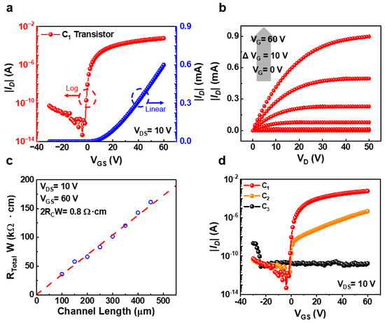
Figure 2.
(a) Transfer curve of optimized C1 TFT. (b) Output curve of optimized C1 TFT. (c) Contact resistance of optimized C1 TFT. (d) Device electrical characteristics according to oxygen flow variation.
The electrical parameters with the three types of a-IGZO TFTs were compared (Figure 3a–d). The electrical parameters include carrier mobility (μ), turn-on voltage (Vto), subthreshold swing (S.S.), and on/off ratio. The electrical parameters of the C3 TFT were uncalculated due to insufficient switching behavior due to the low conductivity of a-IGZO. The carrier mobility of the C1 TFT and C2 TFT is 12.3 cm2/V·s and 0.58 cm2/V·s, respectively. The carrier mobility of the C1 TFT is 21 times higher than that of the C2 TFT. Also, the Vto is −3 V and −5 V, respectively, and S.S. is 3.7 V/dec and 4.9 V/dec, respectively. As a result, the optimized C1 TFT achieved a high on/off ratio and carrier mobility. In addition, the electrical characteristics of C1 transistors with Vto close to zero gate–source voltage and low S.S. potentially enable low voltage operation and low power consumption. The high electron mobility and reduced S.S. of C1 TFT compared to C2 TFT are achieved due to the reduced oxygen vacancy and interface trap density (Dit) in a-IGZO. The extracted Dit of the C1 TFT and C2 TFT was 4.4 × 1012 cm−2 eV−1 and 5.8 × 1012 cm−2 eV−1, respectively. Appropriate oxygen vacancy and interface trap density minimize the trapping of charge carriers in C1 TFT, thereby increasing charge carrier mobility. Also, they decrease the S.S., inducing clear switching behavior of a-IGZO TFT [44,45,46]. Therefore, optimizing oxygen vacancy and interface trap density is crucial for improving the performance of a-IGZO TFTs, leading to enhanced charge carrier mobility and reduced S.S.
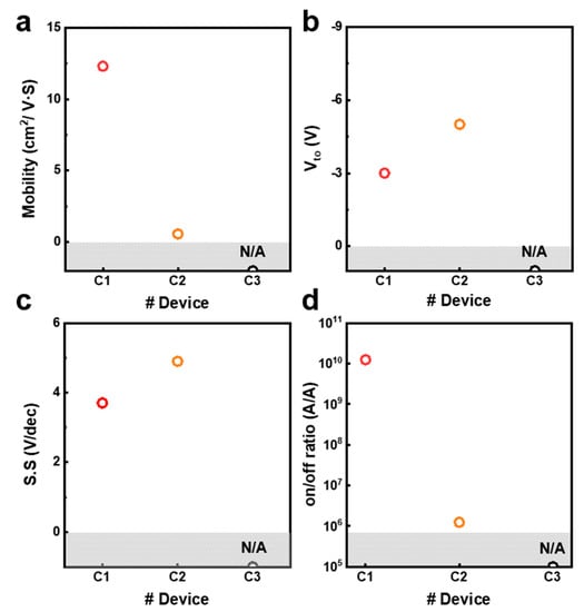
Figure 3.
Parameters in three types of a-IGZO TFTs. (a) Carrier mobility (μ). (b) Turn-on voltage (Vto). (c) Subthreshold swing (S.S). (d) On/off ratio.
Next, we performed an atomic force microscope (AFM) analysis to investigate the morphological characteristics of a-IGZO films fabricated by oxygen flow rate. Figure 4a–c shows the AFM image (5 μM × 5 μM) and height information of a-IGZO films using fabrication methods with C1, C2, and C3, respectively. The height information of the a-IGZO surface did not become rough when oxygen gas flow was increased [47,48]. The morphological characteristics changes on the surface of a-IGZO are related to the concentration of oxygen vacancy. The defect, such as oxygen vacancy, induces rough surface morphology of a-IGZO films. As a result, a high concentration of oxygen vacancy causes the surface of a-IGZO morphology to be rough, while a low concentration of oxygen vacancy induces a smoother surface morphology [31,49]. In addition, the average roughness (Ra) and root mean square roughness (Rq) were calculated from the height information of a-IGZO using the AFM measurement (Figure 4d). The Ra value of C1, C2, and C3 was 0.134, 0.111, and 0.089 nm, respectively. In addition, the values of Rq are 0.151, 0.134, and 0.126 nm, increasing with the oxygen flow rate.
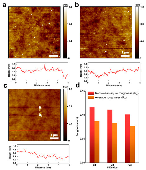
Figure 4.
Atomic force microscopy (AFM) image and height information for morphology analysis (a) C1 TFT. (b) C2 TFT. (c) C3 TFT. (d) Average roughness (Ra) and root mean square roughness (Rq) of three IGZO films with different oxygen flow rates.
To investigate the chemical composition difference between the three types of a-IGZO films, X-ray photoelectron spectroscopy (XPS) analysis was performed. Figure 5a–c shows the O 1s spectra of the a-IGZO films according to the oxygen gas flow during deposition. The O 1s spectra of the a-IGZO are separated into sub-peaks associated with O2- ions, such as metal-oxide (M-O) bonds, metal-hydroxyl (M-OH) bonds, and oxygen vacancies. The sub-peaks of O 1s indicate binding at 530 eV, 532 eV, and 531 eV, respectively. The M-O bonds (530 eV) are formed by bonding O2- ions with elements of a-IGZO metals such as indium, gallium, and zinc. Also, the M-OH bonds (532 eV) were referred between the metals of a-IGZO and the hydroxyl group. In addition, the oxygen vacancies (531 eV) are defects of the a-IGZO channels, which were generated by oxygen atoms and are related to the carrier concentration of a-IGZO. The oxygen gas injected during sputtering reduced the oxygen vacancies of the deposited a-IGZO film. The relative areas of oxygen vacancies in C1, C2, and C3 were 30.6%, 29.6%, and 27.4%, respectively, which oxygen vacancies are reduced when injected oxygen gas was increased. The oxygen vacancy is known to have a significant effect on the change of electrical characteristics in a-IGZO thin firm TFTs [50]. Adequate oxygen vacancies increase the conductivity of a-IGZO by generating free electrons [51]. In addition, the M-OH bond of a-IGZO was decreased as the oxygen flow rate increased [52]. The relative area of M-OH bond in C1, C2, and C3 were 9.5%, 9%, and 4.95%, respectively. The M-OH bond acts as a deep-level trap that prevents charge transport in the a-IGZO, inducing the operation of the unstable TFT [53]. As a result, the optimized C1 TFT has improved electrical characteristics due to adequate oxygen vacancies and reduced M-OH bonding.
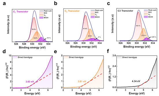
Figure 5.
The O 1s peak of XPS spectra in a-IGZO films (a) a-IGZO films deposited in C1. (b) a-IGZO films deposited in C2. (c) a-IGZO films deposited in C3. Optical bandgap of a-IGZO films using Tauc plot method (d) a-IGZO films deposited in C1. (e) a-IGZO films deposited in C2. (f) a-IGZO films deposited in C3.
Moreover, the changes in the optical bandgap of a-IGZO with oxygen gas flow were investigated. Figure 5d–f shows the optical bandgap of a-IGZO calculated by the Tauc plot method using UV–visible absorption data. The a-IGZO in the C1 condition without oxygen injection showed the smallest optical bandgap of 3.63 eV. On the other hand, the optical bandgaps of C2 and C3 increased by oxygen injection are 3.81 eV and 4.34 eV, respectively. As a result, the optical bandgap of a-IGZO was increased as the injected oxygen gas was increased.
4. Conclusions
In summary, the electrical characteristics of oxygen flow rate injection were investigated. As a result, when oxygen flow rate injection was not performed, the best electrical characteristics such as mobility, Vto, and on/off ratio were shown. The decreased oxygen vacancy in a-IGZO caused by an increased oxygen gas flow rate results in a decreased conductivity. The C1 TFT without oxygen gas injected has enhanced charge carrier mobility due to high oxygen vacancy. In addition, AFM and XPS analyses were performed to confirm the mechanism of the change in electrical properties due to oxygen flow injection. In the AFM analysis, the improvement of electrical properties was confirmed through wide contact with the electrode material because the C1 device had the greatest roughness. Finally, through XPS analysis, it was confirmed that the electrical characteristics of the C1 device with the highest oxygen vacancy were the best. Through this result, we believe that the development of oxide semiconductor research and process condition research will be inexhaustible.
Author Contributions
H.Y. contributed to the conceptualization of this research. Y.H. and D.H.L. performed the experiments and analysis and wrote the original manuscript. E.-S.C., S.J.K. and H.Y. reviewed and edited the manuscript. All authors have read and agreed to the published version of the manuscript.
Funding
This work was supported in part by the Korea Institute for Advancement of Technology (KIAT) grant funded by the Korean Government (MOTIE) (No. P0012453, The Competency Development Program for Industry Specialist) and partly supported by the National Research Foundation of Korea (NRF) grant funded by the Korean government (MSIT) (No. NRF-2022R1A2C1003076). This work was supported in part by the Technology Innovation Program (00144300, Interface Technology of 3D Stacked Heterogeneous System for SCM-based Process-in-Memory) funded by the Ministry of Trade, Industry and Energy (MOTIE, Korea).
Conflicts of Interest
The authors declare no conflict of interest.
References
- Nomura, K.; Ohta, H.; Takagi, A.; Kamiya, T.; Hirano, M.; Hosono, H. Room-Temperature Fabrication of Transparent Flexible Thin-Film Transistors Using Amorphous Oxide Semiconductors. Nature 2004, 432, 488–492. [Google Scholar] [CrossRef] [PubMed]
- Li, X.; Geng, D.; Mativenga, M.; Jang, J. High-Speed Dual-Gate a-IGZO TFT-Based Circuits with Top-Gate Offset Structure. IEEE Electron. Device Lett. 2014, 35, 461–463. [Google Scholar] [CrossRef]
- Rahaman, A.; Chen, Y.; Hasan, M.M.; Jang, J. A High Performance Operational Amplifier Using Coplanar Dual Gate A-IGZO TFTs. IEEE J. Electron. Devices Soc. 2019, 7, 655–661. [Google Scholar] [CrossRef]
- Park, Y.; Cho, D.Y.; Kim, R.; Kim, K.H.; Lee, J.W.; Lee, D.H.; Jeong, S.I.; Ahn, N.R.; Lee, W.; Choi, J.B. Defect Engineering for High Performance and Extremely Reliable A-IGZO Thin-Film Transistor in QD-OLED. Adv. Electron. Mater. 2022, 8, 2101273. [Google Scholar] [CrossRef]
- Sodhani, A.; Kandpal, K. Design of Threshold Voltage Insensitive Pixel Driver Circuitry Using A-IGZO TFT for AMOLED Displays. Microelectron. J. 2020, 101, 104819. [Google Scholar] [CrossRef]
- Kim, D.; Kim, Y.; Lee, S.; Kang, M.S.; Kim, D.H.; Lee, H. High Resolution A-IGZO TFT Pixel Circuit for Compensating Threshold Voltage Shifts and OLED Degradations. IEEE J. Electron. Devices Soc. 2017, 5, 372–377. [Google Scholar] [CrossRef]
- Lin, C.-L.; Chang, W.-Y.; Hung, C.-C. Compensating Pixel Circuit Driving AMOLED Display with A-IGZO TFTs. IEEE Electron. Device Lett. 2013, 34, 1166–1168. [Google Scholar] [CrossRef]
- Kim, J.-S.; Byun, J.-W.; Jang, J.-H.; Kim, Y.-D.; Han, K.-L.; Park, J.-S.; Choi, B.-D. A High-Reliability Carry-Free Gate Driver for Flexible Displays Using a-IGZO TFTs. IEEE Trans. Electron. Devices 2018, 65, 3269–3276. [Google Scholar] [CrossRef]
- Lee, G.J.; Kim, J.; Kim, J.-H.; Jeong, S.M.; Jang, J.E.; Jeong, J. High Performance, Transparent a-IGZO TFTs on a Flexible Thin Glass Substrate. Semicond. Sci. Technol. 2014, 29, 35003. [Google Scholar] [CrossRef]
- Kwon, S.M.; Cho, S.W.; Kim, M.; Heo, J.S.; Kim, Y.; Park, S.K. Environment-adaptable Artificial Visual Perception Behaviors Using a Light-adjustable Optoelectronic Neuromorphic Device Array. Adv. Mater. 2019, 31, 1906433. [Google Scholar] [CrossRef]
- Yang, Y.; He, Y.; Nie, S.; Shi, Y.; Wan, Q. Light Stimulated IGZO-Based Electric-Double-Layer Transistors for Photoelectric Neuromorphic Devices. IEEE Electron. Device Lett. 2018, 39, 897–900. [Google Scholar] [CrossRef]
- Jang, Y.; Park, J.; Kang, J.; Lee, S.-Y. Amorphous InGaZnO (a-IGZO) Synaptic Transistor for Neuromorphic Computing. ACS Appl. Electron. Mater. 2022, 4, 1427–1448. [Google Scholar] [CrossRef]
- Yang, D.J.; Whitfield, G.C.; Cho, N.G.; Cho, P.-S.; Kim, I.-D.; Saltsburg, H.M.; Tuller, H.L. Amorphous InGaZnO4 Films: Gas Sensor Response and Stability. Sens. Actuators B Chem. 2012, 171, 1166–1171. [Google Scholar] [CrossRef]
- Chen, P.-L.; Liu, I.-P.; Chen, W.-C.; Niu, J.-S.; Liu, W.-C. Study of a Platinum Nanoparticle (Pt NP)/Amorphous In-Ga-Zn-O (A-IGZO) Thin-Film-Based Ammonia Gas Sensor. Sens. Actuators B Chem. 2020, 322, 128592. [Google Scholar] [CrossRef]
- Zan, H.-W.; Li, C.-H.; Yeh, C.-C.; Dai, M.-Z.; Meng, H.-F.; Tsai, C.-C. Room-Temperature-Operated Sensitive Hybrid Gas Sensor Based on Amorphous Indium Gallium Zinc Oxide Thin-Film Transistors. Appl. Phys. Lett. 2011, 98, 253503. [Google Scholar] [CrossRef]
- Zhang, Y.Y.; Qian, L.X.; Lai, P.T.; Dai, T.J.; Liu, X.Z. Improved Detectivity of Flexible A-InGaZnO UV Photodetector via Surface Fluorine Plasma Treatment. IEEE Electron. Device Lett. 2019, 40, 1646–1649. [Google Scholar] [CrossRef]
- Yamada, N.; Kondo, Y.; Cao, X.; Nakano, Y. Visible-Blind Wide-Dynamic-Range Fast-Response Self-Powered Ultraviolet Photodetector Based on CuI/In-Ga-Zn-O Heterojunction. Appl. Mater. Today 2019, 15, 153–162. [Google Scholar] [CrossRef]
- Huang, C.-Y.; Peng, T.-Y.; Hsieh, W.-T. Realization of a Self-Powered InGaZnO MSM UV Photodetector Using Localized Surface Fluorine Plasma Treatment. ACS Appl. Electron. Mater. 2020, 2, 2976–2983. [Google Scholar] [CrossRef]
- Lee, I.-K.; Lee, K.H.; Lee, S.; Cho, W.-J. Microwave Annealing Effect for Highly Reliable Biosensor: Dual-Gate Ion-Sensitive Field-Effect Transistor Using Amorphous InGaZnO Thin-Film Transistor. ACS Appl. Mater. Interfaces 2014, 6, 22680–22686. [Google Scholar] [CrossRef] [PubMed]
- Son, H.W.; Park, J.H.; Chae, M.-S.; Kim, B.-H.; Kim, T.G. Bilayer Indium Gallium Zinc Oxide Electrolyte-Gated Field-Effect Transistor for Biosensor Platform with High Reliability. Sens. Actuators B Chem. 2020, 312, 127955. [Google Scholar] [CrossRef]
- Bhatt, D.; Kumar, S.; Panda, S. Amorphous IGZO Field Effect Transistor Based Flexible Chemical and Biosensors for Label Free Detection. Flex. Print. Electron. 2020, 5, 14010. [Google Scholar] [CrossRef]
- Seok, M.J.; Choi, M.H.; Mativenga, M.; Geng, D.; Kim, D.Y.; Jang, J. A Full-Swing a-IGZO TFT-Based Inverter with a Top-Gate-Bias-Induced Depletion Load. IEEE Electron. Device Lett. 2011, 32, 1089–1091. [Google Scholar] [CrossRef]
- Cho, I.-T.; Lee, J.-W.; Park, J.-M.; Cheong, W.-S.; Hwang, C.-S.; Kwak, J.-S.; Cho, I.-H.; Kwon, H.-I.; Shin, H.; Park, B.-G. Full-Swing a-IGZO Inverter with a Depletion Load Using Negative Bias Instability under Light Illumination. IEEE Electron. Device Lett. 2012, 33, 1726–1728. [Google Scholar] [CrossRef]
- Kim, J.-S.; Jang, J.-H.; Kim, Y.-D.; Byun, J.-W.; Han, K.; Park, J.-S.; Choi, B.-D. Dynamic Logic Circuits Using A-IGZO TFTs. IEEE Trans. Electron. Devices 2017, 64, 4123–4130. [Google Scholar] [CrossRef]
- Cho, M.H.; Seol, H.; Song, A.; Choi, S.; Song, Y.; Yun, P.S.; Chung, K.-B.; Bae, J.U.; Park, K.-S.; Jeong, J.K. Comparative Study on Performance of IGZO Transistors with Sputtered and Atomic Layer Deposited Channel Layer. IEEE Trans. Electron. Devices 2019, 66, 1783–1788. [Google Scholar] [CrossRef]
- Yao, R.; Zheng, Z.; Xiong, M.; Zhang, X.; Li, X.; Ning, H.; Fang, Z.; Xie, W.; Lu, X.; Peng, J. Low-Temperature Fabrication of Sputtered High-k HfO2 Gate Dielectric for Flexible a-IGZO Thin Film Transistors. Appl. Phys. Lett. 2018, 112, 103503. [Google Scholar] [CrossRef]
- Yao, R.; Zheng, Z.; Fang, Z.; Zhang, H.; Zhang, X.; Ning, H.; Wang, L.; Peng, J.; Xie, W.; Lu, X. High-Performance Flexible Oxide TFTs: Optimization of a-IGZO Film by Modulating the Voltage Waveform of Pulse DC Magnetron Sputtering without Post Treatment. J. Mater. Chem. C Mater. 2018, 6, 2522–2532. [Google Scholar] [CrossRef]
- Choi, H.-W.; Song, K.-W.; Kim, S.-H.; Nguyen, K.T.; Eadi, S.B.; Kwon, H.-M.; Lee, H.-D. Zinc Oxide and Indium-Gallium-Zinc-Oxide Bi-Layer Synaptic Device with Highly Linear Long-Term Potentiation and Depression Characteristics. Sci. Rep. 2022, 12, 1259. [Google Scholar] [CrossRef]
- Hwang, S.; Lee, J.H.; Woo, C.H.; Lee, J.Y.; Cho, H.K. Effect of Annealing Temperature on the Electrical Performances of Solution-Processed InGaZnO Thin Film Transistors. Thin Solid. Film. 2011, 519, 5146–5149. [Google Scholar] [CrossRef]
- Lin, C.-I.; Yen, T.-W.; Lin, H.-C.; Huang, T.-Y.; Lee, Y.-S. Effect of Annealing Ambient on the Characteristics of A-IGZO Thin Film Transistors. In Proceedings of the 4th IEEE International NanoElectronics Conference, Taoyuan, Taiwan, 21–24 June 2011; pp. 1–2. [Google Scholar]
- Peng, C.; Yang, S.; Pan, C.; Li, X.; Zhang, J. Effect of Two-Step Annealing on High Stability of a-IGZO Thin-Film Transistor. IEEE Trans. Electron. Devices 2020, 67, 4262–4268. [Google Scholar] [CrossRef]
- Jeong, S.; Ha, Y.; Moon, J.; Facchetti, A.; Marks, T.J. Role of Gallium Doping in Dramatically Lowering Amorphous-oxide Processing Temperatures for Solution-derived Indium Zinc Oxide Thin-film Transistors. Adv. Mater. 2010, 22, 1346–1350. [Google Scholar] [CrossRef]
- Greiner, M.T.; Chai, L.; Helander, M.G.; Tang, W.; Lu, Z. Transition Metal Oxide Work Functions: The Influence of Cation Oxidation State and Oxygen Vacancies. Adv. Funct. Mater. 2012, 22, 4557–4568. [Google Scholar] [CrossRef]
- Chen, C.; Cheng, K.-C.; Chagarov, E.; Kanicki, J. Crystalline In–Ga–Zn–O Density of States and Energy Band Structure Calculation Using Density Function Theory. Jpn. J. Appl. Phys. 2011, 50, 091102. [Google Scholar] [CrossRef]
- Allen, M.W.; Durbin, S.M. Influence of Oxygen Vacancies on Schottky Contacts to ZnO. Appl. Phys. Lett. 2008, 92, 122110. [Google Scholar] [CrossRef]
- Kim, Y.-M.; Kang, H.-B.; Kim, G.-H.; Hwang, C.-S.; Yoon, S.-M. Improvement in Device Performance of Vertical Thin-Film Transistors Using Atomic Layer Deposited IGZO Channel and Polyimide Spacer. IEEE Electron. Device Lett. 2017, 38, 1387–1389. [Google Scholar] [CrossRef]
- Pu, H.; Zhou, Q.; Yue, L.; Zhang, Q. Investigation of Oxygen Plasma Treatment on the Device Performance of Solution-Processed a-IGZO Thin Film Transistors. Appl. Surf. Sci. 2013, 283, 722–726. [Google Scholar] [CrossRef]
- Yamazaki, S.; Atsumi, T.; Dairiki, K.; Okazaki, K.; Kimizuka, N. In-Ga-Zn-Oxide Semiconductor and Its Transistor Characteristics. ECS J. Solid. State Sci. Technol. 2014, 3, Q3012. [Google Scholar] [CrossRef]
- Abliz, A. Hydrogenation of MG-Doped InGaZno Thin-Film Transistors for Enhanced Electrical Performance and Stability. IEEE Trans. Electron. Devices 2021, 68, 3379–3383. [Google Scholar] [CrossRef]
- Shen, P.-C.; Su, C.; Lin, Y.; Chou, A.-S.; Cheng, C.-C.; Park, J.-H.; Chiu, M.-H.; Lu, A.-Y.; Tang, H.-L.; Tavakoli, M.M. Ultralow Contact Resistance between Semimetal and Monolayer Semiconductors. Nature 2021, 593, 211–217. [Google Scholar] [CrossRef]
- Si, M.; Andler, J.; Lyu, X.; Niu, C.; Datta, S.; Agrawal, R.; Ye, P.D. Indium–Tin-Oxide Transistors with One Nanometer Thick Channel and Ferroelectric Gating. ACS Nano 2020, 14, 11542–11547. [Google Scholar] [CrossRef]
- Wang, W.; Li, L.; Lu, C.; Liu, Y.; Lv, H.; Xu, G.; Ji, Z.; Liu, M. Analysis of the Contact Resistance in Amorphous InGaZnO Thin Film Transistors. Appl. Phys. Lett. 2015, 107, 063504. [Google Scholar] [CrossRef]
- On, N.; Kim, B.K.; Lee, S.; Kim, E.H.; Lim, J.H.; Jeong, J.K. Hot Carrier Effect in Self-Aligned In–Ga–Zn–O Thin-Film Transistors with Short Channel Length. IEEE Trans. Electron. Devices 2020, 67, 5544–5551. [Google Scholar] [CrossRef]
- Abliz, A.; Wan, D.; Chen, J.-Y.; Xu, L.; He, J.; Yang, Y.; Duan, H.; Liu, C.; Jiang, C.; Chen, H. Enhanced Reliability of In–Ga–ZnO Thin-Film Transistors through Design of Dual Passivation Layers. IEEE Trans. Electron. Devices 2018, 65, 2844–2849. [Google Scholar] [CrossRef]
- Abliz, A.; Nurmamat, P.; Wan, D. Rational Design of Oxide Heterostructure InGaZnO/TiO2 for High-Performance Thin-Film Transistors. Appl. Surf. Sci. 2023, 609, 155257. [Google Scholar] [CrossRef]
- Zhou, X.; Han, D.; Dong, J.; Li, H.; Yi, Z.; Zhang, X.; Wang, Y. The Effects of Post Annealing Process on the Electrical Performance and Stability of Al-Zn-O Thin-Film Transistors. IEEE Electron. Device Lett. 2020, 41, 569–572. [Google Scholar] [CrossRef]
- Chen, X.F.; He, G.; Liu, M.; Zhang, J.W.; Deng, B.; Wang, P.H.; Zhang, M.; Lv, J.G.; Sun, Z.Q. Modulation of Optical and Electrical Properties of Sputtering-Derived Amorphous InGaZnO Thin Films by Oxygen Partial Pressure. J. Alloys Compd. 2014, 615, 636–642. [Google Scholar] [CrossRef]
- Ling, L.; Tao, X.; Zhongxiao, S.; Chunliang, L.; Fei, M. Effect of Sputtering Pressure on Surface Roughness, Oxygen Vacancy and Electrical Properties of a-IGZO Thin Films. Rare Met. Mater. Eng. 2016, 45, 1992–1996. [Google Scholar] [CrossRef]
- Zhang, Y.; Zhang, H.; Yang, J.; Ding, X.; Zhang, J. Solution-Processed Yttrium-Doped IZTO Semiconductors for High-Stability Thin Film Transistor Applications. IEEE Trans. Electron. Devices 2019, 66, 5170–5176. [Google Scholar] [CrossRef]
- Tian, Y.; Han, D.; Cai, J.; Geng, Y.; Wang, W.; Wang, L.; Zhang, S.; Wang, Y. Low-Temperature Fabrication of Fully Transparent IGZO Thin Film Transistors on Glass Substrate. In Proceedings of the 2012 IEEE International Conference on Electron Devices and Solid State Circuit (EDSSC), Bangkok, Thailand, 3–5 December 2012; pp. 1–3. [Google Scholar]
- Nomura, K.; Takagi, A.; Kamiya, T.; Ohta, H.; Hirano, M.; Hosono, H. Amorphous Oxide Semiconductors for High-Performance Flexible Thin-Film Transistors. Jpn. J. Appl. Phys. 2006, 45, 4303. [Google Scholar] [CrossRef]
- Lee, E.; Kim, T.H.; Lee, S.W.; Kim, J.H.; Kim, J.; Jeong, T.G.; Ahn, J.-H.; Cho, B. Improved Electrical Performance of a Sol–Gel IGZO Transistor with High-k Al2O3 Gate Dielectric Achieved by Post Annealing. Nano Converg. 2019, 6, 1–8. [Google Scholar] [CrossRef]
- Zhang, C.; Li, D.; Lai, P.T.; Huang, X.D. An InGaZnO Charge-Trapping Nonvolatile Memory with the Same Structure of a Thin-Film Transistor. IEEE Electron. Device Lett. 2021, 43, 32–35. [Google Scholar] [CrossRef]
Disclaimer/Publisher’s Note: The statements, opinions and data contained in all publications are solely those of the individual author(s) and contributor(s) and not of MDPI and/or the editor(s). MDPI and/or the editor(s) disclaim responsibility for any injury to people or property resulting from any ideas, methods, instructions or products referred to in the content. |
© 2023 by the authors. Licensee MDPI, Basel, Switzerland. This article is an open access article distributed under the terms and conditions of the Creative Commons Attribution (CC BY) license (https://creativecommons.org/licenses/by/4.0/).