Abstract
This paper proposes a method to realize ideal lithium niobate (LiNbO3) A1 resonators. By introducing subwavelength through-holes between the interdigital transducer (IDT) electrodes on the LiNbO3 surface, all unfavorable spurious modes of the resonators can be suppressed completely. It is convenient and valid for various IDT electrode parameters and different LiNbO3 thicknesses. Also, this method does not require additional device fabrication steps. At the same time, these through-holes can greatly reduce the suspended area of the LiNbO3 thin film, thus significantly improving the design flexibility, compactness, mechanical stability, temperature stability, and power tolerance of the resonators (and subsequent filters). It is expected to become an important means to promote the practical application of LiNbO3 A1 filters and even all Lamb waves filters.
1. Introduction
Acoustic filters in microwave frequencies have a long and extensive application in mobile communications [1,2,3]. In the third and fourth-generation mobile communications (3G and 4G), operating frequencies of the relevant acoustic filters have reached over 3 GHz. With the rapid development of the new generation of communication technology (5G/6G/WiFi6/WiFi7), the demand for more compact, higher frequency, and larger bandwidth filters is increasing rapidly, such as various new acoustic filters working in n77, n78, n79 WiFi6E, and Wifi7 bands [4,5,6].
The existing mainstream commercial microwave acoustic filters mainly adopt two technical paths [7]. One is surface acoustic wave (SAW) filters based on LiNbO3 and LiTaO3 single crystals. Such devices have been developed, e.g., TC-SAW [8,9], I.H.P-SAW [10], TF-SAW [11], and Super-SAW [12,13]. Their frequencies have reached over 3.7 GHz and can realize large bandwidths to, e.g., 730 MHz [14]. However, the operating frequencies of such devices are limited by the lithographic line width to prepare interdigital transducers (IDTs), so further development to higher frequency will lead to high cost and technical difficulty, Ref. [15]. The other path is bulk acoustic wave (BAW) filters based on aluminum nitride (AlN) piezoelectric films. Their advantage is that their frequencies are not affected by the lithographic line width, and it is relatively easy to realize a filter over 3.5 GHz [16,17,18,19]. However, the bandwidths of the traditional BAW filters are only around 3% due to the low electromechanical coupling coefficient (about ~6%) of the AlN films [20]. Recently, the bandwidth of some novel BAW filters has been significantly improved by doping scandium (Sc) to increase the electromechanical coupling coefficient of AlN [21,22,23]. For example, Qorvo recently announced a high-performance BAW filter operating at 8 GHz with a bandwidth greater than 6% [24].
In addition to longitudinal BAWs, acoustic modes in films also include Lamb waves and shear horizontal (SH) waves. Lamb waves further include symmetric (S) modes and antisymmetric (A) modes. Among them, thickness-shear modes (e.g., A1, S2, A3, S4 …) are particularly beneficial for realizing high-frequency, large-bandwidth acoustic filters. Firstly, the excitation of such modes of several GHz or even higher frequencies can be achieved with only micron-scale linewidth IDTs. Secondly, using LiNbO3 thin films, such modes (especially A1) can have high electromechanical coupling coefficients, facilitating the implementation of ultra-large bandwidth filters.
Around 2010, researchers from Murata first prepared A1 resonators based on LiNbO3 thin films [25]. Their A1 resonators are at 4.5/6.3 GHz using CVD-grown LiNbO3 films with a thickness of 500 nm. However, the single crystallinity of LiNbO3 obtained by the CVD method is poor, leading to lower quality factors (Q value) of the resonators. With the advancement of high-quality LiNbO3 single crystal thin films, A1 resonators have entered a stage of rapid development [26]. In 2017, Yang et al. utilized Z-cut LiNbO3 thin films to achieve A1 resonators with operating frequencies covering 1–5 GHz and electromechanical coupling coefficients exceeding 26% [27,28,29] and by using them to achieve filters with bandwidths up to 10%. Lu et al. used 128° Y-cut LiNbO3 thin films to further increase the electromechanical coupling coefficient of the A1 resonators to 46% in similar frequencies [30,31], which are expected to realize filters with bandwidth over 20%. During the same time, Plessky et al. implemented similar A1 resonators on Z-cut LiNbO3 film and named it XBAR [32,33]. Based on the XBAR technology, Resonant has implemented a series of filters with extremely large bandwidths operating over 3.5 GHz [34]. So only one filter is needed to meet the filtering requirements of WiFi-6E (i.e., large bandwidth filtering from 6.0 GHz to 7.2 GHz) [35].
Another advantage of A1 resonators is that their operating frequencies primarily depend on the thickness of the piezoelectric films [36]. By local thinning of the LiNbO3 thin films, high-frequency and large-bandwidth A1 filters can be conveniently designed [37,38]. With the reduction of LiNbO3 thickness to below 200 nm, A1 filters are expected to operate at frequencies above 10 GHz while maintaining the relative bandwidth [39].
Acoustic filters in microwave frequencies are generally implemented by multiple resonators connected in series and parallel. As mentioned above, LiNbO3 A1 resonators enable high-frequency and ultra-large bandwidth A1 filters. However, in almost all A1 resonator designs reported so far, a higher-order spurious mode readily appears at a frequency slightly above the anti-resonant peak. This spurious mode necessarily causes significant fluctuations in the A1 filter passband, degrading the filtering performance.
To suppress or avoid this annoying spurious mode, Plessky et al. proposed a scheme to adjust the frequency difference between the main mode of the resonator and this spurious mode by changing the electrode pitch. In certain bandwidth-specific scenarios, this approach can move the spurious mode outside the filters’ passbands [40,41]. Koulakis et al. found that this spurious mode in the XBARs can be partially suppressed by setting IDT electrodes to an appropriate thickness [35]. Yang et al. found that high-order spurious modes could be better suppressed by increasing the electrode pitches and picking suitable numbers of electrodes. Their further research showed that dispersion matching is the key factor for suppressing high-order spurious modes [42]. They etched grooves with a certain depth on the LiNbO3 surface and deposited metal electrodes in the grooves, effectively suppressing the spurious modes [43].
To sum up, whether it is to suppress or avoid the unwanted spurious mode, the existing solutions either require additional device preparation steps or have strict restrictions on device design. In this work, as a contribution to A1 resonators, we will demonstrate a general and simple design method to completely suppress this spurious mode, i.e., introducing subwavelength through-holes among the IDT electrodes on the LiNbO3 surface. Using a Z-cut LiNbO3 A1 resonator as an example, we demonstrate through three-dimensional (3D) multi-physics simulations that all A1 resonators with the through-holes have a spurious mode-free conductance response for various design parameters (including holes spacing/position, IDT apertures, electrode duty ratio, and LiNbO3 thicknesses). More advantageously, for A1 resonators (even all Lamb wave resonators) fabricated by a surface etching process, the through-holes can greatly reduce the suspended area of piezoelectric thin film, thus facilitating design convenience, mechanical stability, temperature stability, and compactness of the resonators/filters.
2. A1 Resonators Based on LiNbO3 Thin Film
A typical LiNbO3 A1 resonator is shown in Figure 1. IDT placed on the surface of the suspended LiNbO3 thin film is used to excite the A1 mode.
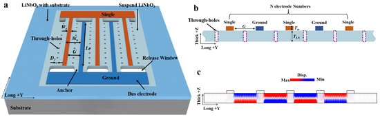
Figure 1.
A1 resonators based on LiNbO3 film (including through-holes structure). (a) Global schematic diagram of the resonator. (b) Cross-sectional view of the resonator. (c) Out-of-plane displacement field distribution in the resonator at its resonant frequency.
In order to obtain a suspended structure, it is generally necessary to etch through the LiNbO3 thin film to form release windows at the regions between the IDT electrodes and the Bus electrodes. Afterward, silicon (Si) or silicon oxide (SiO2) at the bottom of the LiNbO3 thin film is removed by wet or dry etching.
In the A1 resonators, acoustic energy is mainly concentrated in the transverse center of the resonators, with relatively minimal energy in the regions on either side. Typically, this phenomenon becomes more pronounced as the number of IDT electrodes increases [31,42]. Our study also verified this phenomenon. Figure 1c shows the distribution of the displacement field in the out-of-plane direction at the A1 resonating frequency. It can be seen that almost all vibrations of the A1 mode are in the region between the IDT electrodes, with virtually no vibration in the regions on either side. This is another advantage of the A1 resonators (also applicable to other thickness modes, e.g., A3). During the fabrication of the resonators, unlike non-thickness modes (e.g., S0 and SH0) resonators [44,45,46], the A1 resonators are less demanding on the broadening, sidewall inclination and roughness of the suspended LiNbO3 thin film boundary, offering considerable process convenience.
As mentioned earlier, the higher-order spurious modes in A1 resonators have a crucial relationship with the electrode design. In the previous designs, it is especially closely related to the electrode duty ratio. The duty ratio depends on the electrode width (We) and the electrode pitch (G), and a small ratio (generally < 0.15) is needed for the suppression of spurious modes. In previous approaches, reducing We and/or increasing G are mainly used to obtain a small duty ratio. However, overly large G (e.g., over 10 μm) will increase the device area, especially for resonators with a large number of electrodes. Also, the substrate/box-layer etching (release) time increases significantly, making the resonators more difficult to process. In addition, an excessively large suspension area of the LiNbO3 thin film will impair the stability and miniaturization of the resonators. On the other hand, with small We (e.g., less than 1 μm), although the spurious modes can be suppressed by moderate G, the requirements for lithographic precision are significantly increased. Therefore, it is challenging to achieve spurious mode-free A1 resonators with the smaller G and larger We.
Aiming at this problem, we propose a method to realize ideal LiNbO3 A1 resonators. By introducing subwavelength through-holes between IDT electrodes with large widths and small pitches, the spurious modes of resonators can be suppressed perfectly. As an example, our A1 resonators are prepared on a 300 nm LiNbO3 thin film, where the IDTs are modes of Gold (Au) with a thickness of 50 nm. Key parameters of our A1 resonators are marked in the model schematic (Figure 1a). Uniformly sized through-holes are periodically distributed across the suspended LiNbO3 thin film; their diameter is D1. The IDT electrode is perpendicular to the Y direction of LiNbO3; the electrode width is We, the electrode aperture is Le, the electrode pitch is G, the electrode duty ratio is C (its value is equal to We/(We + G)), and the number of electrodes is N. The specific values of these key parameters are given in Table 1.

Table 1.
Geometric parameter range of the A1 resonators studied in this paper.
In a 2D Lamb wave resonator model (as Figure 1b), the resonant frequency can be given by Equation (1), where m and n are the mode orders in the vertical (z-axis) and longitudinal (y-axis) directions, respectively. Vt is the acoustic velocity in the direction of the LiNbO3 thin film thickness, VL is the acoustic velocity in the direction perpendicular to the IDT electrode within the thin film plane, t is the LiNbO3 thin film thickness, and Wu is equal to the sum of the electrode pitch (G) and width (We). Both Vt and VL are closely related to the piezoelectricity of the LiNbO3. For the A1 mode resonators discussed in this paper, that is, m = 1, n = 1.
3. Suppression of Spurious Modes by Through-Holes Structure
To validate the spurious modes-suppression by the through-holes, we calculated the admittance spectra of the A1 resonators with and without the through-holes by 3D multi-physics simulation, as shown in Figure 2. In these A1 resonators, We = 2 μm, G = 8 μm, and Le = 90 μm. Figure 2a–f show the admittance spectra for the through-holes diameter (D1) at 0 μm (i.e., no through-holes), 0.25 μm, 0.50 μm, 0.75 μm, 1.00 μm, and 1.25 μm, respectively.
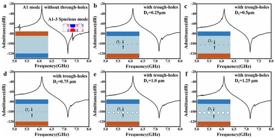
Figure 2.
Through-holes diameter on spurious mode suppression. (a−f) The diameters of through-holes are 0 μm (i.e., no through-holes), 0.25 μm, 0.50 μm, 0.75 μm, 1.00 μm, and 1.25 μm, respectively.
In the absence of the through-holes (Figure 2a), the A1 resonator has explicit spurious modes in its admittance spectrum. Analysis of the field distribution of an obvious spurious mode (see inset) shows that the spurious mode presents a lateral third-order form of the A1 mode. Generally, it is called the lateral third-order A1 mode (i.e., m = 1, n = 3) or A1–3 mode, which may be produced by acoustic reflection at the edges of the IDT electrodes [43]. When the through-holes are relatively small, e.g., D1 = 0.25 μm (Figure 2b), the spurious mode is suppressed to a great extent but still presents. As the through-holes become larger, e.g., D1 = 0.50 μm (Figure 2c), the spurious mode is completely suppressed. When their diameter is continuously increased, e.g., D1 = 0.75 μm (Figure 2d) and D1 = 1.00 μm (Figure 2e), the spurious mode is all in suppression. With the further enlargement of the through-holes, e.g., D1 = 1.25 μm (Figure 2f), the spurious mode reappears but is still faint. In all the above cases, the A1 resonators’ admittance and the frequencies of the primary mode remain almost the same.
We further studied the spurious modes-suppression on the different spacing of the through-holes, as shown in Figure 3. Take the resonator in Figure 2e; for instance, Figure 3a–f show admittance spectra that the spacing between two adjacent through-holes is 7 μm, 8 μm, 9 μm, 10 μm, 11 μm, and 12 μm, respectively. It can be seen that when the spacing is small, e.g., 7 μm (Figure 3a), the spurious modes are already suppressed quite well, but there is still a little bit. They are completely suppressed with increased spacing, e.g., 8 μm to 10 μm (Figure 3b–d). When the spacing continues to increase, e.g., 11 μm and 12 μm (Figure 3e,f), the spurious mode reappears, but still only a little bit, much better than the situation without through-holes. Also, in these above cases, the A1 resonators’ admittance and the frequencies of the primary mode remain almost the same.
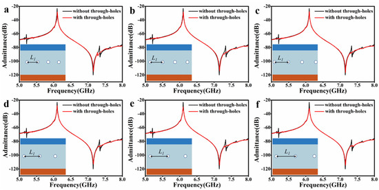
Figure 3.
Through-holes’ spacings on spurious modes-suppression. (a–f) The spacings between two adjacent through-holes are 7 μm, 8 μm, 9 μm, 10 μm, 11 μm, and 12 μm, respectively.
We also studied the influence of the position of the through-holes between the IDT electrodes on the spurious modes-suppression, as shown in Figure 4. Take the same resonator in Figure 2e as an instance, Figure 4a–f show the admittance spectra for the position of the through-holes moved upward by 0.5 μm, 1 μm, 1.5 μm and downward by 0.5 μm, 1 μm, and 1.5 μm, respectively. The results show that as long as the position of the through-holes is among the IDT electrodes, all unwanted spurious modes are completely suppressed.
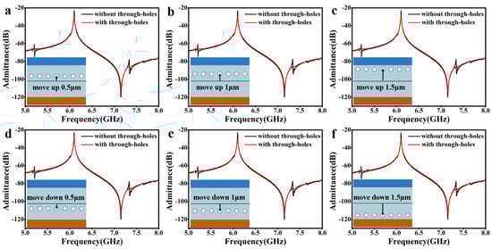
Figure 4.
Through-holes position on spurious modes-suppression. (a–c) All the through-holes are moved upward 0.5 μm, 1 μm, and 1.5 μm, respectively. (d–f) All the through-holes are moved downward 0.5 μm, 1 μm, and 1.5 μm, respectively.
In summary, for different hole sizes, spacings, and positions, the through-holes have a wide design window for the spurious modes-suppression of the A1 resonators. Also, compared with the LiNbO3 thickness (i.e., 300 nm in this study), the geometric depth-to-width ratio of the through-holes is quite small, making them convenient to fabricate.
4. Wide Applicability of the Through-Holes for IDT Designs
To implement well-functioning A1 filters, the IDT electrodes of the A1 resonators typically need to have various apertures and electrode duty ratios. Our through-holes for spurious mode-free resonators are well-applicable to different IDT designs. To demonstrate this, we calculated the admittance spectra of A1 resonators with identical through-holes for various IDT designs, as shown in Figure 5. Figure 5a–c show the admittance spectra for different electrode duty ratio (C). Figure 5d–f show the spectra for different IDT apertures. Specific values of the resonators’ parameters are labeled in the figures.
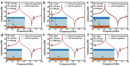
Figure 5.
Spurious modes-suppression by the through-holes (D1 = 1 μm) with different IDT designs. (a–c): Wu = 10 μm, Le = 90 μm, We = 1.5 μm, 2.0 μm, and 2.5 μm, respectively. (d–f): Wu = 10 μm, We = 2.0 μm, Le = 80 μm, 100 μm, and 110 μm, respectively.
Without the through-holes, a spurious mode (A1–3 mode) at a higher frequency near the anti-resonant peak is present in all the resonators. In some resonators, another distinct spurious mode appears at a lower frequency near the main resonant peak. When the through-holes (D1 = 1.0 μm) are introduced, both spurious modes near the anti-resonance and main resonance peaks are well suppressed.
5. Wide Applicability of the Through-Holes for LiNbO3 Thickness
As mentioned in the introduction part, another advantage of the A1 resonators is that their operating frequencies are largely dependent on the thickness of the LiNbO3 thin film. By thinning the LiNbO3 thin film regionally, a single LiNbO3 thin film can have different thicknesses in different regions, thereby supporting A1 resonators with two or even multiple resonating frequencies. For variable thicknesses of the LiNbO3 thin films, the through-holes also have great applicability. Two randomly selected A1 resonators incorporating the through-holes were used as examples, and their admittance spectra were calculated for the variations of LiNbO3 thickness. The results are shown in Figure 6. Specific parameters of the resonators are marked in the figure. As can be seen, when thinning the LiNbO3 from 300 nm to 250 nm, no spurious mode appears in both two A1 resonators. At the same time, their resonant frequencies increase linearly.
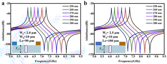
Figure 6.
A1 resonators containing through-holes during thinning of the LiNbO3 thin film from 300 nm to 250 nm. IDT parameters of the two resonators are (a) Wu = 10 μm, We = 2 μm, Le = 90 μm and (b) Wu = 10 μm, We = 2.5 μm, Le = 100 μm.
6. Advantages of the Through-Holes for Device Fabrication and Stability
The through-holes also have important advantages for the processing and stability of the resonators (and subsequent filters), mainly involving two aspects.
Firstly, the preparation convenience of the through-holes itself, i.e., the introduction of the through-holes, does not add additional process steps. To prepare such Lamb wave resonators, it is usually necessary to etch several release windows on the piezoelectric (e.g., LiNbO3) thin film [31,42]. All through-holes can be fabricated simultaneously.
Secondly, and more importantly, the last step in the preparation of such resonators is to release the LiNbO3 thin film, i.e., to etch the box layer (e.g., SiO2) or substrate (Si) at the bottom of the piezoelectric thin film. The through-holes can significantly reduce the release process time and greatly reduce the invalid suspension area of the LiNbO3 thin film. Figure 7 shows the geometries of two resonators after the release (etching) process with and without the through-holes. Without through-holes, corrosive liquid or gas used to etch the SiO2/Si can only enter from peripheral release windows. Since the etching process is isotropic, while the LiNbO3 thin film with IDT is completely suspended, it also leads to a large invalid LiNbO3 suspension area around the resonator. This is detrimental to the mechanical and temperature stability of all Lamb wave resonators. When the through-holes are introduced, in addition to the original release windows, all the through-holes also act as release windows to enter corrosive liquids or gases. In this way, the LiNbO3 thin film with IDT can be suspended completely by enduring only a small amount of etching, which significantly reduces the area of the invalid LiNbO3 suspension area around the resonator, and greatly improves the stability of the resonator (and subsequent filters).
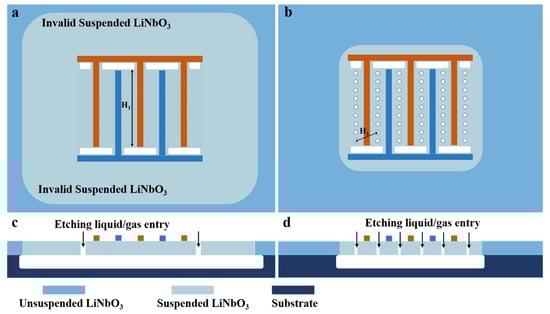
Figure 7.
Geometries of the resonators after the release (etching) process without (a) top view (c) (cross-section view) and with (b) top view (d) (cross-section view) of the through-holes. H1 indicates the maximum etching/corrosion spacing.
7. Conclusions
In this paper, we propose a general method for ideal LiNbO3 A1 resonators. By introducing subwavelength through-holes (with broad size requirement) among the IDT electrodes on the surface of the LiNbO3, all unwanted spurious modes can be completely suppressed. It is well-applicable under different IDT designs and LiNbO3 thicknesses.
For the fabrication of the A1 resonators and filters, no additional steps are required for the through-holes. Meanwhile, due to the existence of the through-holes, the etch (release) time for the substrate/box-layer (Si or SiO2) is drastically reduced. While improving the design flexibility, the invalid suspension area of the LiNbO3 thin film is also reduced, thus improving the compactness, mechanical stability, temperature stability, and power tolerance of the A1 resonators/filters. Our paper takes Z-cut LiNbO3 A1 resonators as an example. For other crystallographic orientations (e.g., 128° Y-cut), this design is also applicable. Also, for other Lamb waves resonators using different modes (e.g., other A, S, or SH modes) or different materials (e.g., AlN or AlScN), the through-holes may also have similar advantages, at least in terms of design convenience, processing convenience, and stability. Due to these advantages, we believe it will serve as a general solution and facilitate the practical application of Lamb wave resonators and filters.
Author Contributions
Conceptualization, S.-M.W. and S.-Y.Y.; methodology, S.-M.W., C.-B.H. and Z.-H.Q.; software, S.-M.W., C.-B.H. and Z.-H.Q.; validation, S.-M.W. and S.-Y.Y.; formal analysis, S.-M.W.; investigation, S.-M.W., S.-Y.Y., C.-B.H. and Y.W.; resources, S.-Y.Y. and Y.-F.C.; data curation, S.-M.W. and C.-B.H.; writing—original draft preparation, S.-M.W., H.-Y.C. and S.-Y.Y.; writing—review and editing, S.-M.W. and S.-Y.Y.; project administration, S.-Y.Y. and Y.-F.C. All authors have read and agreed to the published version of the manuscript.
Funding
The work was jointly supported by the National Key R & D Program of China (Grant Nos. 2021YFB3801801 and 2022YFA1404404) and the National Natural Science Foundation of China (Grant Nos. 11890702, 92163133, and 12172164). We also acknowledge the support of the Fundamental Research Funds for Central Universities (China).
Data Availability Statement
Not applicable.
Conflicts of Interest
The authors declare no conflict of interest.
References
- Jyomura, S.; Nagatsuma, K.; Takeuchi, H. SAW propagation loss mechanism in piezoelectric ceramics. J. Appl. Phys. 1981, 52, 4472–4478. [Google Scholar] [CrossRef]
- Hagelauer, A.; Fattinger, G.; Ruppel, C.C.W.; Ueda, M.; Hashimoto, K.-Y.; Tag, A. Microwave Acoustic Wave Devices: Recent Advances on Architectures, Modeling, Materials, and Packaging. IEEE Trans. Microw. Theory Tech. 2018, 66, 4548–4562. [Google Scholar] [CrossRef]
- Gong, S.; Lu, R.; Yang, Y.; Gao, L.; Hassanien, A.E. Microwave Acoustic Devices: Recent Advances and Outlook. IEEE J. Microw. 2021, 1, 601–609. [Google Scholar] [CrossRef]
- Kim, D.; Moreno, G.; Bi, F.; Winters, M.; Houlden, R.; Aichele, D.; Shealy, J. Wideband 6 GHz RF Filters for Wi-Fi 6E Using a Unique BAW Process and Highly Sc-doped AlN Thin Film. In Proceedings of the 2021 IEEE MTT-S International Microwave Symposium (IMS), Atlanta, GA, USA, 7–25 June 2021; pp. 207–209. [Google Scholar]
- Lee, J.; Tejedor, E.; Ranta-Aho, K.; Wang, H.; Lee, K.-T.; Semaan, E.; Mohyeldin, E.; Song, J.; Bergljung, C.; Jung, S. Spectrum for 5G: Global Status, Challenges, and Enabling Technologies. IEEE Commun. Mag. 2018, 56, 12–18. [Google Scholar] [CrossRef]
- Yandrapalli, S.; Liffredo, M.; Faizan, M.; Küçük, S.; Maillard, D.; Villanueva, L.G. Thin Film Devices for 5G Communications. In Proceedings of the 2021 IEEE 34th International Conference on Micro Electro Mechanical Systems (MEMS), Gainesville, FL, USA, 25–29 January 2021; pp. 450–453. [Google Scholar]
- Aigner, R. Filter technologies for converged RF-frontend architectures: SAW, BAW and beyond. In Proceedings of the 10th Topical Meeting on Silicon Monolithic Integrated Circuits in RF Systems (SiRF2010), New Orleans, LA, USA, 11–13 January 2010. [Google Scholar]
- Shen, J.; Fu, S.; Su, R.; Xu, H.; Lu, Z.; Zhang, Q.; Zeng, F.; Song, C.; Wang, W.; Feng, P. SAW Filters With Excellent Temperature Stability and High Power Handling Using LiTaO3/SiC Bonded Wafers. J. Microelectromech. Syst. 2022, 31, 186–193. [Google Scholar] [CrossRef]
- Akai, T.; Iwamoto, H.; Takamine, Y.; Yamazaki, H.; Fuyutsume, T.; Kyoya, H.; Nakao, T.; Kando, H.; Hiramoto, M.; Toi, T.; et al. High-Performance SAW Resonator on New Multilayered Substrate Using LiTaO3 Crystal. IEEE Trans. Ultrason. Ferroelectr. Freq. Control 2017, 64, 1382–1389. [Google Scholar]
- Takai, T.; Iwamoto, H.; Takamine, Y.; Fuyutsume, T.; Nakao, T.; Hiramoto, M.; Toi, T.; Koshino, M. IHPSAW Technology and its Application to Microacoustic Components (Invited). In Proceedings of the IEEE International Ultrasonics Symposium (IUS), Washington, DC, USA, 6–9 September 2017. [Google Scholar]
- Shen, J.; Fu, S.; Su, R.; Xu, H.; Lu, Z.; Xu, Z.; Luo, J.; Zeng, F.; Song, C.; Wang, W.; et al. High-Performance Surface Acoustic Wave Devices Using LiNbO3/SiO2/SiC Multilayered Substrates. IEEE Trans. Microw. Theory Technol. 2021, 69, 3693–3705. [Google Scholar] [CrossRef]
- Wu, J.; Zhang, S.; Chen, Y.; Zheng, P.; Zhang, L.; Yao, H.; Li, Z.; Zhao, X.; Huang, K.; Wu, T.; et al. Advanced Surface Acoustic Wave Resonators on LiTaO₃/SiO₂/Sapphire Substrate. IEEE Electron Device Lett. 2022, 43, 1748–1751. [Google Scholar] [CrossRef]
- Wu, J.; Zhang, S.; Zhang, L.; Zhou, H.; Zheng, P.; Yao, H.; Li, Z.; Huang, K.; Wu, T.; Ou, X. Exploring Low-Loss Surface Acoustic Wave Devices on Heterogeneous Substrates. IEEE Trans. Ultrason. Ferroelectr. Freq. Control 2022, 69, 2579–2584. [Google Scholar] [CrossRef]
- Su, R.; Fu, S.; Shen, J.; Lu, Z.; Xu, H.; Wang, R.; Song, C.; Zeng, F.; Wang, W.; Pan, F. Wideband Surface Acoustic Wave Filter at 3.7 GHz With Spurious Mode Mitigation. IEEE Trans. Microw. Theory Tech. 2023, 71, 480–487. [Google Scholar] [CrossRef]
- Kimura, T.; Omura, M.; Kishimoto, Y.; Hashimoto, K. Comparative Study of Acoustic Wave Devices Using Thin Piezoelectric Plates in the 3-5-GHz Range. IEEE Trans. Microw. Theory Tech. 2019, 67, 915–921. [Google Scholar] [CrossRef]
- Ding, R.; Xuan, W.; Dong, S.; Zhang, B.; Gao, F.; Liu, G.; Zhang, Z.; Jin, H.; Luo, J. The 3.4 GHz BAW RF Filter Based on Single Crystal AlN Resonator for 5G Application. Nanomaterials 2022, 12, 3082. [Google Scholar] [CrossRef]
- Shealy, J.B.; Vetury, R.; Gibb, S.R.; Hodge, M.D.; Patel, P.; McLain, M.A.; Feldman, A.Y.; Boomgarden, M.D.; Lewis, M.P.; Hosse, B.; et al. Low Loss, 3.7GHz Wideband BAW Filters, Using High Power Single Crystal AlN-on-SiC Resonators. In Proceedings of the IEEE-Microwave-Theory-and-Techniques-Society International Microwave Symposium (IMS)/Session on Women in Microwaves (WIM), Honolulu, HI, USA, 4–9 June 2017. [Google Scholar]
- Zhao, W.; Asadi, M.J.; Li, L.; Chaudhuri, R.; Nomoto, K.; Xing, H.G.; Hwang, J.C.M.; Jena, D. X-band epi-BAW resonators. J. Appl. Phys. 2022, 132, 024503. [Google Scholar] [CrossRef]
- Zou, Y.; Gao, C.; Zhou, J.; Liu, Y.; Xu, Q.; Qu, Y.; Liu, W.; Woon Soon, J.B.; Cai, Y.; Sun, C. Aluminum scandium nitride thin-film bulk acoustic resonators for 5G wideband applications. Microsyst. Nanoeng. 2022, 8, 124. [Google Scholar] [CrossRef]
- Trolier-McKinstry, S.; Muralt, P. Thin Film Piezoelectrics for MEMS. J. Electroceram. 2004, 12, 7–17. [Google Scholar] [CrossRef]
- Liu, Y.; Cai, Y.; Zhang, Y.; Tovstopyat, A.; Liu, S.; Sun, C. Materials, Design, and Characteristics of Bulk Acoustic Wave Resonator: A Review. Micromachines 2020, 11, 630. [Google Scholar] [CrossRef]
- Vetury, R.; Hodge, M.D.; Shealy, J.B. High Power, Wideband Single Crystal XBAW Technology for sub-6 GHz Micro RF Filter Applications. In Proceedings of the IEEE International Ultrasonics Symposium (IUS), Kobe, Japan, 22–25 October 2018. [Google Scholar]
- Zou, Y.; Cai, Y.; Gao, C.; Luo, T.; Liu, Y.; Xu, Q.; Wang, Y.; Nian, L.; Liu, W.; Soon, J.B.W.; et al. Design, Fabrication, and Characterization of Aluminum Scandium Nitride-Based Thin Film Bulk Acoustic Wave Filter. J. Microelectromech. Syst. 2023, 32, 263–270. [Google Scholar] [CrossRef]
- AlJoumayly, M.; Rothemund, R.; Schaefer, M.; Heeren, W. 5G BAW Technology: Challenges and Solutions. In Proceedings of the 2022 IEEE 22nd Annual Wireless and Microwave Technology Conference (WAMICON), Clearwater, FL, USA, 27–28 April 2022; pp. 1–3. [Google Scholar]
- Kadota, M.; Ogami, T.; Yamamoto, K.; Tochishita, H.; Negoro, Y. High-Frequency Lamb Wave Device Composed of MEMS Structure Using LiNbO3 Thin Film and Air Gap. IEEE Trans. Ultrason. Ferroelectr. Freq. Control 2010, 57, 2564–2571. [Google Scholar] [CrossRef]
- Lu, R.; Gong, S. RF acoustic microsystems based on suspended lithium niobate thin films: Advances and outlook. J. Micromech. Microeng. 2021, 31, 114001. [Google Scholar] [CrossRef]
- Yang, Y.; Lu, R.; Gong, S. A 1.65 GHz Lithium Niobate A1 Resonator with Electromechanical Coupling of 14% and Q of 3112. In Proceedings of the 32nd IEEE International Conference on Micro Electro Mechanical Systems (IEEE MEMS), Seoul, Republic of Korea, 27–31 January 2019. [Google Scholar]
- Yang, Y.; Gao, A.; Lu, R.; Gong, S. 5 GHz Lithium Niobate Mems Resonators with High FOM of 153. In Proceedings of the 30th IEEE International Conference on Micro Electro Mechanical Systems (MEMS), Las Vegas, NV, USA, 22–26 January 2017. [Google Scholar]
- Yang, Y.; Lu, R.; Manzaneque, T.; Gong, S. 1.7 GHz Y-Cut Lithium Niobate MEMS Resonators with FoM of 336 and f.Q of 9.15 × 10¹². In Proceedings of the IEEE-MTT-Society International Microwave Symposium (IMS), Philadelphia, PA, USA, 10–15 June 2018. [Google Scholar]
- Lu, R.; Yang, Y.; Gong, S. 5 GHz A1 Mode Lateral Overtone Bulk Acoustic Resonators in Thin-Film Lithium Niobate. In Proceedings of the IEEE International Ultrasonics Symposium (IEEE IUS), Las Vegas, NV, USA, 7–11 September 2020. [Google Scholar]
- Lu, R.; Yang, Y.; Link, S.; Gong, S. A1 Resonators in 128° Y-cut Lithium Niobate with Electromechanical Coupling of 46.4%. J. Microelectromech. Syst. 2020, 29, 313–319. [Google Scholar] [CrossRef]
- Plessky, V.; Küçük, S.; Yandrapalli, S.; Villanueva, L.G. A formula for the admittance of laterally excited bulk wave resonators (XBARs). Electron. Lett. 2021, 57, 773–775. [Google Scholar] [CrossRef]
- Plessky, V.; Yandrapalli, S.; Turner, P.; Villanueva, L.; Koskela, J.; Hammond, R. 5 GHz laterally-excited bulk-wave resonators (XBARs) based on thin platelets of lithium niobate. Electron. Lett. 2019, 55, 98–100. [Google Scholar] [CrossRef]
- Turner, P.J.; Garcia, B.; Yantchev, V.; Dyer, G.; Yandrapalli, S.; Villanueva, L.G.; Hammond, R.B.; Plessky, V. 5 GHz Band n79 wideband microacoustic filter using thin lithium niobate membrane. Electron. Lett. 2019, 55, 942–943. [Google Scholar] [CrossRef]
- Koulakis, J.; Koskela, J.; Yang, W.; Myers, L.; Dyer, G.; Garcia, B. XBAR physics and next generation filter design. In Proceedings of the 2021 IEEE International Ultrasonics Symposium (IUS), Xi’an, China, 11–16 September 2021; pp. 1–5. [Google Scholar]
- Plessky, V.; Yandrapalli, S.; Kucuk, S.; Villanueva, L.G. Resonance Frequency Dependence of A1 Lamb Mode On The Pitch Of The Electrode Structure. In Proceedings of the 2021 Joint Conference of the European Frequency and Time Forum and IEEE International Frequency Control Symposium (EFTF/IFCS), Gainesville, FL, USA, 7–17 July 2021; pp. 1–3. [Google Scholar]
- Wu, Z.; Yang, K.; Lin, F.; Zuo, C. 6.2 GHz Lithium Niobate MEMS Filter with FBW of 11.8% and IL of 1.7 dB. In Proceedings of the 2022 IEEE MTT-S International Conference on Microwave Acoustics and Mechanics (IC-MAM), Munich, Germany, 18–20 July 2022; pp. 98–101. [Google Scholar]
- Yang, Y.; Gao, L.; Gong, S. X-Band Miniature Filters Using Lithium Niobate Acoustic Resonators and Bandwidth Widening Technique. IEEE Trans. Microw. Theory Technol. 2021, 69, 1602–1610. [Google Scholar] [CrossRef]
- Su, R.; Yu, Z.; Fu, S.; Xu, H.; Zhang, S.; Liu, P.; Guo, Y.; Song, C.; Zeng, F.; Pan, F. Lithium Niobate Thin Film Based A1 Mode Resonators with Frequency up to 16 Ghz and Electromechanical Coupling Factor Near 35%. In Proceedings of the 2023 IEEE 36th International Conference on Micro Electro Mechanical Systems (MEMS), Munich, Germany, 15–19 January 2023; pp. 1190–1193. [Google Scholar]
- Yandrapalli, S.; Eroglu, S.E.K.; Plessky, V.; Atakan, H.B.; Villanueva, L.G. Study of Thin Film LiNbO3 Laterally Excited Bulk Acoustic Resonators. J. Microelectromech. Syst. 2022, 31, 217–225. [Google Scholar] [CrossRef]
- Yandrapalli, S.; Plessky, V.; Koskela, J.; Yantchev, V.; Turner, P.; Villanueva, L.G. Analysis of XBAR resonance and higher order spurious modes. In Proceedings of the IEEE International Ultrasonics Symposium (IUS), Glasgow, UK, 6–9 October 2019. [Google Scholar]
- Yang, Y.; Lu, R.; Gong, S. High Q Antisymmetric Mode Lithium Niobate MEMS Resonators with Spurious Mitigation. J. Microelectromech. Syst. 2020, 29, 135–143. [Google Scholar] [CrossRef]
- Yang, Y.; Gao, L.; Lu, R.; Gong, S. Lateral Spurious Mode Suppression in Lithium Niobate A1 Resonators. IEEE Trans. Ultrason. Ferroelectr. Freq. Control 2021, 68, 1930–1937. [Google Scholar] [CrossRef]
- Gong, S.; Piazza, G. Design and Analysis of Lithium–Niobate-Based High Electromechanical Coupling RF-MEMS Resonators for Wideband Filtering. IEEE Trans. Microw. Theory Technol. 2013, 61, 403–414. [Google Scholar] [CrossRef]
- Pop, F.V.; Kochhar, A.S.; Vidal-Alvarez, G.; Piazza, G. Investigation of Electromechanical Coupling and Quality Factor of X-Cut Lithium Niobate Laterally Vibrating Resonators Operating Around 400 MHz. J. Microelectromech. Syst. 2018, 27, 407–413. [Google Scholar] [CrossRef]
- Song, Y.-H.; Gong, S. Wideband RF Filters Using Medium-Scale Integration of Lithium Niobate Laterally Vibrating Resonators. IEEE Electron Device Lett. 2017, 38, 387–390. [Google Scholar] [CrossRef]
Disclaimer/Publisher’s Note: The statements, opinions and data contained in all publications are solely those of the individual author(s) and contributor(s) and not of MDPI and/or the editor(s). MDPI and/or the editor(s) disclaim responsibility for any injury to people or property resulting from any ideas, methods, instructions or products referred to in the content. |
© 2023 by the authors. Licensee MDPI, Basel, Switzerland. This article is an open access article distributed under the terms and conditions of the Creative Commons Attribution (CC BY) license (https://creativecommons.org/licenses/by/4.0/).