


Design and Optimization of Planar Spiral Coils for Powering Implantable Neural Recording Microsystem


Abstract
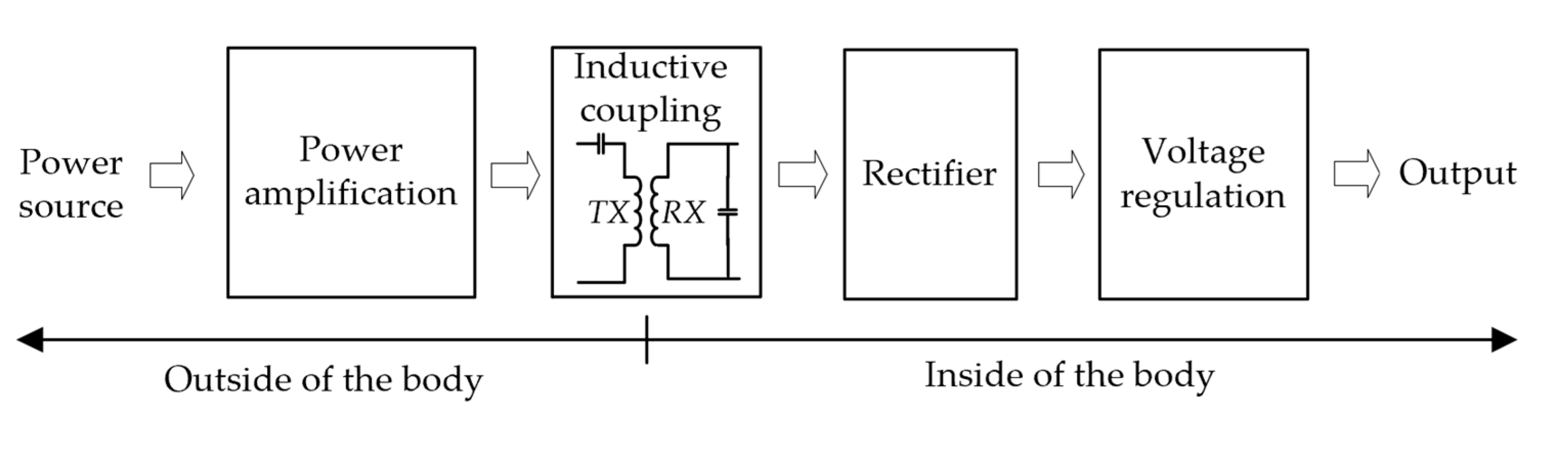
1. Introduction
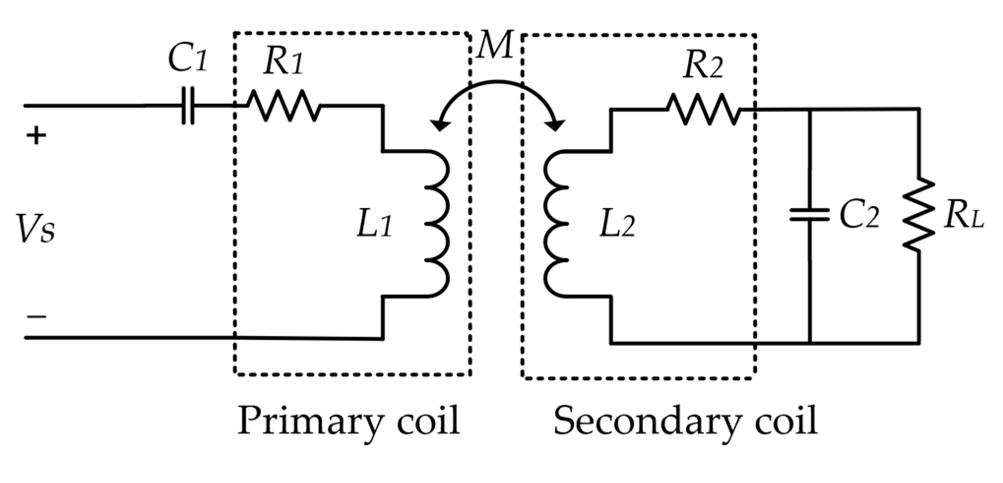
2. Modeling of Inductive Coupling
2.1. Maximum Power Transfer Efficiency and Optimal Load Condition
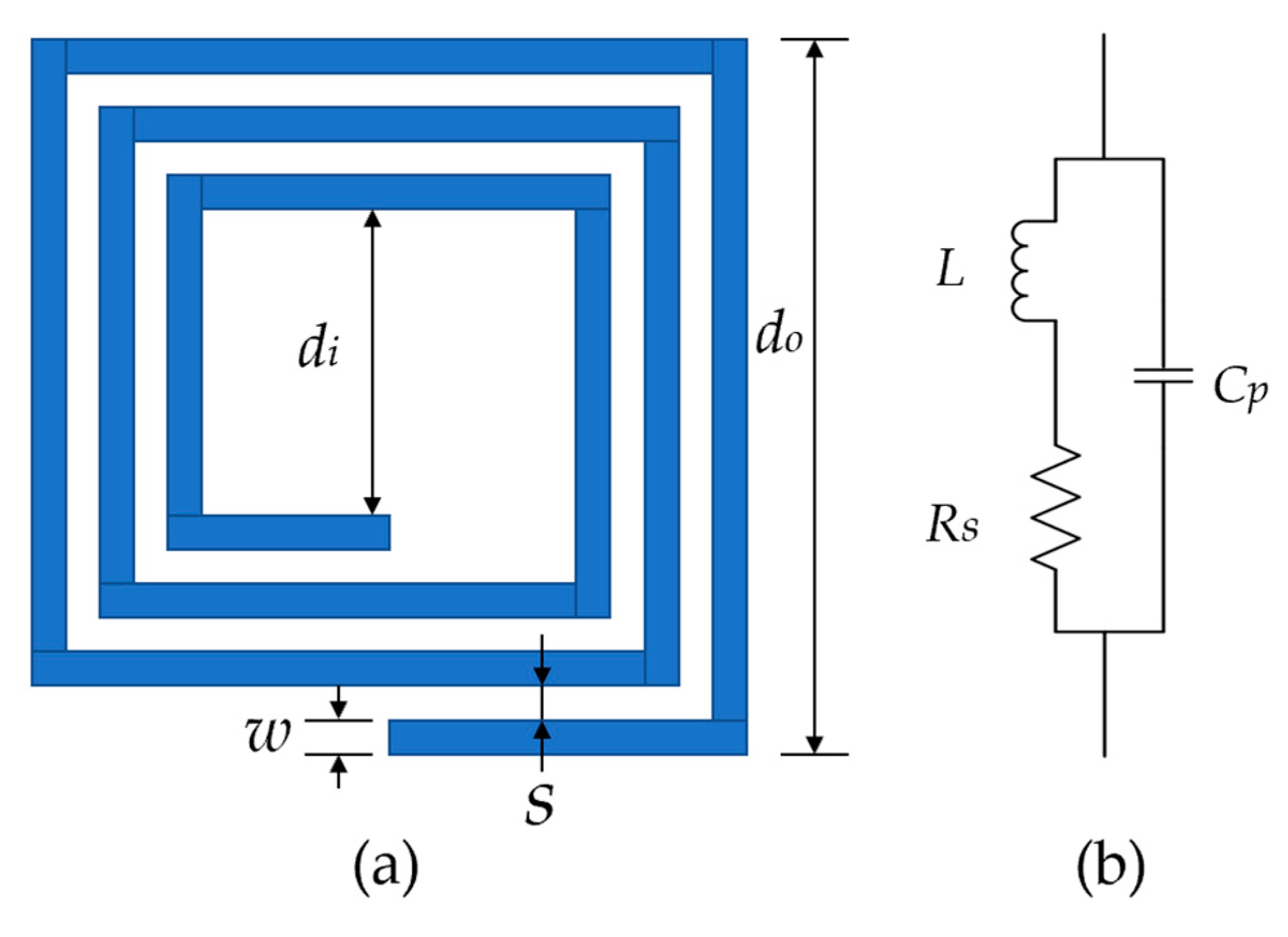
2.2. Planar Spiral Coil Modeling
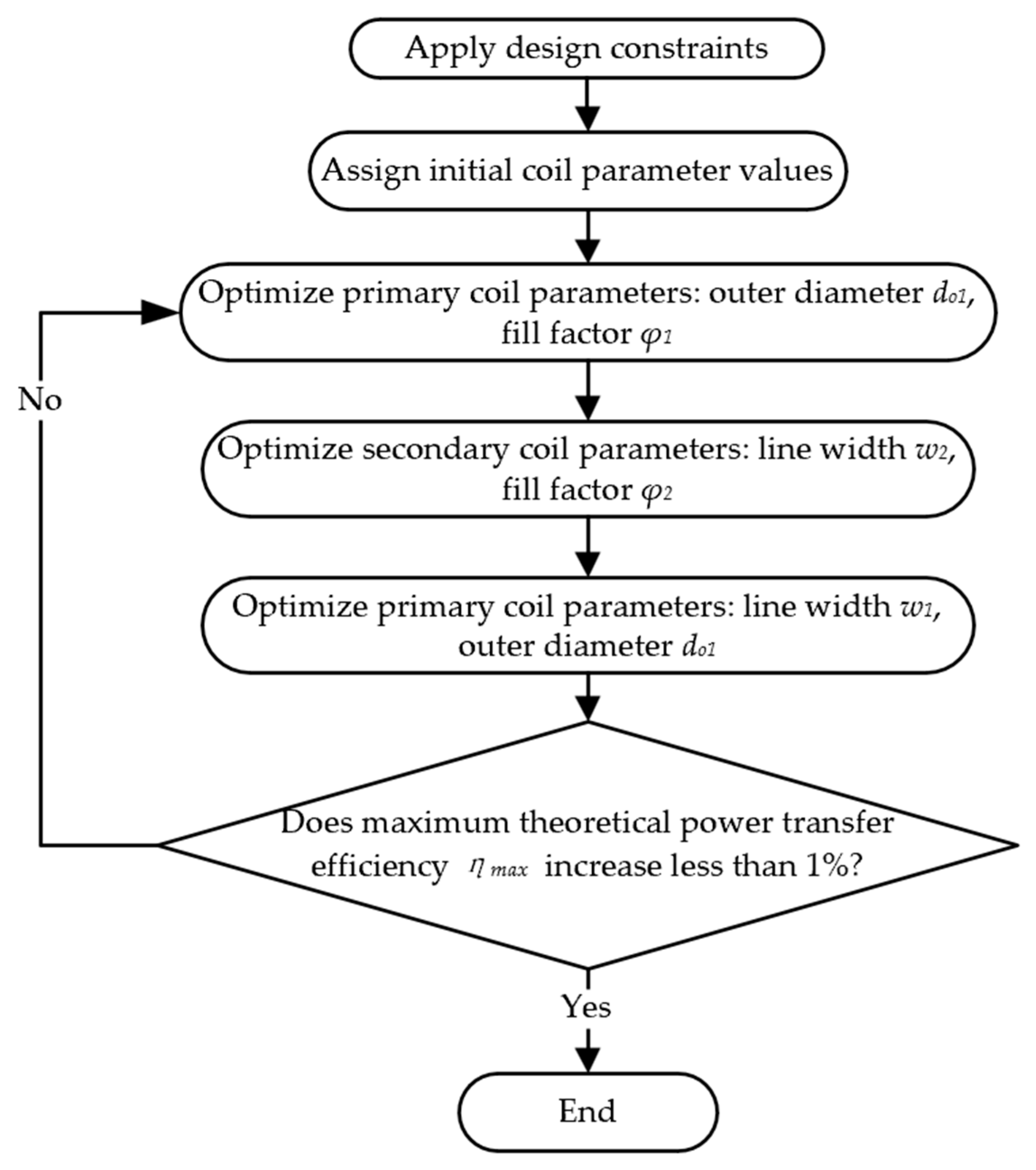
3. Design and Optimization of Planar Spiral Coils
3.1. Design Constraints
3.2. Optimization Process
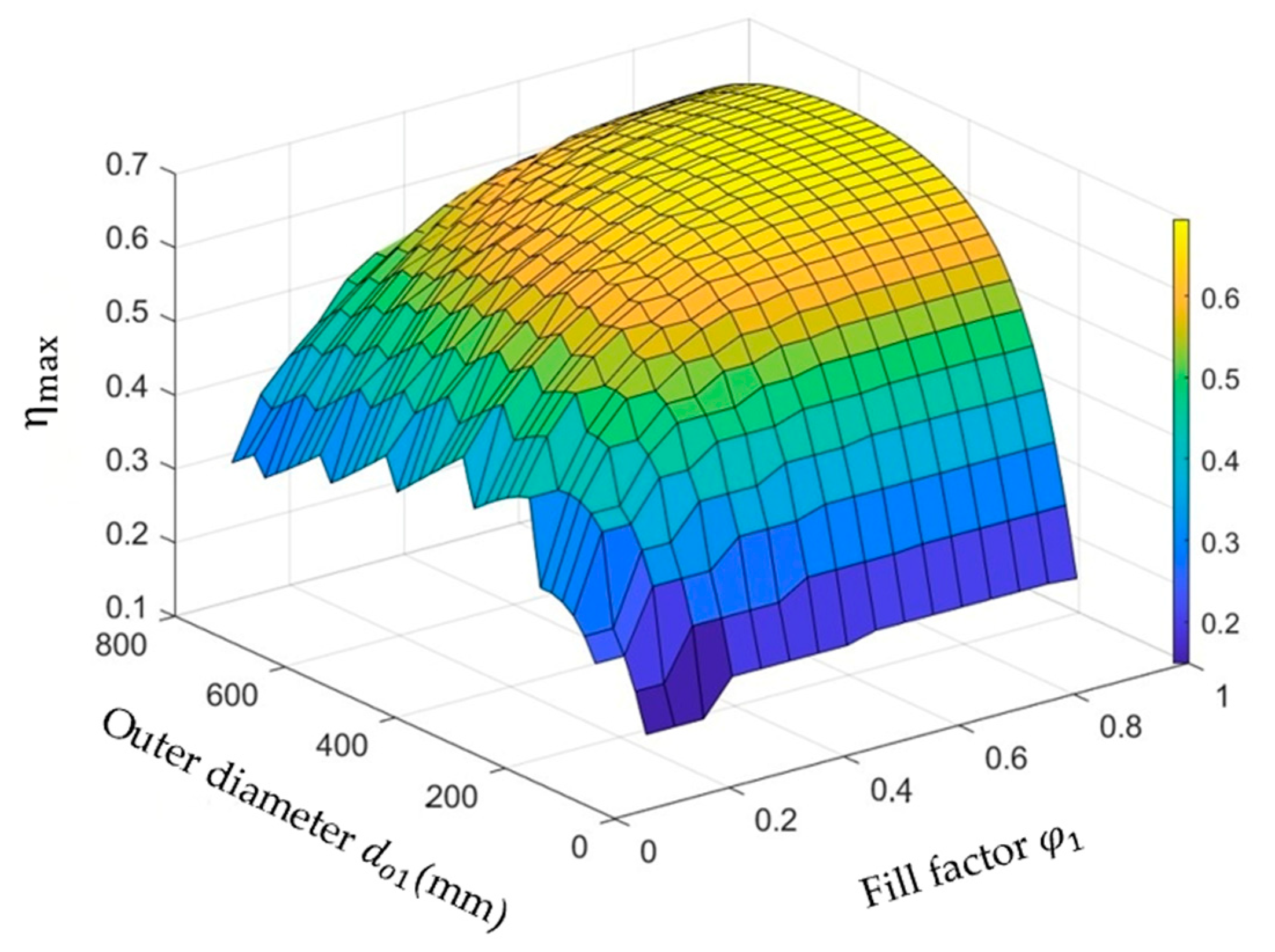
3.2.1. Optimize the Outer Diameter and Fill Factor of the Primary Coil
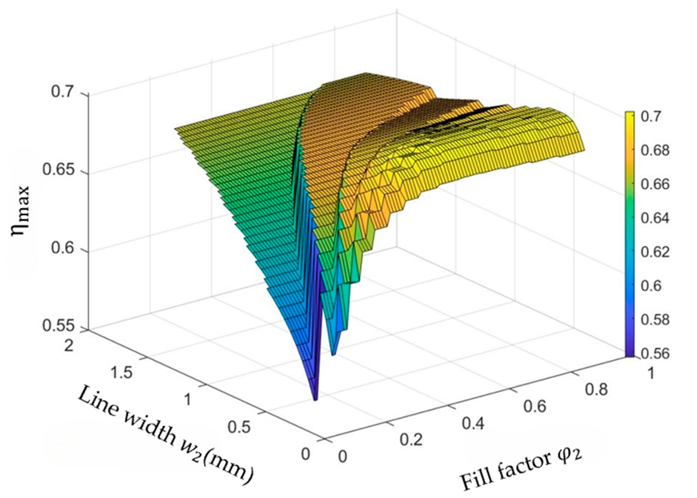
3.2.2. Optimize the Line Width and Fill Factor of the Secondary Coil
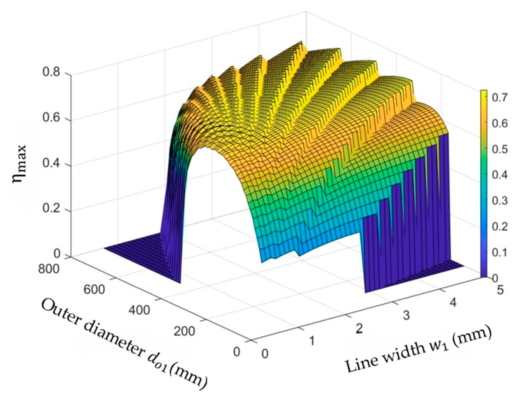
3.2.3. Optimize the Outer Diameter and Line Width of the Primary Coil
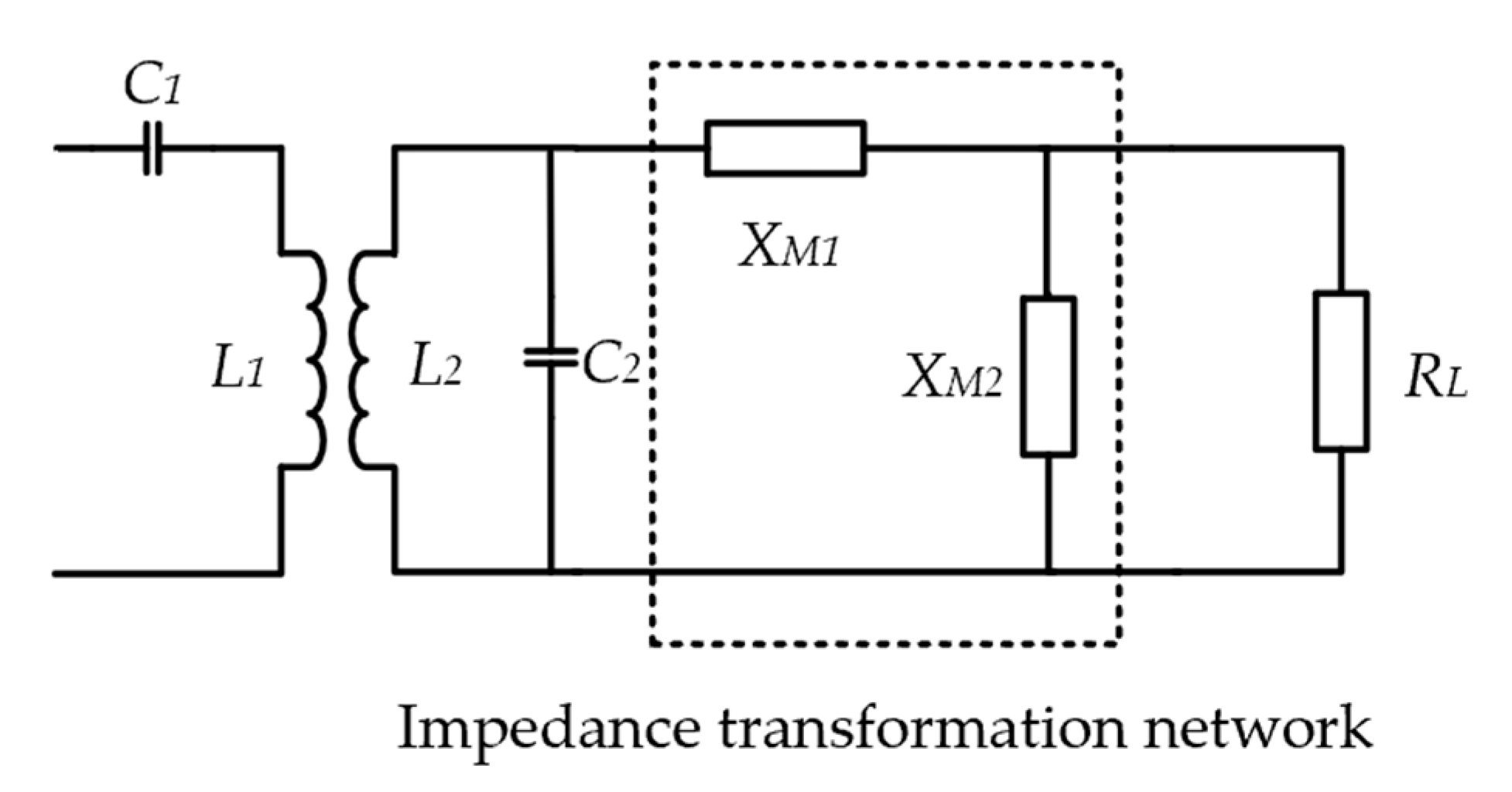
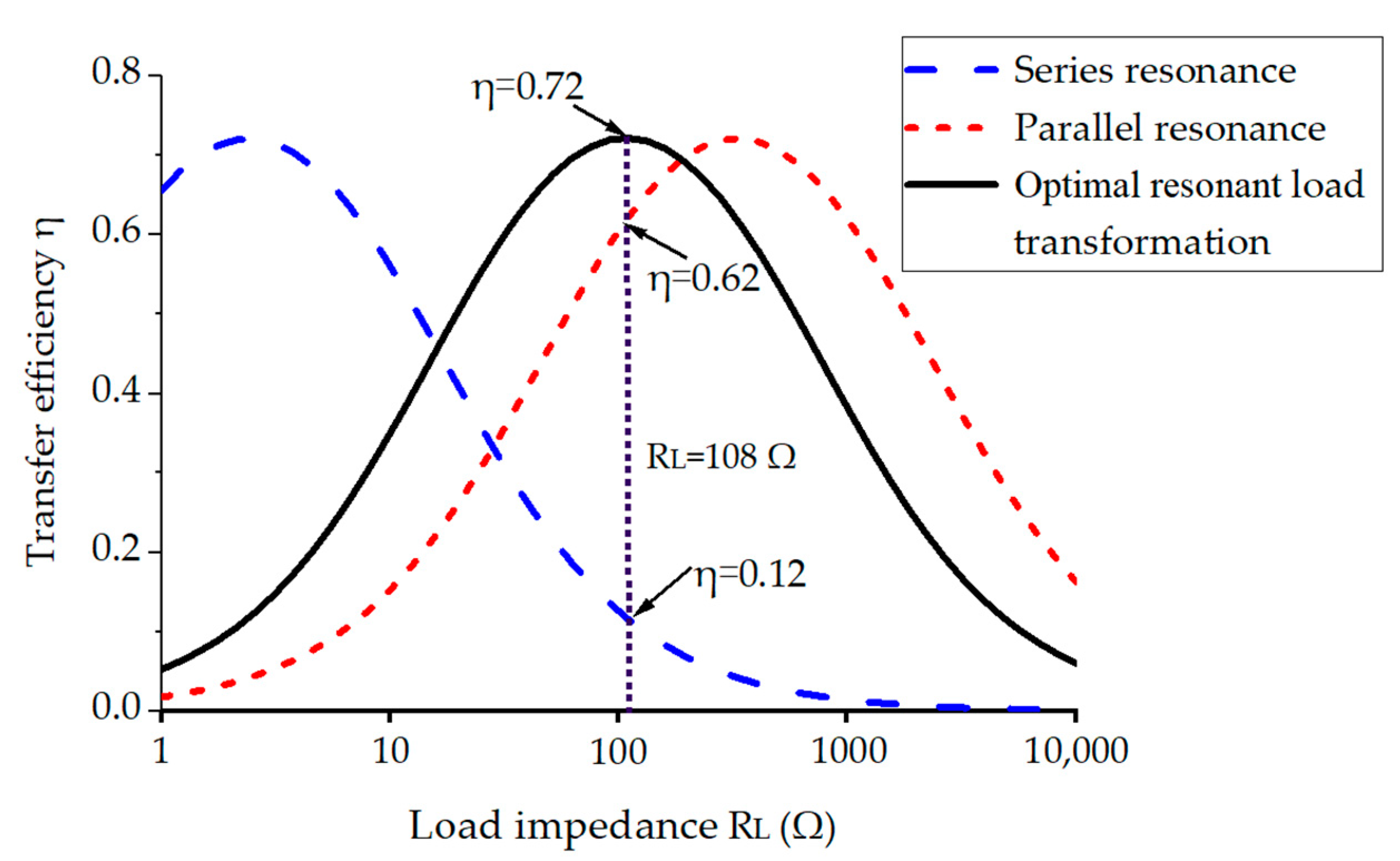
4. Optimal Resonant Load Transformation
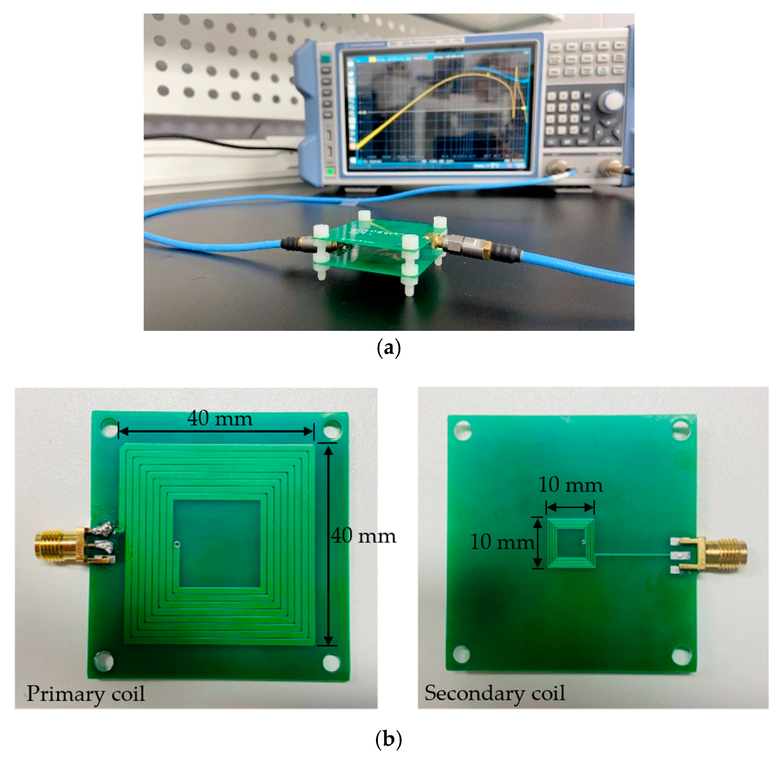
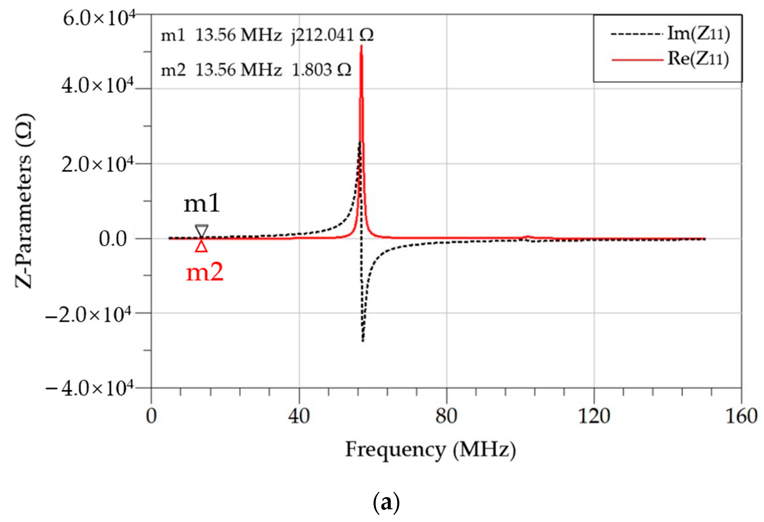
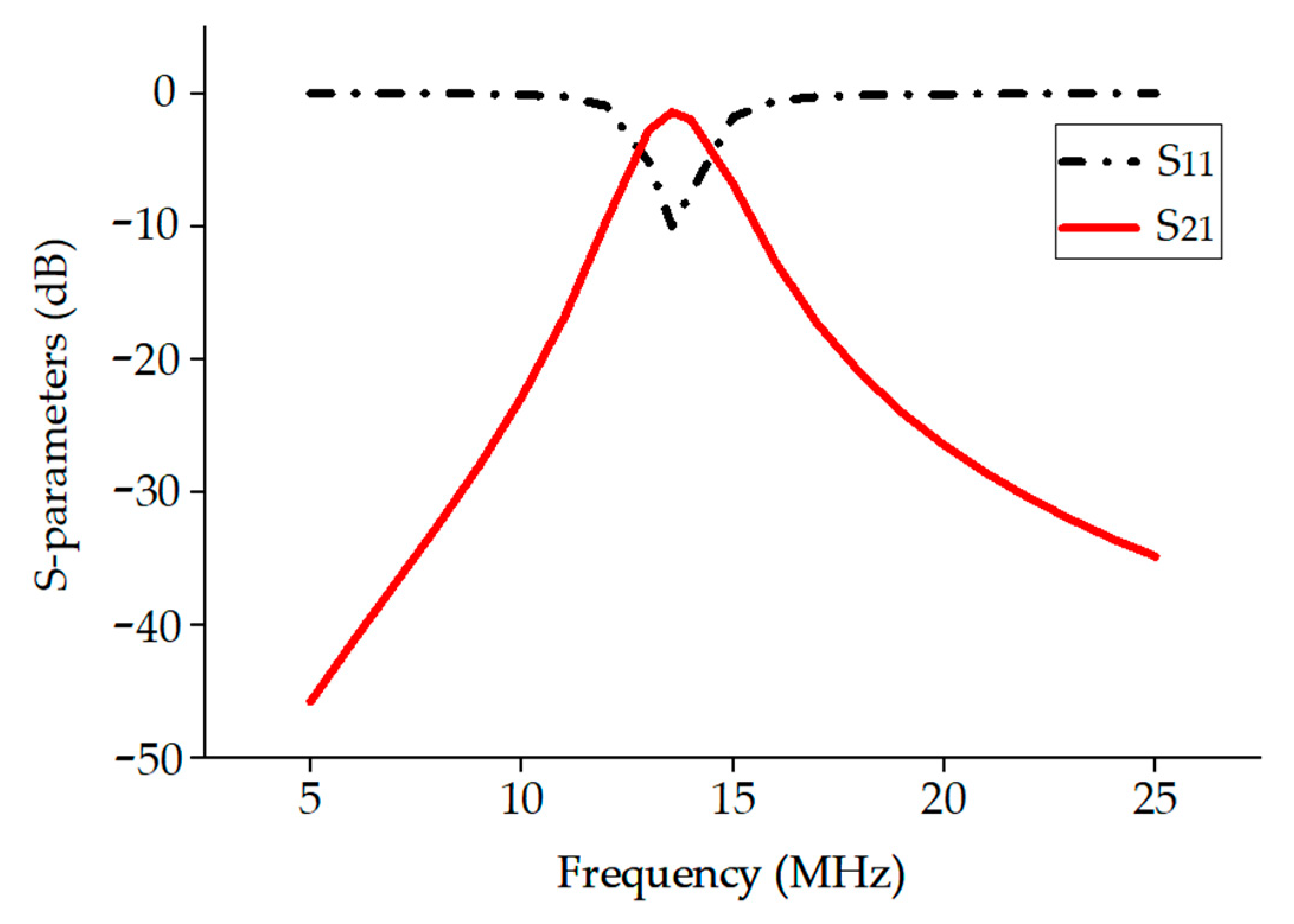
5. Electromagnetic Simulation and Test Verification
6. Conclusions
Author Contributions
Funding
Data Availability Statement
Conflicts of Interest
Abbreviations
| Symbols | Description |
| Coil outer diameter | |
| Coil inner diameter | |
| Conductor line width | |
| Conductor line space | |
| Number of turns | |
| Coil fill factor | |
| Self-inductance | |
| Equivalent parasitic capacitance | |
| Equivalent parasitic resistance | |
| Coupling coefficient | |
| Quality factor | |
| Power transfer efficiency | |
| Maximum theoretical power transfer efficiency | |
| Optimal load | |
| Driving voltage source | |
| Equivalent load | |
| Resonant angle frequency | |
| Vacuum permeability | |
| Conductor thickness | |
| Relative dielectric constant of substrate | |
| Vacuum permittivity | |
| Total length of gap between coil conductors | |
| Direct current resistance of conductor | |
| Conductor resistivity | |
| Conductor length | |
| Skin depth of conductor | |
| Conductor permeability | |
| Characterizing conductor skin effect | |
| Characterizing conductor proximity effect | |
| Mutual inductance | |
| Mutual inductance between the -th turn of primary coil and the -th turn of secondary coil | |
| Medium permeability | |
| Complete elliptic integral of the first kind | |
| Complete elliptic integral of the second kind | |
| Radius of the -th turn of primary coil | |
| Radius of the -th turn of secondary coil | |
| FR4 substrate thickness | |
| Working distance | |
| Operating frequency |
References
- Mahfouz, M.R.; Bashirullah, R. 2011 IEEE Topical Meeting on Biomedical Radio and Wireless Technologies, Networks, and Sensing Systems. IEEE Microw. Mag. 2010, 11, 22. [Google Scholar] [CrossRef]
- Lee, B.; Ghovanloo, M. An Overview of Data Telemetry in Inductively Powered Implantable Biomedical Devices. IEEE Commun. Mag. 2019, 57, 74–80. [Google Scholar] [CrossRef]
- Jegadeesan, R.; Agarwal, K.; Guo, Y.X.; Yen, S.C.; Thakor, N.V. Wireless Power Delivery to Flexible Subcutaneous Implants Using Capacitive Coupling. IEEE Trans. Microw. Theory Tech. 2017, 65, 280–292. [Google Scholar] [CrossRef]
- Sodagar, A.M.; Amiri, P. Capacitive coupling for power and data telemetry to implantable biomedical microsystems. In Proceedings of the 2009 4th International IEEE/EMBS Conference on Neural Engineering, Antalya, Turkey, 29 April–2 May 2009; pp. 411–414. [Google Scholar]
- Hong, Y.; Jin, L.; Wang, B.; Liao, J.; He, B.; Yang, T.; Long, Z.; Li, P.; Zhang, Z.; Liu, S.; et al. A wood-templated unidirectional piezoceramic composite for transmuscular ultrasonic wireless power transfer. Energy Environ. Sci. 2021, 14, 6574–6585. [Google Scholar] [CrossRef]
- Jiang, L.; Yang, Y.; Chen, Y.; Zhou, Q. Ultrasound-Induced Wireless Energy Harvesting: From Materials Strategies to Functional Applications. Nano Energy 2020, 77, 105131. [Google Scholar] [CrossRef]
- Liu, C.; Guo, Y.X.; Xiao, S. A Hybrid Patch/Slot Implantable Antenna for Biotelemetry Devices. IEEE Antennas Wirel. Propag. Lett. 2012, 11, 1646–1649. [Google Scholar] [CrossRef]
- Khan, S.R.; Pavuluri, S.K.; Cummins, G.; Desmulliez, M.P.Y. Wireless Power Transfer Techniques for Implantable Medical Devices: A Review. Sensors 2020, 20, 3487. [Google Scholar] [CrossRef]
- Liu, X.; Zhang, M.; Xiong, T.; Richardson, A.G.; Lucas, T.H.; Chin, P.S.; Etienne-Cummings, R.; Tran, T.D.; Van der Spiegel, J. A Fully Integrated Wireless Compressed Sensing Neural Signal Acquisition System for Chronic Recording and Brain Machine Interface. IEEE Trans. Biomed. Circuits Syst. 2016, 10, 874–883. [Google Scholar] [CrossRef]
- Seung Bae, L.; Hyung-Min, L.; Kiani, M.; Uei-Ming, J.; Ghovanloo, M. An Inductively Powered Scalable 32-Channel Wireless Neural Recording System-on-a-Chip for Neuroscience Applications. IEEE Trans. Biomed. Circuits Syst. 2010, 4, 360–371. [Google Scholar] [CrossRef]
- IEEE PC95.1/D3.5; IEEE Approved Draft Standard for Safety Levels with Respect to Human Exposure to Electric, Magnetic and Electromagnetic Fields, 0 Hz to 300 GHz. IEEE: New York, NY, USA, 2019.
- Pozar, D.M. Microwave Engineering; John Wiley & Sons: Hoboken, NJ, USA, 2011. [Google Scholar]
- Uei-Ming, J.; Ghovanloo, M. Design and optimization of printed spiral coils for efficient transcutaneous inductive power transmission. IEEE Trans. Biomed. Circuits Syst. 2007, 1, 193–202. [Google Scholar] [CrossRef]
- Uei-Ming, J.; Ghovanloo, M. Modeling and optimization of printed spiral coils in air, saline, and muscle tissue environments. IEEE Trans. Biomed. Circuits Syst. 2009, 3, 339–347. [Google Scholar] [CrossRef]
- Kiani, M.; Jow, U.M.; Ghovanloo, M. Design and Optimization of a 3-Coil Inductive Link for Efficient Wireless Power Transmission. IEEE Trans. Biomed. Circuits Syst. 2011, 5, 579–591. [Google Scholar] [CrossRef] [PubMed]
- Ramrakhyani, A.K.; Mirabbasi, S.; Mu, C. Design and optimization of resonance-based efficient wireless power delivery systems for biomedical implants. IEEE Trans. Biomed. Circuits Syst. 2011, 5, 48–63. [Google Scholar] [CrossRef]
- Zargham, M.; Gulak, P.G. Maximum achievable efficiency in near-field coupled power-transfer systems. IEEE Trans. Biomed. Circuits Syst. 2012, 6, 228–245. [Google Scholar] [CrossRef]
- Xue, R.-F.; Cheng, K.-W.; Je, M. High-Efficiency Wireless Power Transfer for Biomedical Implants by Optimal Resonant Load Transformation. IEEE Trans. Circuits Syst. I Regul. Pap. 2013, 60, 867–874. [Google Scholar] [CrossRef]
- Miao, Z.; Liu, D.; Gong, C. Efficiency Enhancement for an Inductive Wireless Power Transfer System by Optimizing the Impedance Matching Networks. IEEE Trans. Biomed. Circuits Syst. 2017, 11, 1160–1170. [Google Scholar] [CrossRef] [PubMed]
- Yang, F.; Jiang, J.; Sun, C.; He, A.; Chen, W.; Lan, Y.; Song, K. Efficiency Improvement of Magnetic Coupler with Nanocrystalline Alloy Film for UAV Wireless Charging System with a Carbon Fiber Fuselage. Energies 2022, 15, 8363. [Google Scholar] [CrossRef]
- Zhang, J.; Zhao, J.; Zhang, Y.; Deng, F. A Wireless Power Transfer System with Dual Switch-Controlled Capacitors for Efficiency Optimization. IEEE Trans. Power Electron. 2020, 35, 6091–6101. [Google Scholar] [CrossRef]
- Jiang, Y.; Wang, L.; Fang, J.; Zhao, C.; Wang, K.; Wang, Y. A Joint Control with Variable ZVS Angles for Dynamic Efficiency Optimization in Wireless Power Transfer System. IEEE Trans. Power Electron. 2020, 35, 11064–11081. [Google Scholar] [CrossRef]
- Ko, W.H.; Liang, S.P.; Fung, C.D.F. Design of radio-frequency powered coils for implant instruments. Med. Biol. Eng. Comput. 1977, 15, 634–640. [Google Scholar] [CrossRef]
- Mohan, S.S.; del Mar Hershenson, M.; Boyd, S.P.; Lee, T.H. Simple accurate expressions for planar spiral inductances. IEEE J. Solid-State Circuits 1999, 34, 1419–1424. [Google Scholar] [CrossRef]
- Zolog, M.; Pitica, D.; Pop, O. Characterization of Spiral Planar Inductors Built on Printed Circuit Boards. In Proceedings of the 2007 30th International Spring Seminar on Electronics Technology (ISSE), Cluj-Napoca, Romania, 9–13 May 2007; pp. 308–313. [Google Scholar]
- Khan, S.R.; Pavuluri, S.K.; Desmulliez, M.P. New analytical model for the characterisation of printed spiral coils for wireless power transfer. In Proceedings of the 12th European Conference on Antennas and Propagation (EuCAP 2018), London, UK, 9–13 April 2018; pp. 1–5. [Google Scholar]
- Ferreira, J.A. Improved analytical modeling of conductive losses in magnetic components. IEEE Trans. Power Electron. 1994, 9, 127–131. [Google Scholar] [CrossRef]
- Zierhofer, C.M.; Hochmair, E.S. Geometric approach for coupling enhancement of magnetically coupled coils. IEEE Trans. Biomed. Eng. 1996, 43, 708–714. [Google Scholar] [CrossRef]
- Soma, M.; Galbraith, D.C.; White, R.L. Radio-Frequency Coils in Implantable Devices: Misalignment Analysis and Design Procedure. IEEE Trans. Biomed. Eng. 1987, BME-34, 276–282. [Google Scholar] [CrossRef]
- Atluri, S.; Ghovanloo, M. Design of a Wideband Power-Efficient Inductive Wireless Link for Implantable Biomedical Devices Using Multiple Carriers. In Proceedings of the Conference Proceedings 2nd International IEEE EMBS Conference on Neural Engineering, Arlington, VA, USA, 16–19 March 2005; pp. 533–537. [Google Scholar]
- Stoecklin, S.; Yousaf, A.; Volk, T.; Reindl, L. Efficient Wireless Powering of Biomedical Sensor Systems for Multichannel Brain Implants. IEEE Trans. Instrum. Meas. 2016, 65, 754–764. [Google Scholar] [CrossRef]


| Parameters | Symbols | Values |
|---|---|---|
| Minimum line width | 0.15 mm | |
| Minimum line space | 0.15 mm | |
| Conductor thickness | 1 oz | |
| Secondary coil outer diameter | 10 mm | |
| FR4 substrate thickness | 0.8 mm | |
| Working distance | 10 mm | |
| Operating frequency | 13.56 MHz |
| Parameters | Primary Coil | Secondary Coil |
|---|---|---|
| Outer diameter (mm) | 40 | 10 |
| Inner diameter (mm) | 14.60 | 5.55 |
| Turns | 8 | 5 |
| Line space (mm) | 0.15 | 0.15 |
| Line width (mm) | 1.3 | 0.3 |
| Parameters | Modeling Calculation | Electromagnetic Simulation | Measured Results |
|---|---|---|---|
| ( | 2.22 | 2.27 | 2.49 |
| 1.53 | 1.69 | 1.80 | |
| 119 | 114 | 118 | |
| ( | 0.310 | 0.320 | 0.330 |
| 0.470 | 0.420 | 0.399 | |
| 60.0 | 64.0 | 70.4 | |
| 59.6 | 59.8 | 60.0 | |
| 0.0721 | 0.0699 | 0.0662 | |
| by Equation (3) | 72.2% | 71.8% | 71.9% |
Disclaimer/Publisher’s Note: The statements, opinions and data contained in all publications are solely those of the individual author(s) and contributor(s) and not of MDPI and/or the editor(s). MDPI and/or the editor(s) disclaim responsibility for any injury to people or property resulting from any ideas, methods, instructions or products referred to in the content. |
© 2023 by the authors. Licensee MDPI, Basel, Switzerland. This article is an open access article distributed under the terms and conditions of the Creative Commons Attribution (CC BY) license (https://creativecommons.org/licenses/by/4.0/).
Share and Cite
Luo, J.; Xue, R.; Cheong, J.; Zhang, X.; Yao, L. Design and Optimization of Planar Spiral Coils for Powering Implantable Neural Recording Microsystem. Micromachines 2023, 14, 1221. https://doi.org/10.3390/mi14061221
Luo J, Xue R, Cheong J, Zhang X, Yao L. Design and Optimization of Planar Spiral Coils for Powering Implantable Neural Recording Microsystem. Micromachines. 2023; 14(6):1221. https://doi.org/10.3390/mi14061221
Chicago/Turabian StyleLuo, Jie, Ruifeng Xue, Jiahao Cheong, Xuan Zhang, and Lei Yao. 2023. "Design and Optimization of Planar Spiral Coils for Powering Implantable Neural Recording Microsystem" Micromachines 14, no. 6: 1221. https://doi.org/10.3390/mi14061221
APA StyleLuo, J., Xue, R., Cheong, J., Zhang, X., & Yao, L. (2023). Design and Optimization of Planar Spiral Coils for Powering Implantable Neural Recording Microsystem. Micromachines, 14(6), 1221. https://doi.org/10.3390/mi14061221