
Injection Molding of Encapsulated Diffractive Optical Elements

 , ,
, ,  and
and 
Abstract
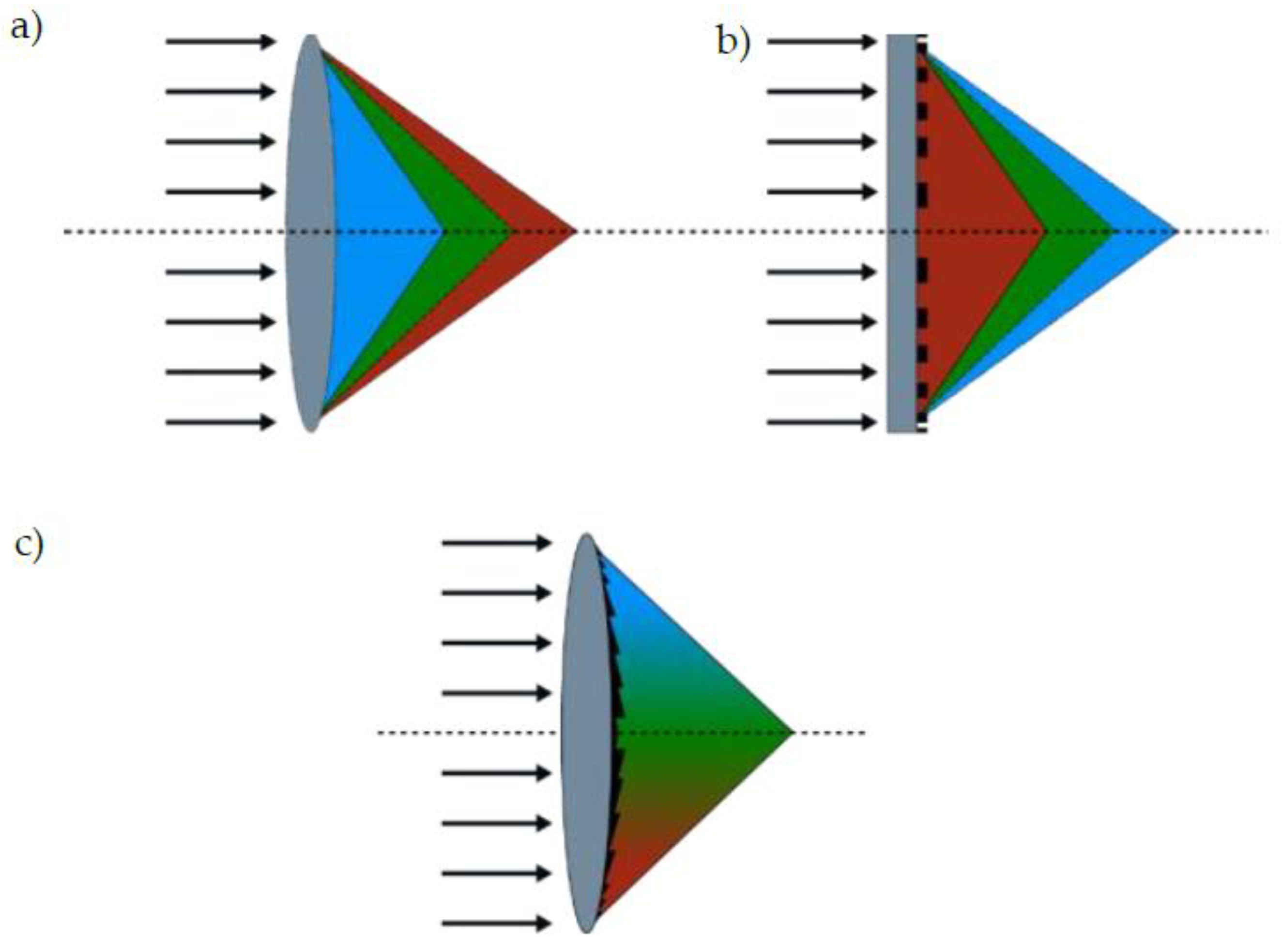
1. Introduction
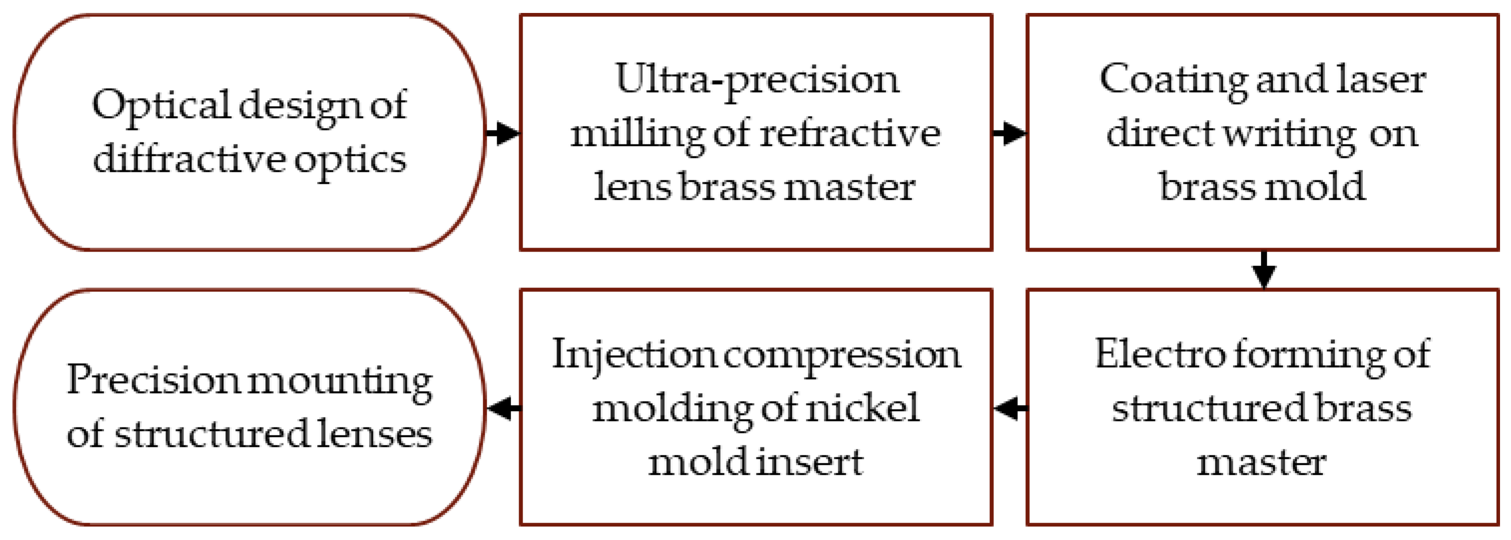
2. Materials and Methods
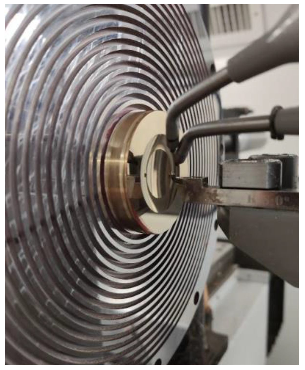
2.1. Ultra-Precision Turning of the Master Structures
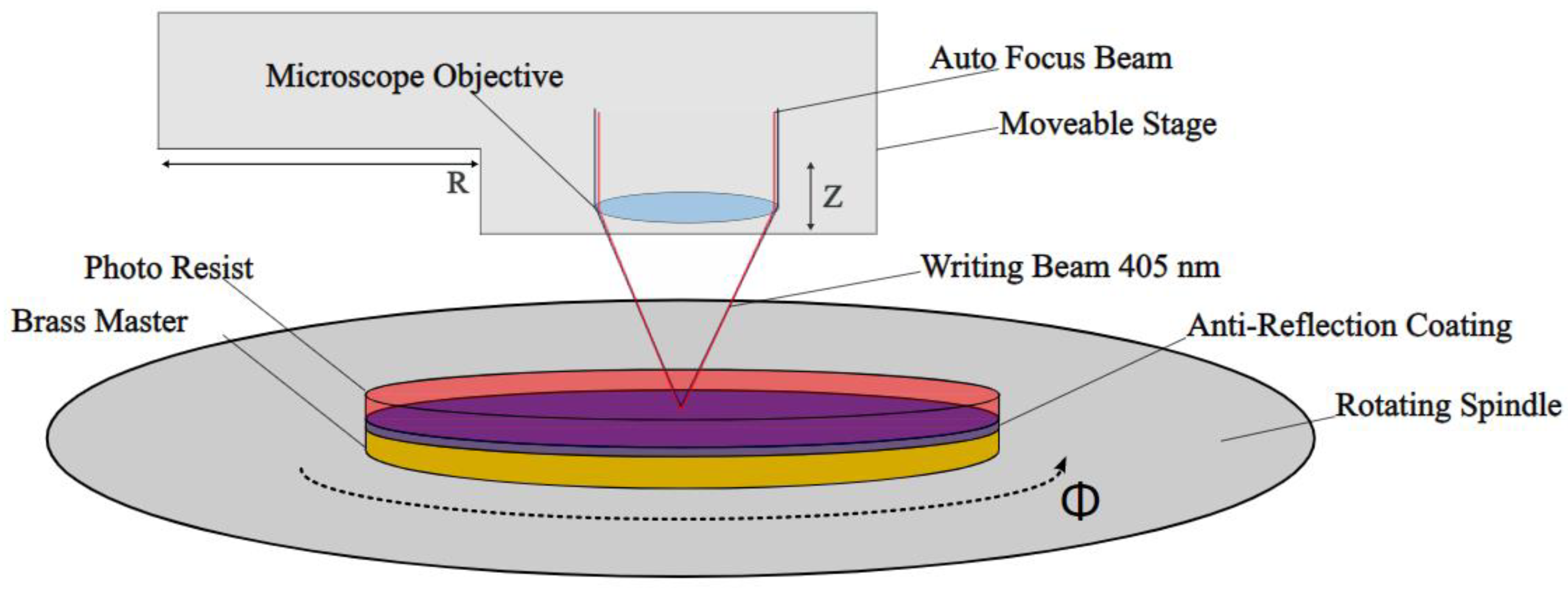
2.2. Laser Direct Writing of Metallic Master Substrates
2.3. Electroforming of Structured Master Substrates
2.4. Injection Compression Molding with Structured Mold Inserts
2.5. Alignment of Polymer Lens Components
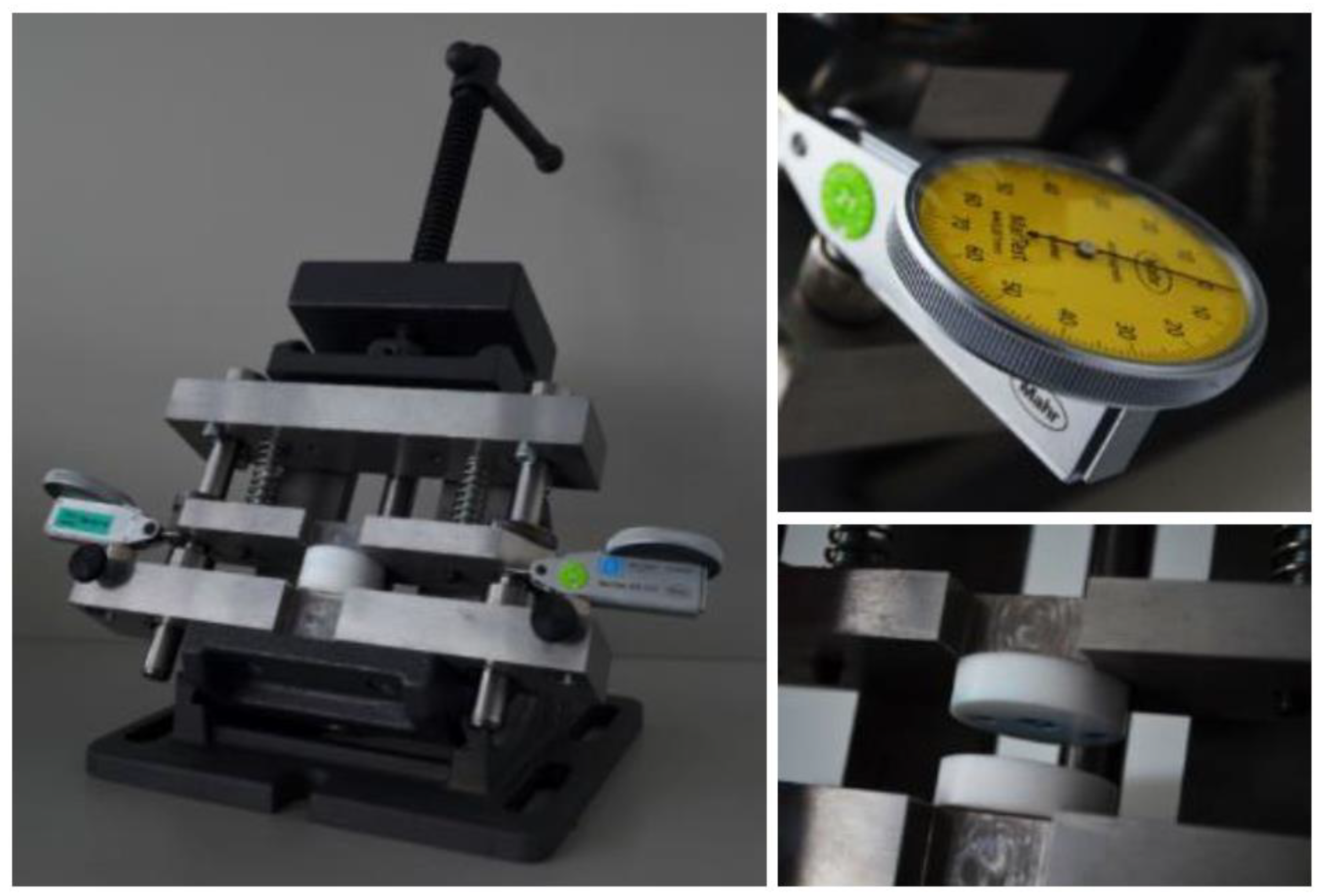
2.6. Process Monitoring
3. Results
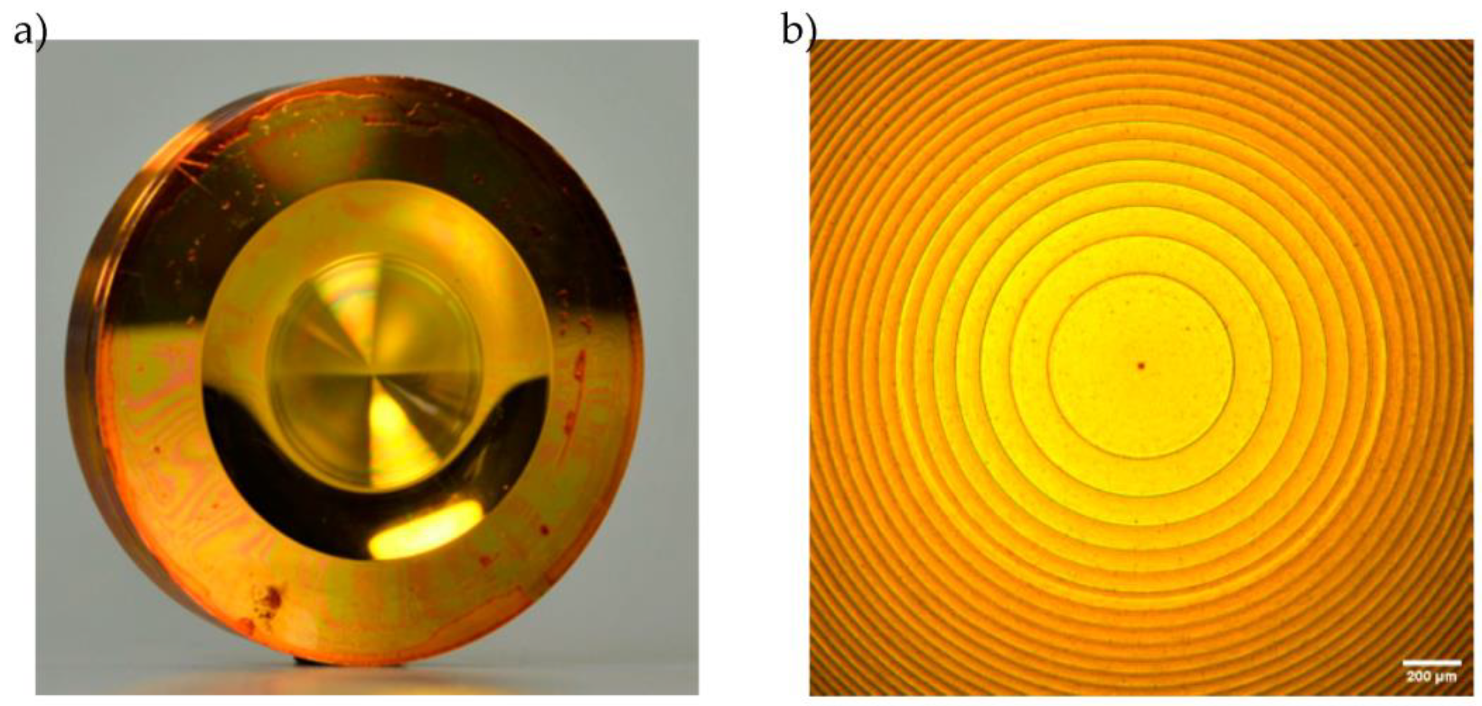
3.1. Ultra-Precision Turning and Laser Direct Writing of the Master Structures
3.2. Electroforming of the Substrate
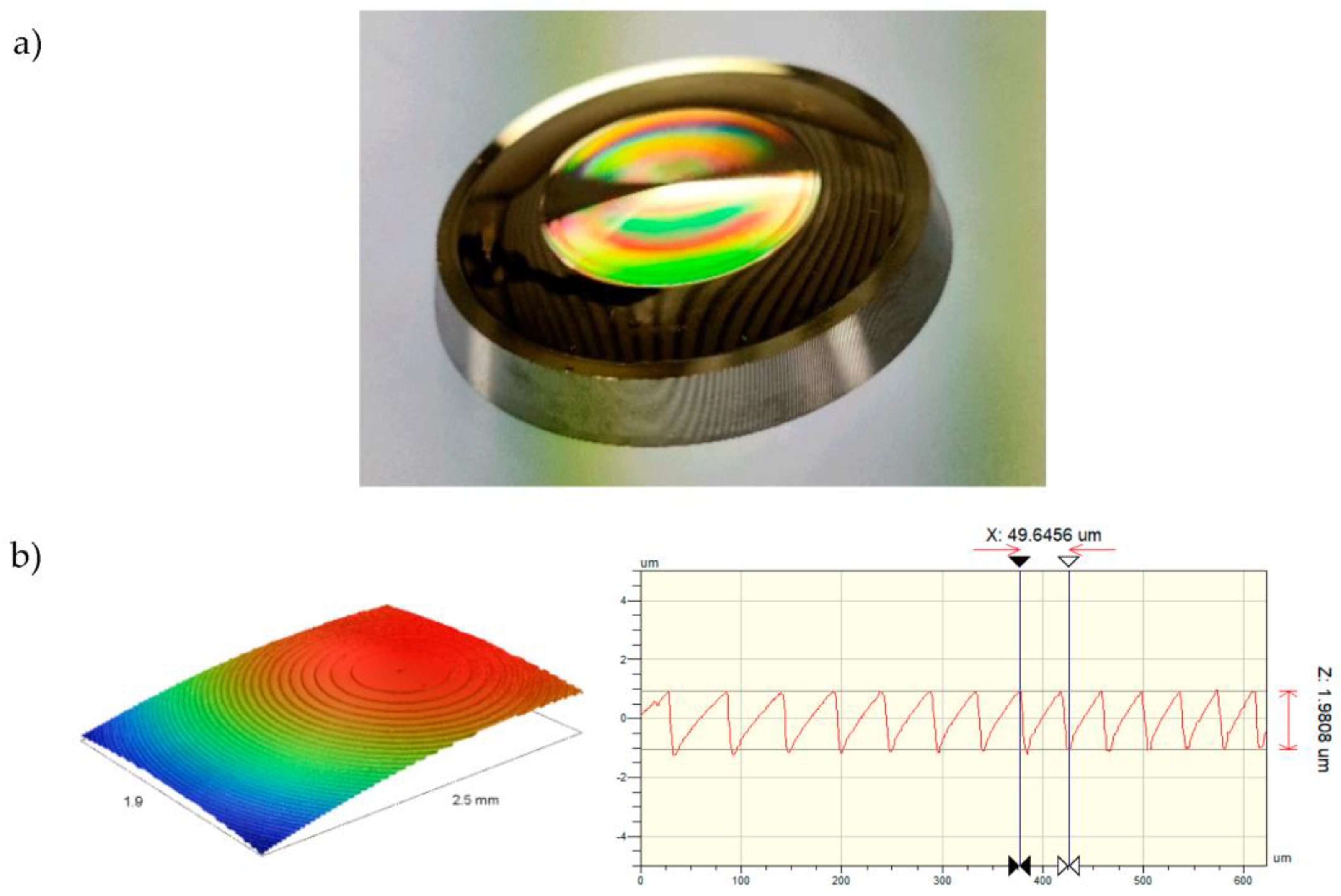
3.3. Injection Compression Molding of Polymeric Optical Elements
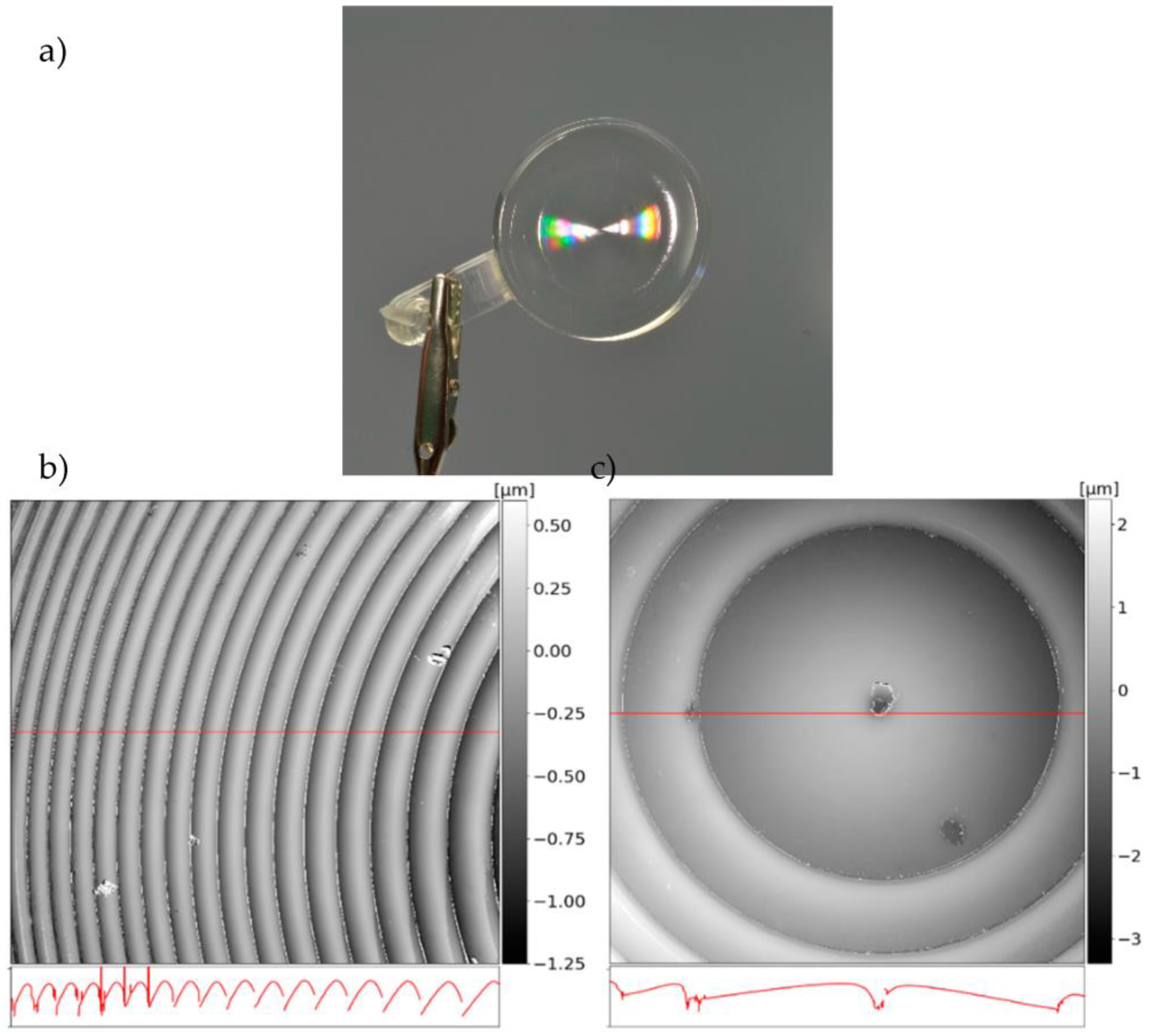
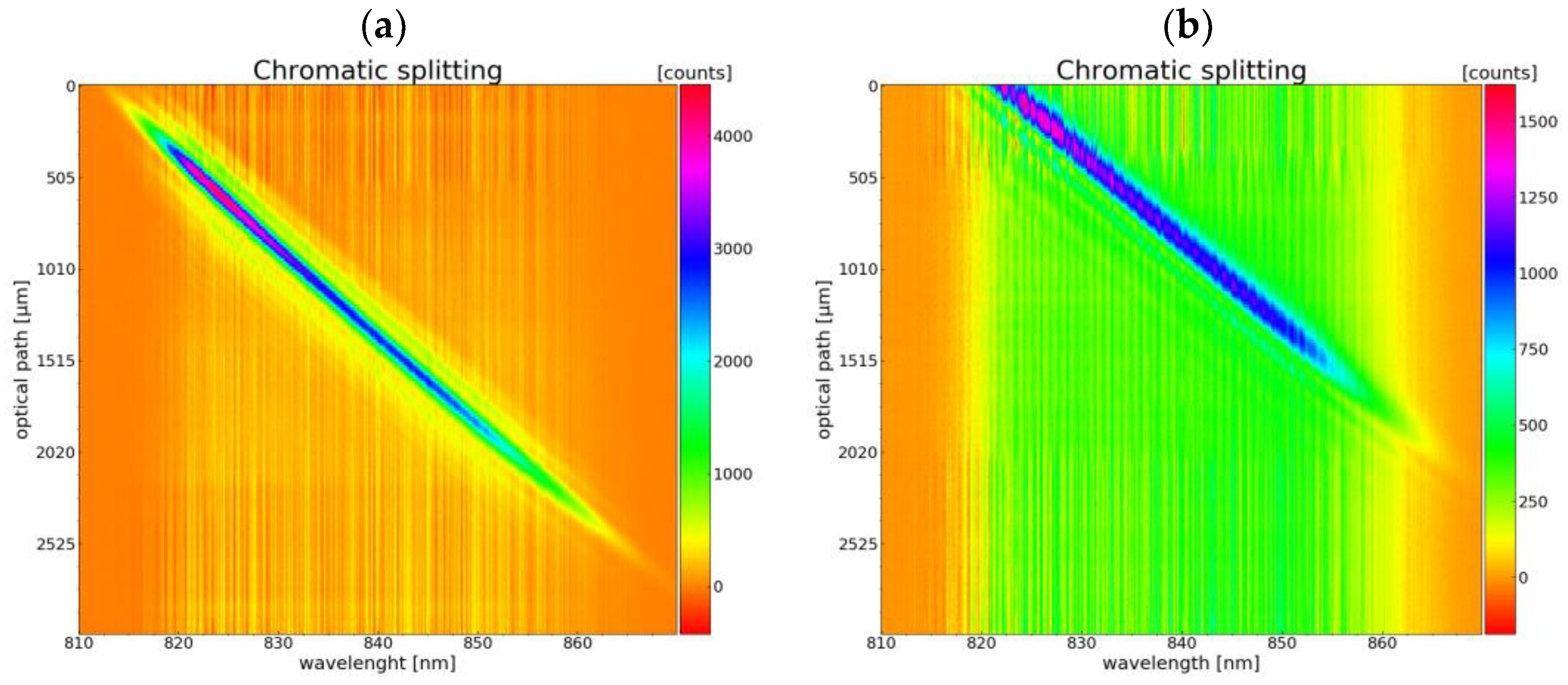
3.4. Optical Measurements
4. Discussion
5. Conclusions
- Overcoming the high initial costs results in the possibility of the flexible production of microstructured optics as different optical microstructures such as gratings, Fresnel structures, or DOEs can be transferred into the mold surface using laser direct writing followed by electro plating.
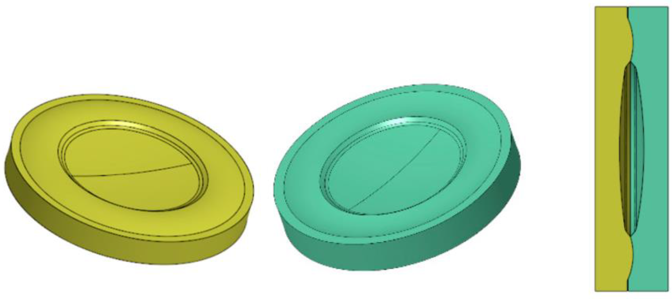
- The manufacturing of zero refractive elements using the suggested process chain has been proven successfully by transferring diffractive microstructures into the curved surface of refractive optics and encapsulating these via alignment structures integrated in the lens system.
- An initial approach for self-alignment during the adjustment of polymer lenses was presented as well. While the alignment structures integrated in the lens system were produced successfully in one step together with the lenses, the adjustment after production requires further investigation.
Author Contributions
Funding
Data Availability Statement
Acknowledgments
Conflicts of Interest
References
- Steinich, T.; Blahnik, V. Optical Design of Camera Optics for Mobile Phones. Adv. Opt. Technol. 2012, 1, 51–58. [Google Scholar] [CrossRef]
- Chesworth, A.A.; Huddleston, J. Precision Optical Components for Lidar Systems Developed for Autonomous Vehicles. In Proceedings of the Next-Generation Optical Communication: Components, Sub-Systems, and Systems VII, San Francisco, CA, USA, 29–31 January 2018; Volume 10561, p. 93. [Google Scholar]
- Kirschmann, M.A.; Pierer, J.; Steinecker, A.; Schmid, P.; Erdmann, A. Plenoptic Inspection System for Automatic Quality Control of MEMS and Microsystems. In Smart Technologies for Precision Assembly, Proceedings of the 9th IFIP WG 5.5 International Precision Assembly Seminar, IPAS 2020, Virtual Event, 14–15 December 2020; Ratchev, S., Ed.; Springer International Publishing: Cham, Switzerland, 2021; pp. 220–232. [Google Scholar]
- Evdokimova, V.V.; Podlipnov, V.V.; Ivliev, N.A.; Petrov, M.V.; Ganchevskaya, S.V.; Fursov, V.A.; Yuzifovich, Y.; Stepanenko, S.O.; Kazanskiy, N.L.; Nikonorov, A.V.; et al. Hybrid Refractive-Diffractive Lens with Reduced Chromatic and Geometric Aberrations and Learned Image Reconstruction. Sensors 2023, 23, 415. [Google Scholar] [CrossRef] [PubMed]
- Chen, W.T.; Zhu, A.Y.; Sisler, J.; Huang, Y.-W.; Yousef, K.M.A.; Lee, E.; Qiu, C.-W.; Capasso, F. Broadband Achromatic Metasurface-Refractive Optics. Nano Lett. 2018, 18, 7801–7808. [Google Scholar] [CrossRef] [PubMed]
- Flores, A.; Wang, M.R.; Yang, J.J. Achromatic Hybrid Refractive-Diffractive Lens with Extended Depth of Focus. Appl. Opt. 2004, 43, 5618–5630. [Google Scholar] [CrossRef] [PubMed]
- Katyl, R.H. Compensating Optical Systems. Part1: Broadband Holographic Reconstruction. Appl. Opt. 1972, 11, 1241–1247. [Google Scholar] [CrossRef]
- Stone, T.; George, N. Hybrid Diffractive-Refractive Lenses and Achromats. Appl. Opt. 1988, 27, 2960–2971. [Google Scholar] [CrossRef]
- Roeder, M.; Drexler, M.; Rothermel, T.; Meissner, T.; Guenther, T.; Zimmermann, A. Injection Compression Molded Microlens Arrays for Hyperspectral Imaging. Micromachines 2018, 9, 355. [Google Scholar] [CrossRef]
- Li, J.; Thiele, S.; Quirk, B.C.; Kirk, R.W.; Verjans, J.W.; Akers, E.; Bursill, C.A.; Nicholls, S.J.; Herkommer, A.M.; Giessen, H.; et al. Ultrathin Monolithic 3D Printed Optical Coherence Tomography Endoscopy for Preclinical and Clinical Use. Light Sci. Appl. 2020, 9, 124. [Google Scholar] [CrossRef]
- Asadollahbaik, A.; Thiele, S.; Weber, K.; Kumar, A.; Drozella, J.; Sterl, F.; Herkommer, A.M.; Giessen, H.; Fick, J. Highly Efficient Dual-Fiber Optical Trapping with 3D Printed Diffractive Fresnel Lenses. ACS Photonics 2020, 7, 88–97. [Google Scholar] [CrossRef]
- Khan, M.S.; Saeed, W.M.; Roth, B.; Lachmayer, R. Diffractive Optics Based Automotive Lighting System: A Rear End Lamp Design for Communication between Road Users. Adv. Opt. Technol. 2021, 10, 49–57. [Google Scholar] [CrossRef]
- Kotz, F.; Arnold, K.; Bauer, W.; Schild, D.; Keller, N.; Sachsenheimer, K.; Nargang, T.M.; Richter, C.; Helmer, D.; Rapp, B.E. Three-Dimensional Printing of Transparent Fused Silica Glass. Nature 2017, 544, 337. [Google Scholar] [CrossRef]
- Mader, M.; Schlatter, O.; Heck, B.; Warmbold, A.; Dorn, A.; Zappe, H.; Risch, P.; Helmer, D.; Kotz, F.; Rapp, B.E. High-Throughput Injection Molding of Transparent Fused Silica Glass. Science 2021, 372, 182–186. [Google Scholar] [CrossRef]
- Roeder, M.; Schilling, P.; Hera, D.; Guenther, T.; Zimmermann, A. Influences on the Fabrication of Diffractive Optical Elements by Injection Compression Molding. J. Manuf. Mater. Process. 2018, 2, 5. [Google Scholar] [CrossRef]
- Zhang, H.; Zhang, N.; Han, W.; Gilchrist, M.D.; Fang, F. Precision Replication of Microlens Arrays Using Variotherm-Assisted Microinjection Moulding. Precis. Eng. 2021, 67, 248–261. [Google Scholar] [CrossRef]
- Gao, P.; Liang, Z.; Wang, X.; Zhou, T.; Xie, J.; Li, S.; Shen, W. Fabrication of a Micro-Lens Array Mold by Micro Ball End-Milling and Its Hot Embossing. Micromachines 2018, 9, 96. [Google Scholar] [CrossRef]
- Klocke, F.; Dambon, O.; Bulla, B.; Heselhaus, M. Direct Diamond Turning of Steel Molds for Optical Replication. In Proceedings of the 4th International Symposium on Advanced Optical Manufacturing and Testing Technologies: Advanced Optical Manufacturing Technologies; International Society for Optics and Photonics, Chengdu, China, 20 May 2009; Volume 7282, p. 728202. [Google Scholar]
- Holthusen, A.-K.; Riemer, O.; Schmütz, J.; Meier, A. Mold Machining and Injection Molding of Diffractive Microstructures. J. Manuf. Process. 2017, 26, 290–294. [Google Scholar] [CrossRef]
- Yoo, D.-Y.; Lee, S.-K.; Lee, D.-H. Ultraprecision Machining-Based Micro-Hybrid Lens Design for Micro Scanning Devices. Int. J. Precis. Eng. Manuf. 2015, 16, 639–646. [Google Scholar] [CrossRef]
- Vallejo-Melgarejo, L.D.; Reifenberger, R.G.; Newell, B.A.; Narváez-Tovar, C.A.; Garcia-Bravo, J.M. Characterization of 3D-Printed Lenses and Diffraction Gratings Made by DLP Additive Manufacturing. Rapid Prototyp. J. 2019, 25, 1684–1694. [Google Scholar] [CrossRef]
- Aguiam, D.E.; Santos, J.D.; Silva, C.; Gentile, F.; Ferreira, C.; Garcia, I.S.; Cunha, J.; Gaspar, J. Fabrication and Optical Characterization of Large Aperture Diffractive Lenses Using Greyscale Lithography. Micro Nano Eng. 2022, 14, 100111. [Google Scholar] [CrossRef]
- Haefner, M.; Pruss, C.; Osten, W. Laser Direct Writing of Rotationally Symmetric High-Resolution Structures. Appl. Opt. 2011, 50, 5983–5989. [Google Scholar] [CrossRef]
- Fu, Y.; Bryan, N.K.A. Hybrid Microdiffractive–Microrefractive Lens with a Continuous Relief Fabricated by Use of Focused-Ion-Beam Milling for Single-Mode Fiber Coupling. Appl. Opt. 2001, 40, 5872–5876. [Google Scholar] [CrossRef] [PubMed]
- Wang, H.; Wang, H.; Zhang, W.; Yang, J.K.W. Toward Near-Perfect Diffractive Optical Elements via Nanoscale 3D Printing. ACS Nano 2020, 14, 10452–10461. [Google Scholar] [CrossRef] [PubMed]
- Gonzalez-Hernandez, D.; Varapnickas, S.; Bertoncini, A.; Liberale, C.; Malinauskas, M. Micro-Optics 3D Printed via Multi-Photon Laser Lithography. Adv. Opt. Mater. 2023, 11, 2201701. [Google Scholar] [CrossRef]
- Radtke, D.; Zeitner, U.D. Laser-Lithography on Non-Planar Surfaces. Opt. Express 2007, 15, 1167–1174. [Google Scholar] [CrossRef] [PubMed]
- Senegačnik, M.; Gregorčič, P. Diffraction-Driven Laser Surface Nanostructuring: Towards Patterning with Curved Periodic Surface Structures. Appl. Surf. Sci. 2023, 610, 155486. [Google Scholar] [CrossRef]
- Schober, C.; Pruss, C.; Herkommer, A.; Osten, W. The NPMM-200: Large Area High Resolution for Freeform Surface Measurement. Proceeding 2020, 11478, 1147807. [Google Scholar] [CrossRef]
- Roeder, M.; Thiele, S.; Hera, D.; Pruss, C.; Guenther, T.; Osten, W.; Zimmermann, A. Fabrication of Curved Diffractive Optical Elements by Means of Laser Direct Writing, Electroplating, and Injection Compression Molding. J. Manuf. Process. 2019, 47, 402–409. [Google Scholar] [CrossRef]
- Rytka, C. Replication of Functional Polymeric Micro- and Nanostructures. Ph.D. Dissertation, Technical University Dortmund, Dortmund, Germany, 2016. [Google Scholar] [CrossRef]
- Evonik Industries. Evonik Industries TROGAMID MyCX 2017; Evonik Industries: Essen, Germany, 2017. [Google Scholar]
- Li, L.H.; Chan, C.Y.; Lee, W.B.; Liu, Y.H. A Novel Evaluation and Compensation Method for Ultra-Precision Machining of Hybrid Lens. Precis. Eng. 2016, 43, 10–23. [Google Scholar] [CrossRef]
- Meier, A. Diamond Turning of Diffractive Microstructures. Precis. Eng. 2015, 42, 253–260. [Google Scholar] [CrossRef]


| Parameter | Value |
|---|---|
| Feed rate [F] | 3.0 |
| Spindle speed [RPM] | 2500 |
| Infeed—roughing [µm] | 0.003 |
| Infeed—finish [µm] | 0.001 |
| Coolant | Isoparafin |
| Parameter | Value |
|---|---|
| Spin time [s] | 30 |
| Acceleration [1/s2] | 800 |
| Spinning speed [RPS] | 1000 |
| Parameter | Value |
|---|---|
| Spin time [s] | 30 |
| Acceleration [1/s2] | 800 |
| Spinning speed [RPS] | 1500 |
| Parameter | Value |
|---|---|
| Melt temperature | 290 °C |
| Mold temperature | |
| Fixed side | 80 °C |
| Moveable side | 80 °C |
| Compression force | 20 kN |
| Cooling time | 25 s |
| Holding pressure | 100 bar |
Disclaimer/Publisher’s Note: The statements, opinions and data contained in all publications are solely those of the individual author(s) and contributor(s) and not of MDPI and/or the editor(s). MDPI and/or the editor(s) disclaim responsibility for any injury to people or property resulting from any ideas, methods, instructions or products referred to in the content. |
© 2023 by the authors. Licensee MDPI, Basel, Switzerland. This article is an open access article distributed under the terms and conditions of the Creative Commons Attribution (CC BY) license (https://creativecommons.org/licenses/by/4.0/).
Share and Cite
Wagner, S.; Treptow, K.; Weser, S.; Drexler, M.; Sahakalkan, S.; Eberhardt, W.; Guenther, T.; Pruss, C.; Herkommer, A.; Zimmermann, A. Injection Molding of Encapsulated Diffractive Optical Elements. Micromachines 2023, 14, 1223. https://doi.org/10.3390/mi14061223
Wagner S, Treptow K, Weser S, Drexler M, Sahakalkan S, Eberhardt W, Guenther T, Pruss C, Herkommer A, Zimmermann A. Injection Molding of Encapsulated Diffractive Optical Elements. Micromachines. 2023; 14(6):1223. https://doi.org/10.3390/mi14061223
Chicago/Turabian StyleWagner, Stefan, Kevin Treptow, Sascha Weser, Marc Drexler, Serhat Sahakalkan, Wolfgang Eberhardt, Thomas Guenther, Christof Pruss, Alois Herkommer, and André Zimmermann. 2023. "Injection Molding of Encapsulated Diffractive Optical Elements" Micromachines 14, no. 6: 1223. https://doi.org/10.3390/mi14061223
APA StyleWagner, S., Treptow, K., Weser, S., Drexler, M., Sahakalkan, S., Eberhardt, W., Guenther, T., Pruss, C., Herkommer, A., & Zimmermann, A. (2023). Injection Molding of Encapsulated Diffractive Optical Elements. Micromachines, 14(6), 1223. https://doi.org/10.3390/mi14061223