Abstract
Biosensors based on tunnel FET for label-free detection in which a nanogap is introduced under gate electrode to electrically sense the characteristics of biomolecules, have been studied widely in recent years. In this paper, a new type of heterostructure junctionless tunnel FET biosensor with an embedded nanogap is proposed, in which the control gate consists of two parts, namely the tunnel gate and auxiliary gate, with different work functions; and the detection sensitivity of different biomolecules can be controlled and adjusted by the two gates. Further, a polar gate is introduced above the source region, and a P+ source is formed by the charge plasma concept by selecting appropriate work functions for the polar gate. The variation of sensitivity with different control gate and polar gate work functions is explored. Neutral and charged biomolecules are considered to simulate device-level gate effects, and the influence of different dielectric constants on sensitivity is also researched. The simulation results show that the switch ratio of the proposed biosensor can reach 109, the maximum current sensitivity is 6.91 × 10², and the maximum sensitivity of the average subthreshold swing (SS) is 0.62.
1. Introduction
Biosensors based on metal oxide semiconductor field effect transistors (MOSFETs) are very popular for label-free detection due to their compactness and energy efficiency, especially the possibility of on-chip integration. The electrical detection principle behind field effect transistor (FET) biosensors is dielectric modulation, in which an electrical nanogap is created under a gate electrode. Dielectric modulated field effect transistors (DM-FETs) can detect not only charged biomolecules but also uncharged biomolecules since the effective capacitance under the gate will be influenced by the charge of biomolecules. As a result, the channel conductance in DM-FETs varies with the variation of detection targets, and the electrical variation can be further processed by measurement systems. In N-type FETs, positively charged molecules will lead to the accumulation of electrons on the sensing channel, resulting in an increase in device conductance, and negatively charged targets will decrease the electron concentration and restrain the device conductance. In P-type FETs, the conclusion is reversed [1,2]. However, MOSFET biosensors are limited by the 60-mV/Dec subthreshold swing (SS), and they have long response times in applications. Tunnel field effect transistors (TFETs), working on band to band tunneling (BTBT) mechanisms, can overcome this limitation, and the fabrication processes for them are compatible with conventional CMOS. Many researchers have reported TFET-based biosensors, which can ensure high sensitivity and low power consumption in applications for biomolecule detection [3,4]. The sensitivity of TFET-based biosensors can be evaluated by changes in electrical parameters caused by permittivity variation in charged or uncharged biomolecules, such as drain current, threshold voltage, subthreshold swing, etc. [5,6].
However, TFET-based biosensors already exist that need ultra-steep doping profiles in active regions to form abrupt junctions, leading to random dopant fluctuations (RDFs). Moreover, the quantum tunneling barrier width between the source and the channel interface in conventional TFET biosensors will significantly affect the ON-state current.
To overcome stringent demands of fabrication and avoid high thermal budgets in conventional TFETs, the junctionless tunneling field effect transistor (JLTFET) has been extensively studied in recent years [7,8,9,10]. Fabricating abrupt metallurgical junctions at high temperatures is not necessary with JLTFETs, in which uniformly high-doping concentrations are adopted in the source, channel, and drain regions. Moreover, the source and drain regions in JLTFETs are formed by the charge plasma concept, in which appropriate work functions for electrodes are chosen to further avoid a high thermal budget [11,12,13,14,15].
In this article, we propose a dual material gate heterostructure junctionless tunneling field effect transistor (DMG-HJLTFET) biosensor for the first time [16,17,18,19,20,21,22]. The proposed DMG-HJLTFET biosensor has three novel aspects. First, the control gate is divided into two parts, namely the tunnel gate and auxiliary gate, using a gate-engineered concept, in which the work functions of the tunnel gate and auxiliary gate are carefully optimized to obtain high current sensitivity and a high switch ratio. Second, an optimized InAs/GaAs0.5Sb0.5 heterostructure is adopted between the source and the channel interface, which can effectively narrow the tunneling barrier width in this region due to the properties of III-V compound semiconductor materials. Third, the charge plasma concept is used to form P+-I-N+ structures by selecting appropriate work functions for the polar gate (PG) and control gate (CG), which can avoid the formation of abrupt junctions due to uniform doping concentrations in this kind of device. Nanogaps are located below the TGs, and charged or uncharged biomolecules will lead to gate effects when they enter these gaps [23,24,25,26,27,28].
2. Geometric Structure and Simulation
Figure 1a shows the cross-sectional view of the DMG-HJLTFET biosensor. As can be seen from Figure 1a, a GaAs0.5Sb0.5 (0.5 is the optimized value, which we analyze later) pocket structure is introduced between the source and the channel, which can effectively enhance the tunneling rate in this region [20]. The control gate electrode consists of a TG and an AG using two different metals. The ON-state current and the OFF-state current of the DMG-HJLTFET biosensor can be optimized by choosing appropriate work functions for the TG and AG. HfO2 as a dielectric material under the TG is etched out to form a nanogap for biosensing purposes. The charge plasma concept is used to form the source region, which is controlled by the PG. All the regions adopt uniform doping concentrations.
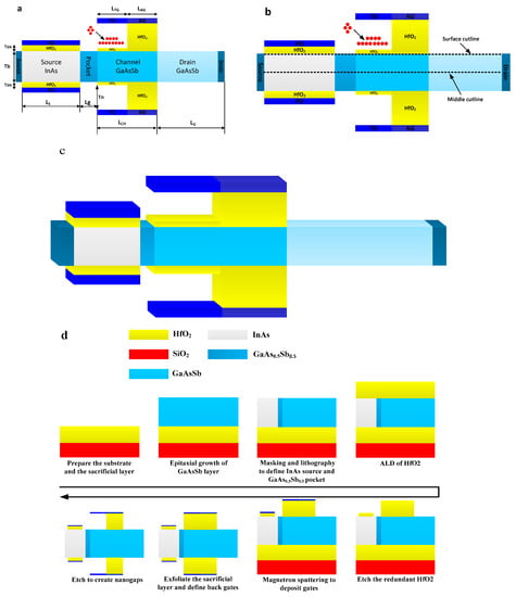
Figure 1.
(a) Cross-sectional view of DMG-HJLTFET biosensor; (b) section diagram of cutting lines; (c) 3-D graphic of DMG-HJLTFET; (d) tentative fabrication flow of DMG-HJLTFET.
The length of the proposed device is 67 nm, and detailed parameters are listed in Table 1.

Table 1.
The fundamental geometrical and physical parameters of the DMG-HJLTFET.
We simulate the proposed device in ATLAS Silvaco TCAD software, version 5.20.2.R. The nonlocal BTBT model (BBT.NONLOCAL) is activated to consider forward and reverse tunneling currents. To include the effects caused by high doping and thinner oxide, Hansch’s quantum confinement model (HANSCHQM) is activated. We also activate the Schenk model for tunneling (SCHENK.TUN), the Fermi statistics (FERMI) model, and the band gap narrowing (BGN) model, and we refine the simulation mesh and select the simulation method with better convergence.
It is worth emphasizing that a dual material gate structure can be realized by the molecular beam epitaxy (MBE) method, using the method in article [25]. Moreover, a III-V compound structure can be fabricated by the metal organic chemical vapor deposition (MOCVD) method [27,28,29]. Figure 1c shows a 3-D graphic of the DMG-HJLTFET, and Figure 1d shows the tentative fabrication flow for the DMG-HJLTFET.
The presence of biomolecules will alter the dielectric constant of the nanogaps, and these nanogaps in our simulation are occupied by insulating material with the same dielectric constant as the corresponding biomolecule. In addition, the charges of biomolecules are considered to be interface states between HfO2 and the equivalent material. Although no experimental results are available for this kind of TFET biosensor, based on experimental data and theoretical calculations, the dielectric modulated double gate tunnel field effect transistor (DG-TFET) biomolecule sensor in reference [12] is well calibrated. Therefore, the BTBT model in this article is calibrated by reproducing the results reported in [12], as shown in Figure 2a.
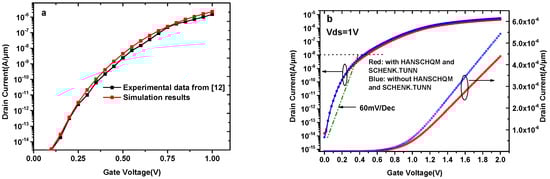
Figure 2.
(a) Simulation models calibrated by reproducing the results of [12]. (b) Transfer characteristics of DMG-HJLTFET biosensor with and without HANSCHQM and SCHENK.TUN.
Figure 2b shows the transfer characteristics of the DMG-HJLTFET biosensor with and without HANSCHQM and SCHENK.TUN. In this condition, nanogaps are occupied by air (k = 1). To consider trap-assisted tunneling, the SCHENK.TUN model is activated in our simulation. This model gives the field-effect enhancement factors as an analytic function, and Atlas works out this function through several intermediate quantities. Moreover, it is necessary to consider the effects near the oxide interface because the minimum oxide layer thickness in our simulation is as small as a few nanometers, and HANSCHQM is suitable for accurate simulations of quantum mechanical confinement effects near the gate oxide interface. As can be clearly seen from this figure, the two models have a significant effect on both OFF-state current (Vgs = 0 V) and ON-state current (Vgs = 2 V). The maximum ON-state current with HANSCHQM and SCHENK.TUN is 4.39 × 10⁻⁶ A/μm, and the switch ratio can reach 109, while the average SS is 82mV/Dec.
Figure 3a and b show the ON-state and OFF-state energy band diagram of DMG-HJLTFET (k = 1), respectively, which explain the reason for maintaining a high ON-state current and switch ratio. It is found that the valance band and conduction band between the source and channel are very close to each other, ensuring a smaller tunneling distance at the surface region, as shown by t1. At the same time, tunneling distance at the middle region, represented by t2, is not very large, so the middle region also contributes a small amount to the tunneling current. The tunneling width and effective tunneling area at the surface and middle region in this biosensor are distinctly improved by InAs/GaAs0.5Sb0.5 heterostructures. Moreover, the TG with a work function of ΦM1 can lower the minimum value of the conduction band at the pocket region, which can further improve the tunnel process in this region; the AG with a work function of ΦM2 can produce an extra barrier in the channel region, which can help to improve the OFF-state current and switch ratio. In Figure 3b, we can see that the tunneling distance of the conduction band and valance band at the source/channel interface in both regions is too large to tunnel effectively.
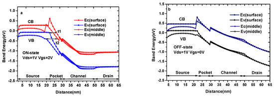
Figure 3.
(a) The ON-state energy band diagram of DMG-HJLTFET; (b) The OFF-state energy band diagram of DMG-HJLTFET.
Obviously, the current capacity of the DMG-HJLTFET will be affected by the composition variation in GaAsySb1-y, and GaAs0.5Sb0.5 is an optimized value.
In Figure 4, we depict the transfer characteristics and energy band diagram of a DMG-HJLTFET with a different y. As can be seen in Figure 4a, both the ON-state current (Vgs = 2.0 V) and the OFF-state current (Vgs = 0 V) decrease with the increase in y, and the OFF-state current is close to 10−14 A/μm until y.comp = 0.5. For the sake of compromise, we choose y.comp = 0.5. Figure 4b shows the ON-state energy band diagram of the DMG-HJLTFET with a different y. It is found that the value of the conduction band in the GaAsySb1−y region increases with the increase in y, while the valance band changes in the opposite direction, indicating a reduction in the effective tunneling area at the source/pocket interface. The OFF-state energy band diagram of the DMG-HJLTFET with a different y is similar to that of the ON-state diagram. However, there are still significant electrons that can tunnel from the source to the pocket due to the small tunneling distance when y.comp<0.5. Therefore, the variation of energy bands leads to the change in current in Figure 4a.
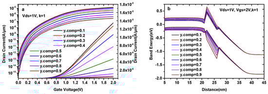
Figure 4.
(a) Transfer characteristics of DMG-HJLTFET and (b) energy band diagram of DMG-HJLTFET with different y in GaAsySb1−y.
3. Results and Discussion
3.1. Influence of Tunnel Gate Work Function
Formula (1) gives the current sensitivity for biosensors:
In this paper, we continue to use this definition. ID,k and ID,air represent the drain current of the DMG-HJLTFET biosensor with biomolecules and without biomolecules, respectively.
Figure 5a–c indicate the transfer characteristics and the energy band diagrams of the DMG-HJLTFET with different tunnel gate work functions (ΦM1), wherein we keep k = 12, ΦM2 = 3.9eV and ΦPG = 5.9 eV. As shown in Figure 5a, the selection of ΦM1 is crucial for obtaining a higher Ion/Ioff and a lower average SS. Although the ON-state current gradually decreases with the increase in ΦM1, the switch ratio and SS value are very poor when ΦM1<4.3 eV.
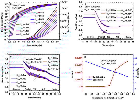
Figure 5.
(a) Transfer characteristics of DMG-HJLTFET; (b) the variation of the ON-state energy band diagram; (c) the variation of the OFF-state energy band diagram; and (d) sensitivity and switch ratios (k = 12) with different tunnel gate work functions (ΦM1).
In Figure 5b, it is observed that the tunneling effective area decreases with the increase in ΦM1, consistent with the variation of the maximum ON-state current in Figure 5a. The mechanism of OFF-state current variation can be explained by the OFF-state energy band diagram in Figure 5c. There is overlap between the source valance band and the pocket conduction band before ΦM1 = 4.3 eV; i.e., the tunneling process still exists when ΦM1<4.3 eV, resulting in high Ioff in these conditions, while the overlap disappears after ΦM1 = 4.3 eV, causing the OFF-state current to become very small, as shown in Figure 5a.
Figure 5d indicates the variations in sensitivity (k = 12) and switch ratio with different tunnel gate work functions. The surface potential and electric field under the tunnel gate decrease with the increase in ΦM1, leading to the elevation of the conduction band and valance band in the pocket region, and this trend becomes more obvious with the increase in ΦM1. As a result, the tunneling effective area decreases with the increase in ΦM1; in other words, ID,k decreases with the increase in ΦM1. Therefore, the sensitivity decreases with the increase in ΦM1. As can be seen in Figure 5d, the sensitivity of the DMG-HJLTFET decreases from 35.76 to 15.89 when ΦM1 increases from 3.8 eV to 4.5 eV, whereas the switch ratio is greater than 109 after ΦM1 = 4.3 eV. Therefore, the optimal work function value for the TG is chosen as 4.3 eV. To gain insight into the design and optimization process of the TG, the detailed variation of the sensitivity and switch ratio with different ΦM1 is shown in Table 2.
Table 2.
The variation in sensitivity and switch ratios with different ΦM1 (Vgs = 2.0 V, Vds = 1.0 V, ΦM2 = 3.9 eV, ΦPG = 5.9 eV).
3.2. Influence of Auxiliary Gate Work Function and Polar Gate Work Function
In this section, we discuss the influence of ΦM2 and ΦPG on electrical performance.
Figure 6a shows the transfer characteristics of a DMG-HJLTFET with different values of ΦM2, where ΦM2 increases from 3.8 eV to 4.5 eV in steps of 0.1 eV. In Figure 6a, it is found that the current at Vgs = 2.0 V decreases with the increase in ΦM2. However, the OFF-state current of ΦM2 = 3.8 eV is 3.79 × 10⁻¹³ A/μm, which is one or two orders of magnitude higher than the OFF-state current in other cases. Figure 6b shows the ON-state and the OFF-state energy band diagram of a DMG-HJLTFET with a different auxiliary gate work function (ΦM2), where it is observed that the valley of conduction band in the pocket region increases with the increase in ΦM2 at Vgs = 2.0 V and Vgs = 0 V. As a result, the ON-state effective tunneling area at the source/pocket interface decreases with the increase in ΦM2, and the OFF-state tunneling distance between the source valance band and the pocket conduction band increases with the increase in ΦM2. Moreover, an overlap between the source valance band and the pocket conduction band exists at ΦM2 = 3.8 eV in the OFF-state. These variations in the energy band are highly consistent with the current change in Figure 6a. Therefore, ΦM2 = 3.9 eV is chosen as the optimal value for the auxiliary gate.
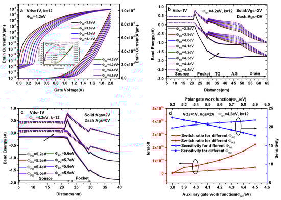
Figure 6.
(a) Transfer characteristics of DMG-HJLTFET with different auxiliary gate work functions (ΦM2); (b) energy band diagram of DMG-HJLTFET with different auxiliary gate work functions (ΦM2); (c) energy band diagram of DMG-HJLTFET with different polar gate work functions (ΦPG); (d) the variation of sensitivity and switch ratios with different ΦM2 and ΦPG.
The inset indicates the transfer characteristics of a DMG-HJLTFET with different values of ΦPG, in which we keep ΦM1 = 4.3 eV and ΦM2 = 3.9 eV. The inset picture shows that the ON-state current at Vgs = 2.0 V gradually increases when ΦPG varies from 5.2 eV to 5.9 eV in steps of 0.1 eV, whereas the OFF-state current is not obviously influenced by ΦPG, which remains on the order of 10−14 A/μm. The reason for this outcome is that the polarization charge forming in the source region is deeply influenced by ΦPG, and the number of polarization charges increases with the increase in ΦPG. Figure 6c illustrates the energy band variation of DMG-HJLTFET with different ΦPG; although the energy band gap among different ΦPG is not obvious at Vgs = 2.0 V, the position of the conduction band and valance band in the source region becomes increasingly higher when ΦPG increases, resulting in the increase in the effective tunneling area at the source/pocket interface.
Additionally, the position of the conduction band and valance band in the source and pocket regions at Vgs = 0 V becomes increasingly higher, ensuring that the OFF-state current decreases with the increase in ΦPG. Because of the ON-state current and OFF-state current, we choose ΦPG = 5.9 eV.
To better understand the influence of the AG and PG, the detailed variation of sensitivity and switch ratios with different ΦM2 are shown in Table 3, and Table 4 shows the variation in sensitivity and switch ratios with different ΦPG.
Table 3.
The variation of sensitivity and switch ratios with different ΦM2 (Vgs = 2.0 V, Vds = 1.0 V, ΦM1 = 4.3 eV, ΦPG = 5.9 eV).
Table 4.
The variation of the sensitivity and switch ratio with different ΦPG (Vgs = 2.0 V, Vds = 1.0 V, ΦM1 = 4.3 eV, ΦM2 = 3.9 eV).
Figure 6d shows the variation in sensitivity and switch ratios (k = 12) with different auxiliary gates and polar gates. The sensitivity decreases from 22.49 to 17.71 when ΦM2 increases from 3.8 eV to 4.5 eV, whereas the switch ratio of ΦM2 = 3.8 eV is only 2.61 × 10⁸. Therefore, the AG work function is chosen as 3.9 eV to account for the ON-state current, switch ratio and sensitivity. The sensitivity increases from 19.70 to 21.87 when ΦPG increases from 5.2 eV to 5.9 eV, and the switch ratio increases from 4.42 × 10⁸ to 4.76 × 10⁹. Therefore, we choose ΦPG = 5.9 eV.
3.3. Influence of Charge Density and Dielectric Constant
The comparison of transfer characteristics with different charge densities is shown in Figure 7a. Figure 7a presents the plots for the positive charge and negative charge at a fixed dielectric constant (k = 1 and k = 12). The ON-sate current of k = 1 is much smaller than that of k = 12 for a certain charge density when ρ increases from −1 × 1012 cm−2 to 1 × 1012 cm−2. For ρ = 1 × 1012 cm−2, the maximum ON-state current rises by a factor of 18.1. The reason for this change is that a higher dielectric constant helps to form a p-type source and an intrinsic channel under uniform doping conditions, resulting more electrons tunneling from the source to the pocket due to an increase in surface potential. Figure 7b shows the variation of sensitivity and switch ratios with different charge densities for k = 1 and k = 12. The sensitivity of k = 1 rises by a factor of 2.28, whereas the switch ratio is reduced by three orders of magnitude when ρ increases from −1 × 1012 cm−2 to 1 × 1012 cm−2. The switch ratio of k = 12 is also reduced by three orders of magnitude, whereas the sensitivity only rises by a factor of 1.18 when ρ increases from −1 × 1012 cm−2 to 1 × 1012 cm−2.
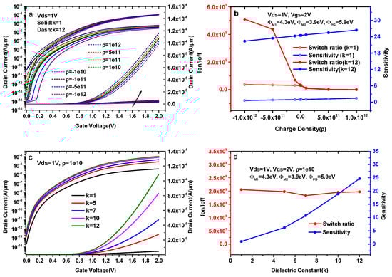
Figure 7.
(a) Transfer characteristics of DMG-HJLTFET for different charge densities with a fixed dielectric (k = 1 and k = 12); (b) the variation of the sensitivity and switch ratio for different charge densities with a fixed dielectric (k = 1 and k = 12); (c) Transfer characteristics of DMG-HJLTFET for k = 1, 5, 7, 10, and 12 at a fixed charge (ρ = 1 × 1010 cm−2); (d) the variation of the sensitivity and switch ratio for k = 1, 5, 7, 10, and 12 at a fixed charge (ρ = 1 × 1010 cm−2).
We know that the voltage balance equation of a metal-oxide-semiconductor structure is:
where ψS is the surface electrostatic potential, ΦMS is the work function difference between the metal and the semiconductor, q is the value of the unit charge, ρ is the number of charged biomolecules per unit area, and Ceff is the resultant capacitance per unit area.
In our simulation, the third term of Formula (2) goes from large to small when ρ increases from −1 × 1012 cm−2 to 1 × 1012 cm−2, indicating that the surface electrostatic potential (ψS) increases with the increase in ρ. Therefore, the tunneling probability near the tunnel gate increases when ρ increases from −1 × 1012 cm−2 to 1 × 1012 cm−2, resulting in an increase in the drain current and sensitivity in this device. In addition, an increase in ρ will enhance the OFF-state current, and the switch ratio decreases with the increase in ρ. In summary, the sensitivity increases and the switch ratio decreases when ρ varies from −1 × 1012 cm−2 to 1 × 1012 cm−2, and the change of sensitivity at a low k is more obvious than that of a high k.
Like the previous section, similar plots for different dielectric constant of biomolecules are presented in Figure 7c at a fixed charge (ρ = 1 × 1010 cm−2). As shown in Figure 7c, both the ON-state current and the OFF-state current increase with the increase in k. The reason for these changes is that equivalent capacitance under the tunnel gate reduces with the increase in the dielectric constant of the biomolecules. Gate effects caused by biomolecules at a fixed charge density become increasingly obvious when k goes from 1 to 12.
As reflected in the transfer characteristics, the ON-state current increases obviously with k, and the maximum ON-state current for k = 12 is 1.1 × 10⁻⁴ A/μm, whereas the maximum ON-state current for k = 1 is only 4.43 × 10⁻⁶ A/μm. The change of the OFF-state current is smaller than that of the ON-state current, and the OFF-state currents for k = 1 and k = 12 are 2.16 × 10⁻¹⁴ A/μm and 5.49 × 10⁻¹³ A/μm, respectively.
Combined with the changes in current capacity, Figure 7d shows the variation of the sensitivity and switch ratios for k = 1, 5, 7, 10, and 12 at ρ = 1 × 1010 cm−2. It is clear that the sensitivity of DMG-HJLTFET biosensor increases from 1.01 to 24.7 when k goes from 1 to 12, and the switch ratio of DMG-HJLTFET biosensor is always on the order of 108.
In fact, compounds having the ability to cause biological interactions possess high dielectric constant, such as acetylene tetrabromide, which causes acute intoxication in a human being if exposed unconditionally and has a dielectric constant of 7; pyridine, which is used widely in agrochemicals; and denatured alcohol, which has a dielectric constant of 13 [23]. Next, we use these two substances to analyze the linearity and selectivity of the proposed device.
Figure 8a compares the current capacity of a DMG-HJLTFET corresponding to different contents of acetylene tetrabromide and pyridine. It is found that the DMG-HJLTFET biosensor shows different selectivity for acetylene tetrabromide and pyridine. The current capacity of the DMG-HJLTFET decreases with the increase in acetylene tetrabromide percentage. The maximum ON-state current is 9.51 × 10⁻⁵ A/μm when the acetylene tetrabromide percentage is 20%, and the maximum ON-state current drops to 5.69 × 10⁻⁵ A/μm when the acetylene tetrabromide percentage increases to 80%. The DMG-HJLTFET shows higher selectivity for materials with high dielectric constants, and materials with higher dielectric constants are easier to detect. Figure 8b indicates the sensitivity with different levels of acetylene tetrabromide and pyridine. The sensitivity is 21.7 when the acetylene tetrabromide percentage is 20%, while the sensitivity is 12.9 when the acetylene tetrabromide percentage is 80%.
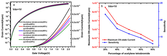
Figure 8.
(a) Transfer characteristics of DMG-HJLTFET for different contents of acetylene tetrabromide and pyridine; (b) the variation of the maximum ON-state current and sensitivity for different contents of acetylene tetrabromide and pyridine.
The SS sensitivity of biosensor is defined as follows:
Figure 9a shows the sensitivity variation of the DMG-HJLTFET biosensor with different LTG. It is very clear that the current sensitivity and SS sensitivity increase with the enhancement of LTG. The values of current sensitivity and SS sensitivity are 6.91 × 10² and 0.62, respectively, when LTG = 50 nm.
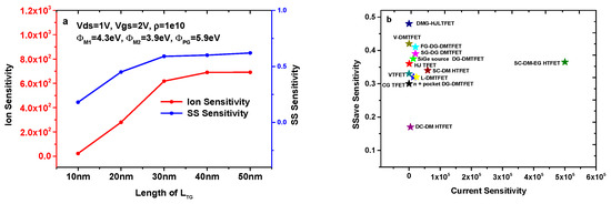
Figure 9.
(a) Ion sensitivity and SS sensitivity for different LTG (k = 12); (b) comparison of different biosensors based on TFET.
Figure 9b compares the sensitivity of different TFET-based biosensors. Details of different TFET-based biosensors are listed in Table 5. In this article, for fairness of comparison, we adopt the same device thickness (10 nm) and device length (100 nm) for these different TFET-based biosensors. It is found that the DMG-HJLTFET possesses the maximum SS sensitivity due to its structural innovation. Although the SC-DM-EG HTFET has a current sensitivity of 5 × 10⁵, the SS sensitivity is clearly less than 0.4. The SS sensitivity of other structures is obviously smaller than that of the DMG-HJLTFET, and their current sensitivity is far less than 5 × 10⁵.
Table 5.
Details of different TFET-based biosensors from Figure 9b.
4. Conclusions
An insightful analysis for a dual material gate heterostructure junctionless tunneling field effect transistor (DMG-HJLTFET) biosensor has been presented in this work. An InAs/GaAsSb heterojunction is adopted between the source and the channel to improve the band-to-band tunneling (BTBT) rate, and a pocket structure formed by GaAs0.5Sb0.5 is inserted to further enhance the electron tunneling process at the source/channel interface. Nanogaps are introduced under the gate electrode to electrically sense the characteristics of biomolecules, and gate effects occur when biomolecules enter the detection position. To obtain higher sensitivity and a higher switch ratio, the gate electrode is divided into two parts, namely the tunnel gate and auxiliary gate; we can improve the ON-state current and the OFF-state current simultaneously by selecting appropriate work functions for the tunnel gate and auxiliary gate. The influences of different tunnel gates on sensitivity and switch ratio are explored in depth. Simulation results show that 4.3 eV is the optimal work function value for TG, and superior values for sensitivity and switch ratio can be obtained in this condition. We also study the effects of auxiliary gate work functions on device performance by keeping ΦM1 = 4.3 eV. ΦM2 = 3.9 eV is selected as the most suitable value for AG. Then, the electrical properties of positive and negative charges at k = 1 and k = 12 are researched, and the results show that the sensitivity increases, the switch ratio decreases with the increase in charge density, and the change in sensitivity at a low k is more obvious than that at a high k. Furthermore, the influence of the dielectric constant on biosensor performance is also compared, and the simulation results show that dielectrically modulated effects caused by biomolecules become increasingly obvious when k goes from 1 to 12.
Author Contributions
Conceptualization, H.L. and H.X.; methodology, H.X.; software, H.X.; validation, H.L. and H.X.; formal analysis, H.X.; investigation, H.X.; resources, H.X.; data curation, H.X.; writing—original draft preparation, H.X.; writing—review and editing, H.X.; visualization, H.X.; supervision, H.X.; project administration, H.L.; funding acquisition, H.L. All authors have read and agreed to the published version of the manuscript.
Funding
This research was funded by the National Natural Science Foundation of China (Grant No. U2241221).
Conflicts of Interest
The authors declare no conflict of interest.
References
- Foad, G.; Abdollah, S. Advances in 2D-based Field-effect transistors as biosensing platforms: From principle to biomedical applications. Microchem. J. 2023, 187, 108432. [Google Scholar]
- Vu, C.-A.; Chen, W.-Y. Field-Effect Transistor Biosensors for Biomedical Applications: Recent Advances and Future Prospects. Sensors 2019, 19, 4214. [Google Scholar] [CrossRef] [PubMed]
- Rajamohanan, B.; Pandey, R.; Chobpattan, V.; Vaz, C.; Gundlach, D.; Cheung, K.P.; Suehle, J.; Stemmer, S.; Datta, S. 0.5 V Supply Voltage Operation of In0.65Ga0.35As/GaAs0.4Sb0.6 Tunnel FET. IEEE Electron. Device Lett. 2014, 36, 20–22. [Google Scholar]
- Luo, Z.; Wang, H.; An, N.; Zhu, Z. A Tunnel Dielectric-Based Tunnel FET. IEEE Electron. Device Lett. 2015, 36, 966–968. [Google Scholar] [CrossRef]
- Yang, Y.; Guo, P.; Zhan, C.; Han, G.; Yeo, Y.; Zhou, Q.; Yeo, Y. Silicon-based tunneling field-effect transistor with elevated germanium source formed on (110) silicon substrate. Appl. Phys. Lett. 2011, 98, 153502. [Google Scholar]
- Shaikh, M.R.U.; Loan, S.A. Drain-Engineered TFET With Fully Suppressed Ambipolarity for High-Frequency Application. IEEE Trans. Electron. Devices 2019, 66, 1628–1634. [Google Scholar] [CrossRef]
- Min, J.; Wu, J.; Taur, Y. Analysis of Source Doping Effect in Tunnel FETs With Staggered Bandgap. IEEE Electron. Device Lett. 2015, 36, 1094–1096. [Google Scholar] [CrossRef]
- Faraz, N.; Seopand, Y.Y. Impact of Quantum Confinement on Band-to-Band Tunneling of Line-Tunneling Type L-Shaped Tunnel Field-Effect Transistor. IEEE Trans. Electron. Devices 2019, 66, 2010–2016. [Google Scholar]
- Ranjan, T.M.; Kumar, S.A.; Baral, K.; Singh, P.K.; Jit, S. III-V/Si staggered heterojunction based source-pocket engineered vertical TFETs for low power applications. Superlattices Microstruct. 2020, 142, 106494. [Google Scholar]
- Lee, H.; Park, S.; Lee, Y.; Nam, H.; Shin, C. Random variation analysis and variation-aware design of symmetric tunnel field-effect transistor. IEEE Trans. Electron. Devices 2015, 62, 1778–1783. [Google Scholar]
- Kumar, M.J.; Janardhanan, S. Doping-Less Tunnel Field Effect Transistor: Design and Investigation. IEEE Trans. Electron. Devices 2013, 60, 3285–3289. [Google Scholar] [CrossRef]
- Tahaei, S.H.; Ghoreishi, S.S.; Yousefi, R.; Aderang, H. A computational study of a carbon nanotube junctionless tunneling field-effect transistor (CNT-JLTFET) based on the charge plasma concept. Superlattices Microstruct. 2018, 125, 168–176. [Google Scholar] [CrossRef]
- Basak, S.; Asthana, P.K.; Goswami, Y.; Ghosh, B. Leakage current reduction in junctionless tunnel FET using a lightly doped source. Appl. Phys. 2014, 118, 1527–1533. [Google Scholar] [CrossRef]
- Rakhi, N.; Manoj, S.; Gupta, R.S.; Mridula, G. Dielectric Modulated Tunnel Field-Effect Transistor—A Biomolecule Sensor. IEEE Electron. Device Lett. 2012, 33, 266–268. [Google Scholar]
- Im, H.; Huang, X.-J.; Gu, B.; Choi, Y.-K. A dielectric-modulated field-effect transistor for biosensing. Nat. Nanotechnol. 2007, 2, 430–434. [Google Scholar] [CrossRef] [PubMed]
- Kim, J.-Y.; Ahn, J.-H.; Choi, S.-J.; Im, M.; Kim, S.; Duarte, J.P.; Kim, C.-H.; Park, T.J.; Lee, S.Y.; Choi, Y.-K. An Underlap Channel- Embedded Field-Effect Transistor for Biosensor Application in Watery and Dry Environment. IEEE Trans. Nanotechnol. 2012, 11, 390–394. [Google Scholar] [CrossRef]
- Kanungo, S.; Chattopadhyay, S.; Gupta, P.S.; Rahaman, H. Comparative Performance Analysis of the Dielectrically Modulated Full-Gate and Short-Gate Tunnel FET-Based Biosensors. IEEE Trans. Electron Devices 2015, 62, 994–1001. [Google Scholar] [CrossRef]
- Dwivedi, P.; Kranti, A. Dielectric Modulated Biosensor Architecture:Tunneling or Accumulation Based Transistor? IEEE Sens. J. 2018, 18, 3228–3235. [Google Scholar] [CrossRef]
- Verma, M.; Tirkey, S.; Yadav, S.; Sharma, D.; Yadav, D.S. Performance Assessment of A Novel Vertical Dielectrically Modulated TFET-Based Biosensor. IEEE Trans. Electron. Devices 2017, 64, 3841–3848. [Google Scholar] [CrossRef]
- Sarkar, D.; Banerjee, K. Proposal for tunnel-field-effect-transistor as ultra-sensitive and label-free biosensors. Appl. Phys. Lett. 2012, 100, 143108. [Google Scholar] [CrossRef]
- Gao, A.; Lu, N.; Wang, Y.; Li, T. Robust ultrasensitive tunneling-FET biosensor for point-of-care diagnostics. Sci. Rep. 2016, 6, 22554. [Google Scholar] [CrossRef] [PubMed]
- Kanungo, S.; Chattopadhyay, S.; Gupta, P.S.; Sinha, K.; Rahaman, H. Study and analysis of the effects of SiGe source and pocket-doped channel on sensing performance of dielectrically modulated tunnel FET-based biosensors. IEEE Trans. Electron. Devices 2016, 63, 2589–2596. [Google Scholar] [CrossRef]
- Goswami, R.; Bhowmick, B. Comparative Analyses of Circular Gate TFET and Heterojunction TFET for Dielectric-Modulated Label-Free Biosensing. IEEE Sens. J. 2019, 19, 9600–9608. [Google Scholar] [CrossRef]
- Devi, W.V.; Bhowmick, B.; Pukhrambam, P.D. N+ Pocket-Doped Vertical TFET for Enhanced Sensitivity in Biosensing Applications: Modeling and Simulation. IEEE Trans. Electron. Devices 2020, 67, 2133–2139. [Google Scholar] [CrossRef]
- Mukhopadhyay, S.; Sen, D.; Goswami, B.; Sarkar, S.K. Performance Evaluation of Dielectrically Modulated Extended Gate Single cavity InGaAs/Si HTFET based Label-free Biosensor Considering Non-ideal Issues. IEEE Sens. J. 2020, 21, 4739–4746. [Google Scholar] [CrossRef]
- Sang, W.K.; Jang, H.K.; Tsu-Jae, K.L.; Woo, Y.C.; Park, B.-G. Demonstration of L-Shaped Tunnel Field-Effect Transistors. IEEE Trans. Electron. Devices 2016, 63, 1774–1778. [Google Scholar]
- Long, W.; Ou, H.; Kuo, J.-M.; Chin, K. Dual-Material Gate (DMG) Field Effect Transistor. IEEE Trans. Electron. Devices 1999, 46, 865–870. [Google Scholar] [CrossRef]
- Song, Y.; Zhang, C.; Dowdy, R.; Chabak, K.; Mohseni, P.K.; Choi, W.; Li, X. III–V Junctionless Gate-All-Around Nanowire MOSFETs for High Linearity Low Power Applications. IEEE Electron. Device Lett. 2014, 35, 324–326. [Google Scholar] [CrossRef]
- Colinge, J.-P.; Lee, C.-W.; Afzalian, A.; Akhavan, N.D.; Yan, R.; Ferain, I.; Razavi, P.; O’Neill, B.; Blake, A.; White, M.; et al. Nanowire transistors without junctions. Nat. Nanotechnol. 2010, 5, 225–229. [Google Scholar] [CrossRef]


Disclaimer/Publisher’s Note: The statements, opinions and data contained in all publications are solely those of the individual author(s) and contributor(s) and not of MDPI and/or the editor(s). MDPI and/or the editor(s) disclaim responsibility for any injury to people or property resulting from any ideas, methods, instructions or products referred to in the content. |
© 2023 by the authors. Licensee MDPI, Basel, Switzerland. This article is an open access article distributed under the terms and conditions of the Creative Commons Attribution (CC BY) license (https://creativecommons.org/licenses/by/4.0/).