
Modeling and Simulation Investigation of Ferroelectric-Based Electrostatic Doping for Tunnelling Field-Effect Transistor


Abstract
:1. Introduction
2. Concept and Methodology
3. Results and Discussion
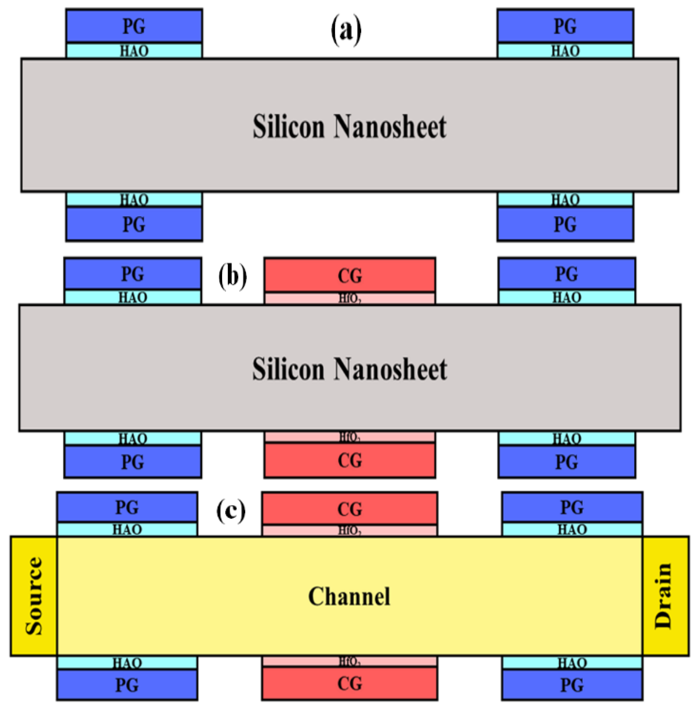
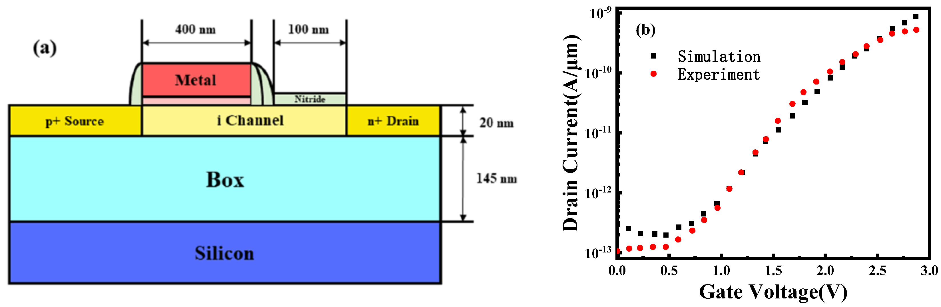
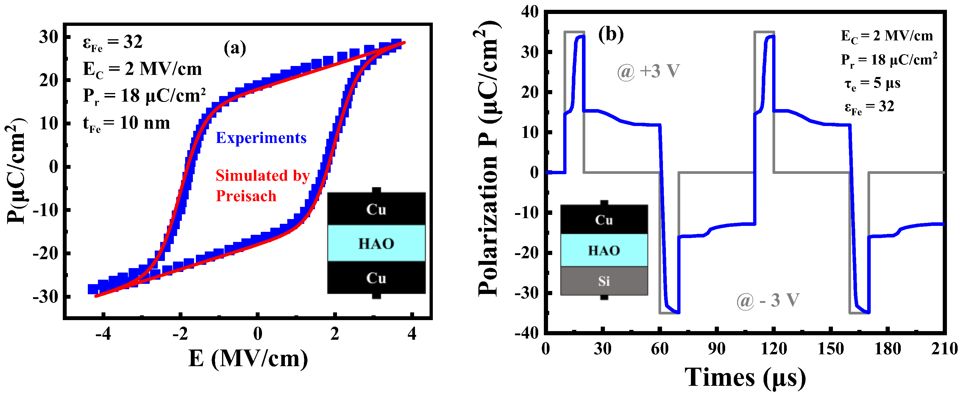
3.1. The Device Structure of Fe-ED NSTFET
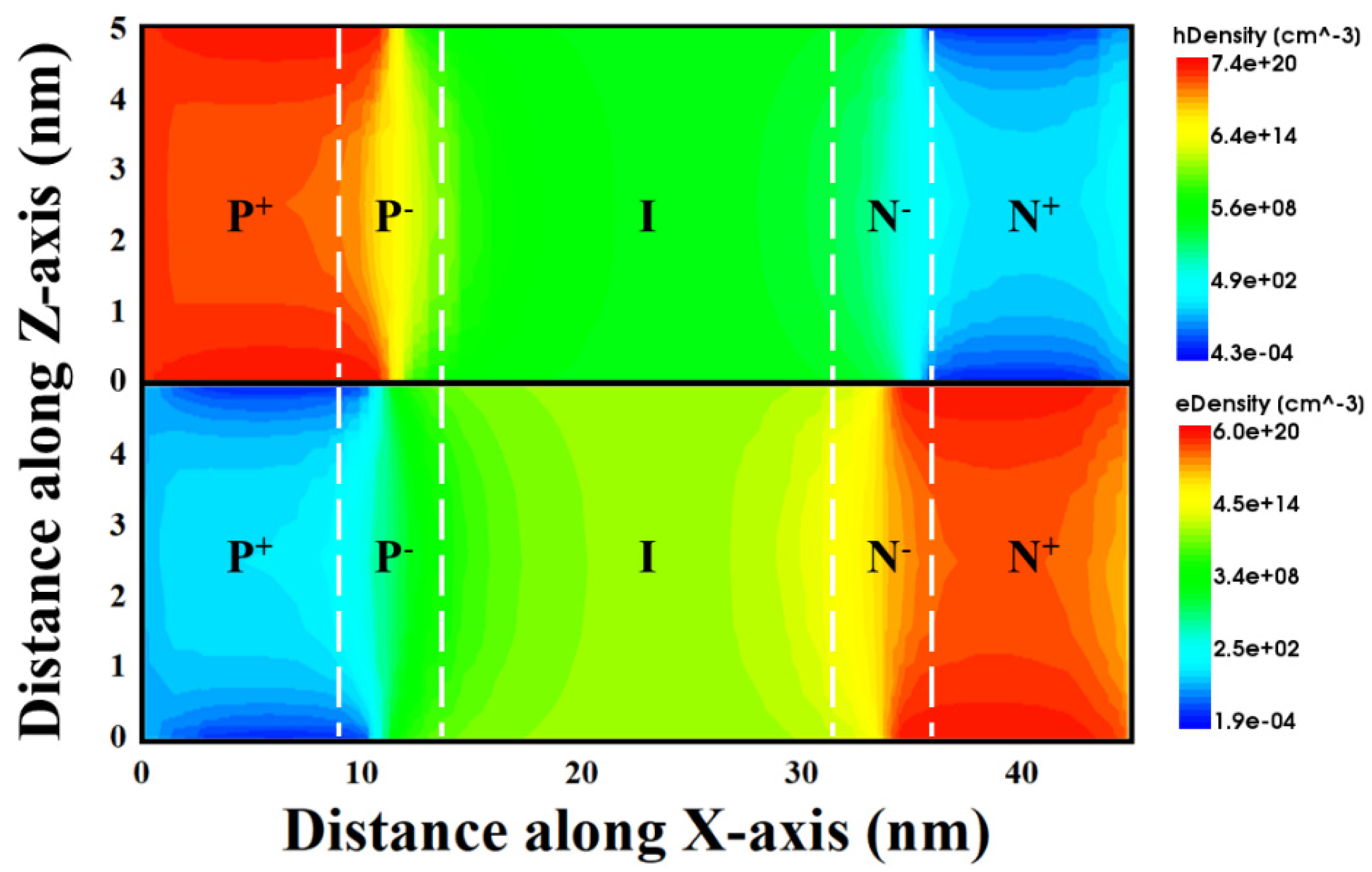
3.2. The Operating Mechanism of Fe-ED NSTFET
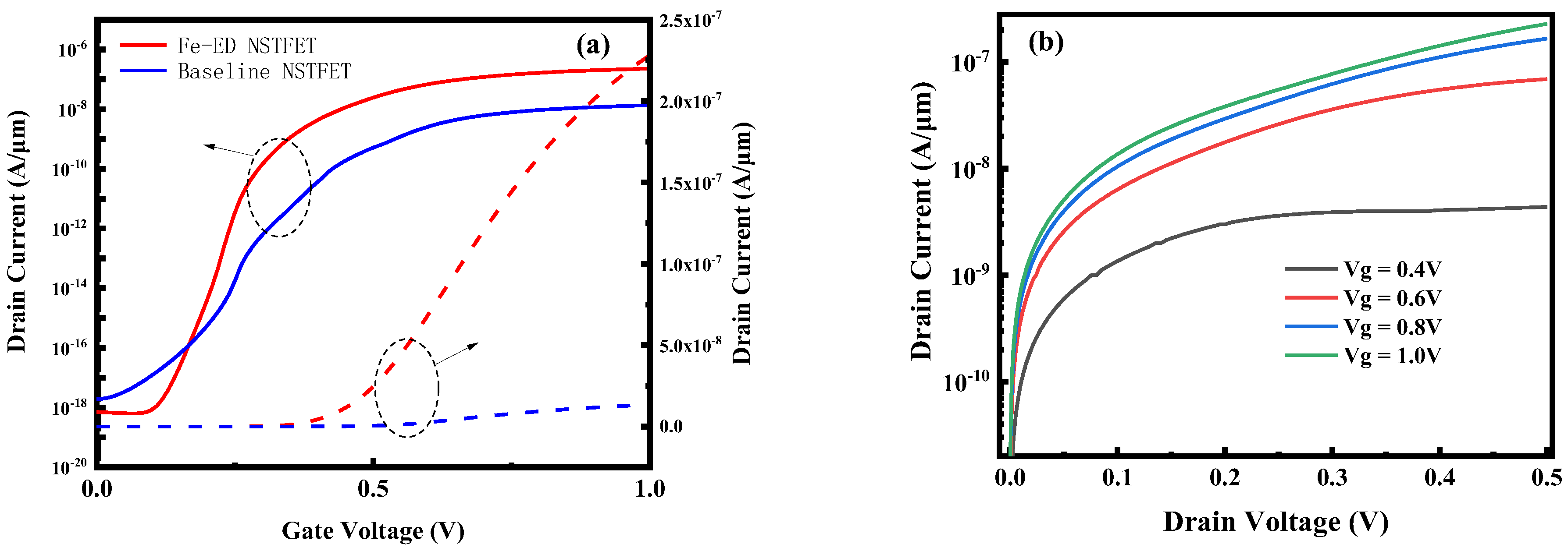
3.3. The Transfer and Output Characteristics Analysis
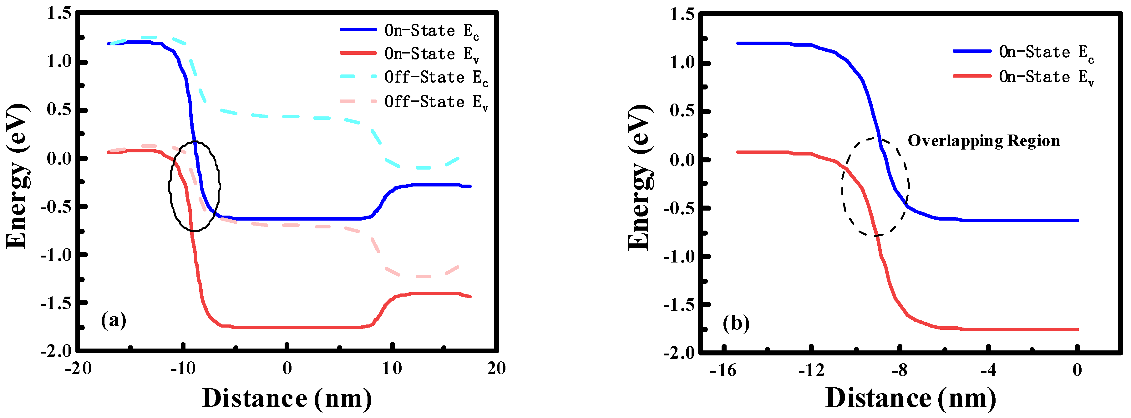
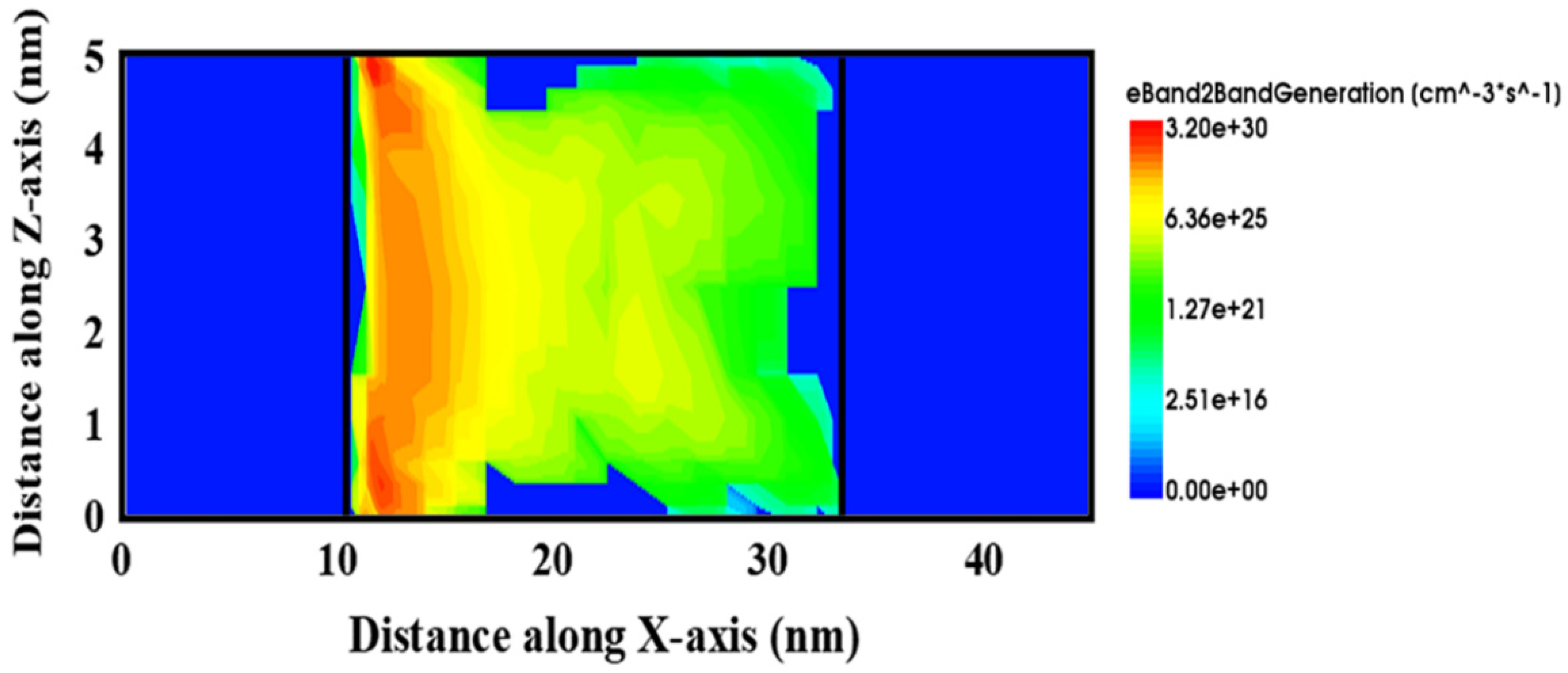
3.4. The Energy Band Analysis of Fe-ED NSTFET
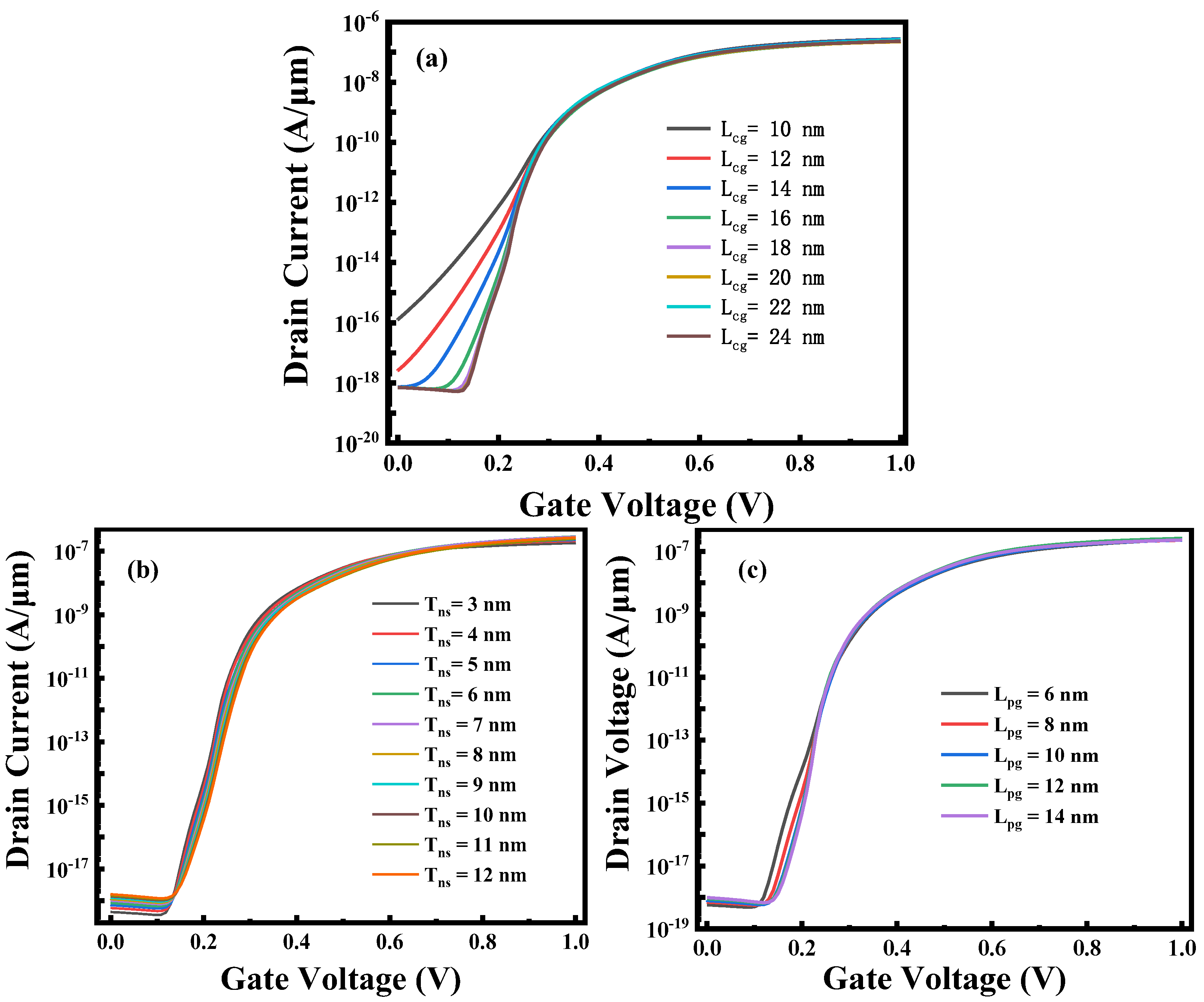
3.5. Scaling Capability of Fe-ED NSTFET
4. Conclusions
Author Contributions
Funding
Institutional Review Board Statement
Informed Consent Statement
Data Availability Statement
Conflicts of Interest
References
- Lee, Y.; Park, G.-H.; Choi, B.; Yoon, J.; Kim, H.-J.; Kim, D.H.; Kim, D.M.; Kang, M.-H.; Choi, S.-J. Design study of the gate-all-around silicon nanosheet MOSFETs. Semicond. Sci. Tech. 2020, 35, 03LT1. [Google Scholar] [CrossRef]
- Tayal, S.; Ajayan, J.; Joseph, L.; Tarunkumar, J.; Nirmal, D.; Jena, B.; Nandi, A.A. Comprehensive investigation of vertically stacked silicon nanosheet field effect transistors: An analog/rf perspective. Silicon 2022, 14, 3543–3550. [Google Scholar] [CrossRef]
- Kola, S.R.; Thoti, N. Characteristics of gate-all-around silicon nanowire and nanosheet MOSFETs with various spacers. In Proceedings of the 2020 International Conference on Simulation of Semiconductor Processes and Devices (SISPAD), Kobe, Japan, 23 September–6 October 2020. [Google Scholar]
- Okamoto, H.; Kumai, Y.; Sugiyama, Y.; Mitsuoka, T.; Nakanishi, K.; Ohta, T.; Nozaki, H.; Yamaguchi, S.; Shirai, S.; Nakano, H. Silicon nanosheets and their self-assembled regular stacking structure. J. Am. Chem. Soc. 2010, 132, 2710–2718. [Google Scholar] [CrossRef]
- Hou, Y.T.; Li, M.F.; Low, T.; Kwong, D.L. Metal gate work function engineering on gate leakage of MOSFETs. IEEE Trans. Electron Devices 2004, 51, 1783–1789. [Google Scholar] [CrossRef]
- Bhuwalka, K.K.; Schulze, J.; Eisele, I. Scaling the vertical tunnel FET with tunnel bandgap modulation and gate workfunction engineering. IEEE Trans. Electron Devices 2005, 52, 909–917. [Google Scholar] [CrossRef]
- Yu, B.; Wann, C.H.; Nowak, E.D.; Noda, K.; Hu, C. Short-channel effect improved by lateral channel-engineering in deep-submicronmeter MOSFET’s. IEEE Trans. Electron Devices 1997, 44, 627–634. [Google Scholar]
- Uchechukwu, M.A.; Srivastava, V.M. Channel length scaling pattern for cylindrical surrounding double-gate (CSDG) MOSFET. IEEE Access 2020, 8, 121204–121210. [Google Scholar] [CrossRef]
- Chander, S.; Baishya, S.; Sinha, S.; Kumar, S.; Singh, P.; Baral, K.; Tripathy, M.; Singh, A.; Jit, S. Two-dimensional analytical modeling for electrical characteristics of Ge/Si SOI-tunnel FinFETs. Superlattices Microstruct. 2019, 131, 30–39. [Google Scholar] [CrossRef]
- Tamersit, K.; Kouzou, A.; Bourouba, H.; Kennel, R.; Abdelrahem, M. Synergy of electrostatic and chemical doping to improve the performance of junctionless carbon nanotube tunneling field-effect transistors: Ultrascaling, energy-efficiency, and high switching performance. Nanomaterials 2022, 12, 462. [Google Scholar] [CrossRef]
- Khan, A.I.; Keshavarzi, A.; Datta, S. The future of ferroelectric field-effect transistor technology. Nat. Electron. 2020, 3, 588–597. [Google Scholar] [CrossRef]
- Chen, S.; Wang, S.; Liu, H.; Li, W.; Wang, Q.; Wang, X. Symmetric U-shaped gate tunnel field-effect transistor. IEEE Trans. Electron Devices 2017, 64, 1343–1349. [Google Scholar] [CrossRef]
- Li, W.; Liu, H.; Wang, S.; Chen, S. Reduced miller capacitance in U-shaped channel tunneling FET by introducing heterogeneous gate dielectric. IEEE Electron Device Lett. 2017, 38, 403–406. [Google Scholar] [CrossRef]
- Colinge, J.-P.; Lee, C.-W.; Afzalian, A.; Akhavan, N.D.; Yan, R.; Ferain, I.; Razavi, P.; O’neill, B.; Blake, A.; White, M. Nanowire transistors without junctions. Nat. Nanotechnol. 2010, 5, 225–229. [Google Scholar] [CrossRef] [PubMed]
- Ghosh, B.; Akram, M.W. Junctionless tunnel field effect transistor. IEEE Electron Device Lett. 2013, 34, 584–586. [Google Scholar] [CrossRef]
- Gundapaneni, S.; Ganguly, S.; Kottantharayil, A. Bulk planar junctionless transistor (BPJLT): An attractive device alternative for scaling. IEEE Electron Device Lett. 2011, 32, 261–263. [Google Scholar] [CrossRef]
- Cristoloveanu, S.; Lee, K.H.; Park, H.; Parihar, M.S. The concept of electrostatic doping and related devices. Solid-State Electron. 2019, 155, 32–43. [Google Scholar] [CrossRef]
- Heinzig, A.; Slesazeck, S.; Kreupl, F.; Mikolajick, T.; Weber, W.M. Reconfigurable silicon nanowire transistors. Nano Lett. 2012, 12, 119–124. [Google Scholar] [CrossRef] [PubMed]
- Bhattacharjee, A.; Saikiran, M.; Dutta, A.; Anand, B.; Dasgupta, S. Spacer engineering-based high-performance reconfigurable FET with low off current characteristics. IEEE Electron Device Lett. 2015, 36, 520–522. [Google Scholar] [CrossRef]
- Trommer, J.; Heinzig, A.; Slesazeck, S.; Mikolajick, T.; Weber, W.M. Elementary aspects for circuit implementation of reconfigurable nanowire transistors. IEEE Electron Device Lett. 2013, 35, 141–143. [Google Scholar] [CrossRef]
- Bae, J.-H.; Kim, H.; Kwon, D.; Lim, S.; Lee, S.-T.; Park, B.-G.; Lee, J.-H. Reconfigurable field-effect transistor as a synaptic device for XNOR binary neural network. IEEE Electron Device Lett. 2019, 40, 624–627. [Google Scholar] [CrossRef]
- Zhang, S.; Liu, Y.; Zhou, J.; Ma, M.; Gao, A.; Zheng, B.; Li, L.; Su, X.; Han, G.; Zhang, J. Low voltage operating 2D MoS2 ferroelectric memory transistor with Hf1−xZrxO2 gate structure. Nanoscale Res. Lett. 2020, 15, 1–9. [Google Scholar] [CrossRef] [PubMed]
- Liu, H.; Wang, C.; Han, G.; Li, J.; Peng, Y.; Liu, Y.; Wang, X.; Zhong, N.; Duan, C.; Wang, X. ZrO2 ferroelectric FET for non-volatile memory application. IEEE Electron Device Lett. 2019, 40, 1419–1422. [Google Scholar] [CrossRef]
- Zhou, Z.; Zhou, J.; Wang, X.; Wang, H.; Sun, C.; Han, K.; Kang, Y.; Zheng, Z.; Ni, H.; Gong, X. A Metal-Insulator-Semiconductor Non-Volatile Programmable Capacitor Based on a HfAlOx Ferroelectric Film. IEEE Electron Device Lett. 2020, 41, 1837–1840. [Google Scholar] [CrossRef]
- Peng, Y.; Xiao, W.; Han, G.; Liu, Y.; Liu, F.; Liu, C.; Zhou, Y.; Yang, N.; Zhong, N.; Duan, C. Memory behavior of an Al2O3 gate dielectric non-volatile field-effect transistor. IEEE Electron Device Lett. 2020, 41, 1340–1343. [Google Scholar] [CrossRef]
- Dünkel, S.; Trentzsch, M.; Richter, R.; Moll, P.; Fuchs, C.; Gehring, O.; Majer, M.; Wittek, S.; Müller, B.; Melde, T. A FeFET based super-low-power ultra-fast embedded NVM technology for 22nm FDSOI and beyond. In Proceedings of the 2017 IEEE International Electron Devices Meeting (IEDM), San Francisco, CA, USA, 2–6 December 2017. [Google Scholar]
- De Marchi, M.; Sacchetto, D.; Frache, S.; Zhang, J.; Gaillardon, P.-E.; Leblebici, Y.; De Micheli, G. Polarity control in double-gate, gate-all-around vertically stacked silicon nanowire FETs. In Proceedings of the 2012 International Electron Devices Meeting, San Francisco, CA, USA, 10–13 December 2012. [Google Scholar]
- Zhou, J.; Zhou, Z.; Wang, X.; Wang, H.; Sun, C.; Han, K.; Kang, Y.; Gong, X. Temperature Dependence of Ferroelectricity in Al-Doped HfO2 Featuring a High Pr of 23.7 μC/cm2. IEEE Trans. Electron Devices 2020, 67, 5633–5638. [Google Scholar] [CrossRef]
- Zhou, J.; Zhou, Z.; Wang, X.; Wang, H.; Sun, C.; Han, K.; Gong, X. Demonstration of ferroelectricity in Al-doped HfO2 with a low thermal budget of 500 °C. IEEE Electron Device Lett. 2020, 41, 1130–1133. [Google Scholar]
- Zhou, Z.; Jiao, L.; Zhou, J.; Zheng, Z.; Chen, Y.; Han, K.; Gong, X. Inversion-Type Ferroelectric Capacitive Memory and Its 1-Kbit Crossbar Array. IEEE Trans. Electron Devices 2023, 1–7. [Google Scholar] [CrossRef]
- Li, Y.; Lian, Y.; Yao, K.; Samudra, G.S. Evaluation and optimization of short channel ferroelectric MOSFET for low power circuit application with BSIM4 and Landau theory. Solid-State Electron. 2015, 114, 17–22. [Google Scholar] [CrossRef]
- Biswas, S.S.; Dan, C.L.; Royer, W.; Grabinski; Ionescu, A.M. TCAD simulation of SOI TFETs and calibration of non-local band-to-band tunneling model. Microelectron. Eng. 2012, 98, 334–337. [Google Scholar] [CrossRef]


| Parameters | Values |
|---|---|
| Remnant Polarization (Pr) | 18 µC/cm2 |
| Coercive Field (EC) | 2 MV/cm |
| Fe Relative Permittivity (εFe) | 32 |
| Thickness of Nanosheet (TNS) | 5 nm |
| Width of Nanosheet (WNS) | 50 nm |
| Length of Control Gate (LCG) | 14 nm |
| Length of Polarity Gate (LPG) | 8 nm |
| Length of Spacer (LSP) | 5 nm |
| Dielectric EOT (TDE) | 0.9 nm |
| Thickness of Fe Layer (TFe) | 5 nm |
| Work Function of Source/Drain (Φm) | 4.65 eV |
Disclaimer/Publisher’s Note: The statements, opinions and data contained in all publications are solely those of the individual author(s) and contributor(s) and not of MDPI and/or the editor(s). MDPI and/or the editor(s) disclaim responsibility for any injury to people or property resulting from any ideas, methods, instructions or products referred to in the content. |
© 2023 by the authors. Licensee MDPI, Basel, Switzerland. This article is an open access article distributed under the terms and conditions of the Creative Commons Attribution (CC BY) license (https://creativecommons.org/licenses/by/4.0/).
Share and Cite
Wang, D.; Liu, H.; Zhang, H.; Cai, M.; Lin, J. Modeling and Simulation Investigation of Ferroelectric-Based Electrostatic Doping for Tunnelling Field-Effect Transistor. Micromachines 2023, 14, 672. https://doi.org/10.3390/mi14030672
Wang D, Liu H, Zhang H, Cai M, Lin J. Modeling and Simulation Investigation of Ferroelectric-Based Electrostatic Doping for Tunnelling Field-Effect Transistor. Micromachines. 2023; 14(3):672. https://doi.org/10.3390/mi14030672
Chicago/Turabian StyleWang, Dong, Hongxia Liu, Hao Zhang, Ming Cai, and Jinfu Lin. 2023. "Modeling and Simulation Investigation of Ferroelectric-Based Electrostatic Doping for Tunnelling Field-Effect Transistor" Micromachines 14, no. 3: 672. https://doi.org/10.3390/mi14030672
APA StyleWang, D., Liu, H., Zhang, H., Cai, M., & Lin, J. (2023). Modeling and Simulation Investigation of Ferroelectric-Based Electrostatic Doping for Tunnelling Field-Effect Transistor. Micromachines, 14(3), 672. https://doi.org/10.3390/mi14030672