Article

Performance Improvement of In-Ga-Zn Oxide Thin-Film Transistors by Excimer Laser Annealing

1
Jihua Laboratory, Foshan 528200, China
2
School of Materials Science and Engineering, South China University of Technology, Guangzhou 510275, China
*
Author to whom correspondence should be addressed.
Micromachines 2024, 15(2), 225; https://doi.org/10.3390/mi15020225
Submission received: 28 December 2023 / Revised: 26 January 2024 / Accepted: 26 January 2024 / Published: 31 January 2024
(This article belongs to the Special Issue Future Prospects of Thin-Film Transistors and Their Applications)

Abstract

:
We applied excimer laser annealing (ELA) on indium-zinc oxide (IZO) and IZO/indium-gallium-zinc oxide (IGZO) heterojunction thin-film transistors (TFTs) to improve their electrical characteristics. The IZO and IZO/IGZO heterojunction thin films were prepared by the physical vapor deposition method without any other annealing process. The crystalline state and composition of the as-deposited film and the excimer-laser-annealed films were analyzed by X-ray diffraction and X-ray photoelectron spectroscopy. In order to further enhance the electrical performance of TFT, we constructed a dual-heterojunction TFT structure. The results showed that the field-effect mobility could be improved to 9.8 cm2/V·s. Surprisingly, the device also possessed good optical stability. The electron accumulation at the a-IZO/HfO, HfO/a-IGZO, and a-IGZO/gate insulator (GI) interfaces confirmed the a-IGZO-channel conduction. The dual-heterojunction TFT with IZO/HfO/a-IGZO-assisted ELA provides a guideline for overcoming the trade-off between high mobility (μ) and positive VTh control for stable enhancement mode operation with increased ID.

1. Introduction

In recent decades, amorphous metal-oxide semiconductor (AOS) thin-film transistors (TFTs) have attracted extensive attention. Among them, a-InGaZnO (a-IGZO) TFTs are highly favored because they exhibit higher carrier mobility than amorphous silicon TFTs, lower fabricated temperature and better large-area uniformity than those of poly-silicon TFTs, ultralow off-state current, and a steep subthreshold slope [1,2,3,4,5]. With the development of advanced applications, current-driven displays, and back-end-of-line devices, there is a need for AOS TFTs with much higher mobility. Generally speaking, thin films usually require annealing in oxygen or air, which may cause inconvenience in operation and even make it difficult to achieve large-scale annealing. By benefiting from the advantages of laser annealing, rapid annealing of large-area thin films can be conducted [6,7,8].
Improvements to AOS mobility usually include high-temperature annealing, induced crystallization, and the construction of heterojunctions [9,10,11,12,13,14]. According to the reported literature, their mechanisms have basically been clarified. Although the mobility-boosting mechanism in IGZO-based bilayer AOS TFTs has not been thoroughly clarified, it is normally associated with the heterojunction-induced quantum well and also interface defect suppression [15,16,17,18,19,20]. Considering the improvements to film quality by laser annealing and the influence of defects on double-layer AOS channels, we investigated the influence of laser annealing on bilayer AOS devices.
In this work, ELA was processed for postannealing of thin films to improve the electrical performance of devices. An a-IZO single-layer TFT, an a-IZO/a-IGZO heterojunction channel in a single-gate (SG) TFT, and an a-IZO/HfO/a-IGZO trilayer in a dual-gate (DG) TFT were controlled with a bottom-gate (BG) TFT. We attempted to analyze and compare the distinct dependences of the improvement mechanisms of laser annealing and assisted double-gate structures on mobility and stability and reveal the locations and formation mechanisms of carrier transport paths in the AOS heterojunction channel [21,22,23,24,25,26].

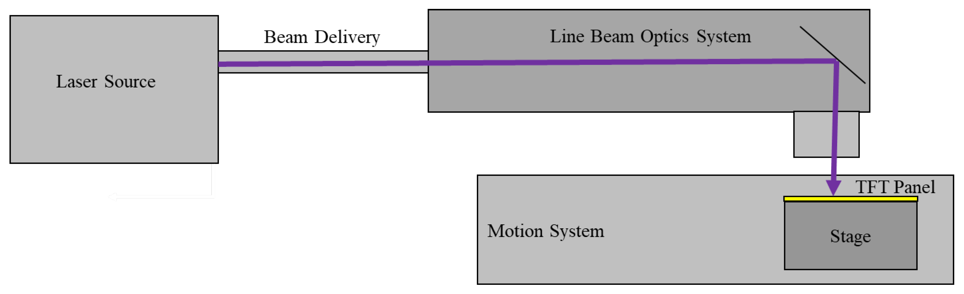
2. Materials and Methods

Film fabrication: A heavily doped p-Si wafer (gate electrode) with a thickness of 300 nm and a thermally grown SiO2 dielectric layer was employed as the substrate. First, the Si/SiO2 substrates were ultrasonically cleaned in acetone, alcohol, and deionized water sequentially and then blow-dried with nitrogen. Second, on the Si/SiO2 substrates, IZO (10 nm), HfOx (2 nm), and a-IGZO (10 nm) were sputtered in a mixed atmosphere of 10 sccm argon (Ar) and 2 sccm oxygen (O2) using direct sputtering of physical vapor deposition. ITO as a source-drain (S/D) electrode was prepared using radio-frequency sputtering. A relatively low power of 100 W was used to achieve a moderate deposition rate and also to suppress incidental bombardment damage to the underneath layer.
TFT fabrication: The AOS TFTs were fabricated in the bottom-gate structure on Si/SiO2 substrates. The active layers were made of a 10 nm thick a-IZO single-layer TFT, an a-IZO (10 nm)/a-IGZO (10 nm) dual-layer TFT, and an a-IZO (10 nm)/HfO (2 nm)/a-IGZO (10 nm) trilayer TFT. On the active layers, 100 nm thick sputtered InSnO (ITO) was patterned in DC mode using a mask, forming S/D electrodes with 20 μm channel length and 100 μm channel width.
Excimer laser annealing system: This consisted of a laser source of XeCl excimer laser; 308 nm wavelength; max. pulse energy of 1000 mJ; pulse duration of 24 ns ± 4 ns; max. laser repeat rate of 600 Hz; energy stability less than 1%; optics system laser line beam size of 750 (0–750 mm adjustable) × 0.25 mm; laser beam focus range within ±100 µm; max. energy density at substrate of 340 mJ/cm2; homogeneity of short axis less than 4%; homogeneity of long axis less than 1.8%; stage moving resolution of 0.1 μm; stage straightness less than 5 μm; and stage max. velocity of 400 mm/s (0–400 mm/s adjustable). A schematic diagram of the XeCl excimer laser annealing system is shown in Figure 1.
Figure 2a presents a picture to clearly exhibit the TFT structure of dual layers in this study. From this, we can see that the TFT device used Si as the substrate and acted as the gate electrode, with SiO2 acting as the gate dielectric layer. The subsequent heterojunction was grown on SiO2 by the PVD method to provide an active layer, forming a conductive channel for TFT. ITO was finally grown on the active layer as a source and drain electrode. Details of the sedimentary conditions can be found in the experimental section of the text. The schematic diagram of the annealing process of the XeCl excimer laser is shown in Figure 2. The linear laser beam annealed horizontally along the thin film via the stage, moving with the TFT substrate. Due to the controllable stage moving speed, fast TFT AOS surface annealing could be achieved, and the scanning range could also be controlled to achieve large-area surface annealing from the laser line beam size, which was 0–750 mm adjustable. The laser energy density can be adjusted to achieve the best TFT performance based on different film properties. Therefore, by adjusting the stage moving speed, laser line length, laser energy, laser repeat rate, etc., fast and large-scale annealing could be achieved.

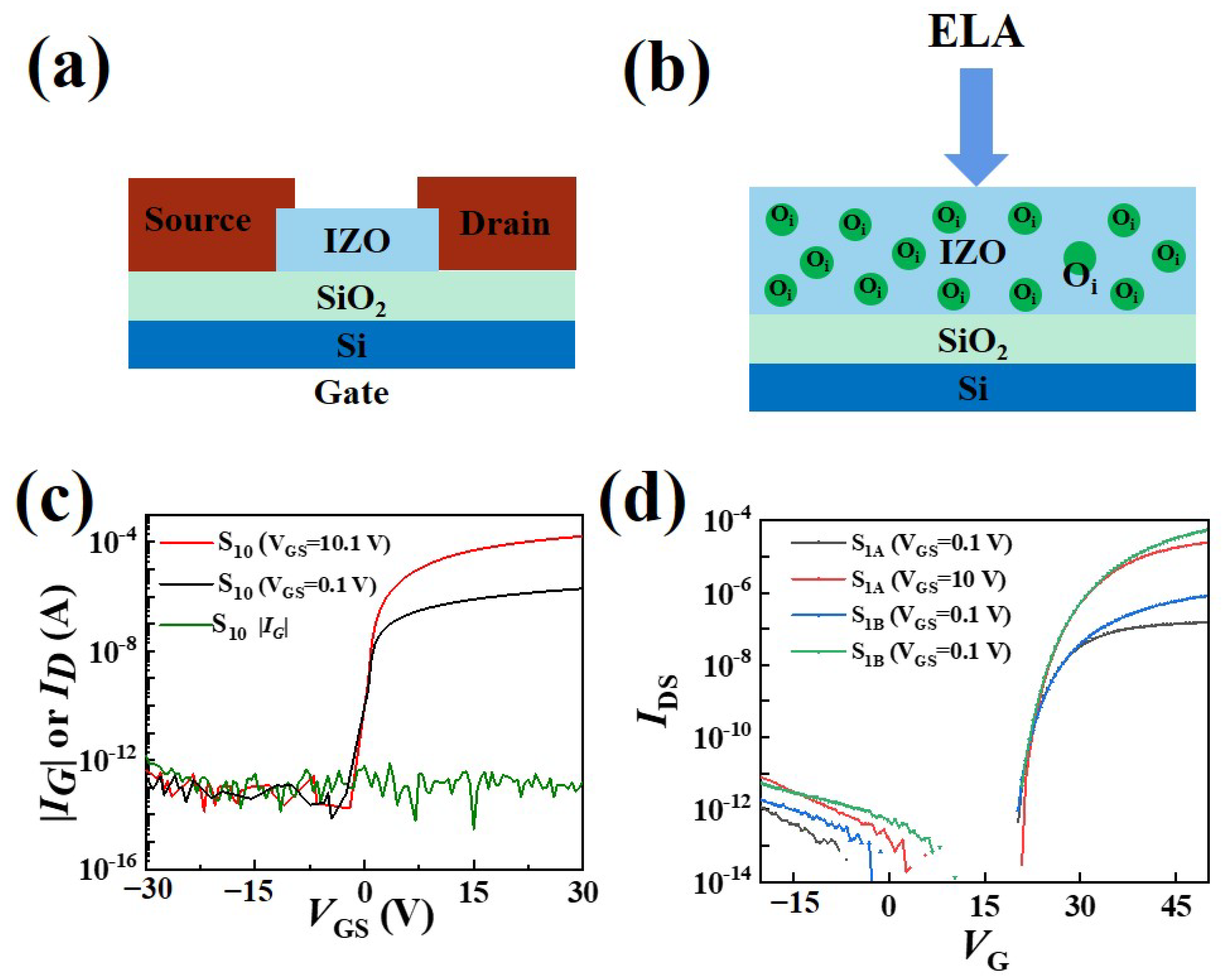
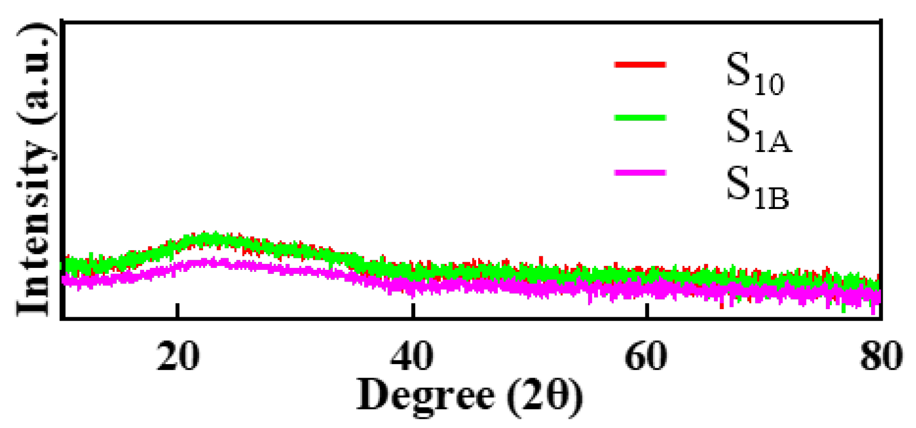
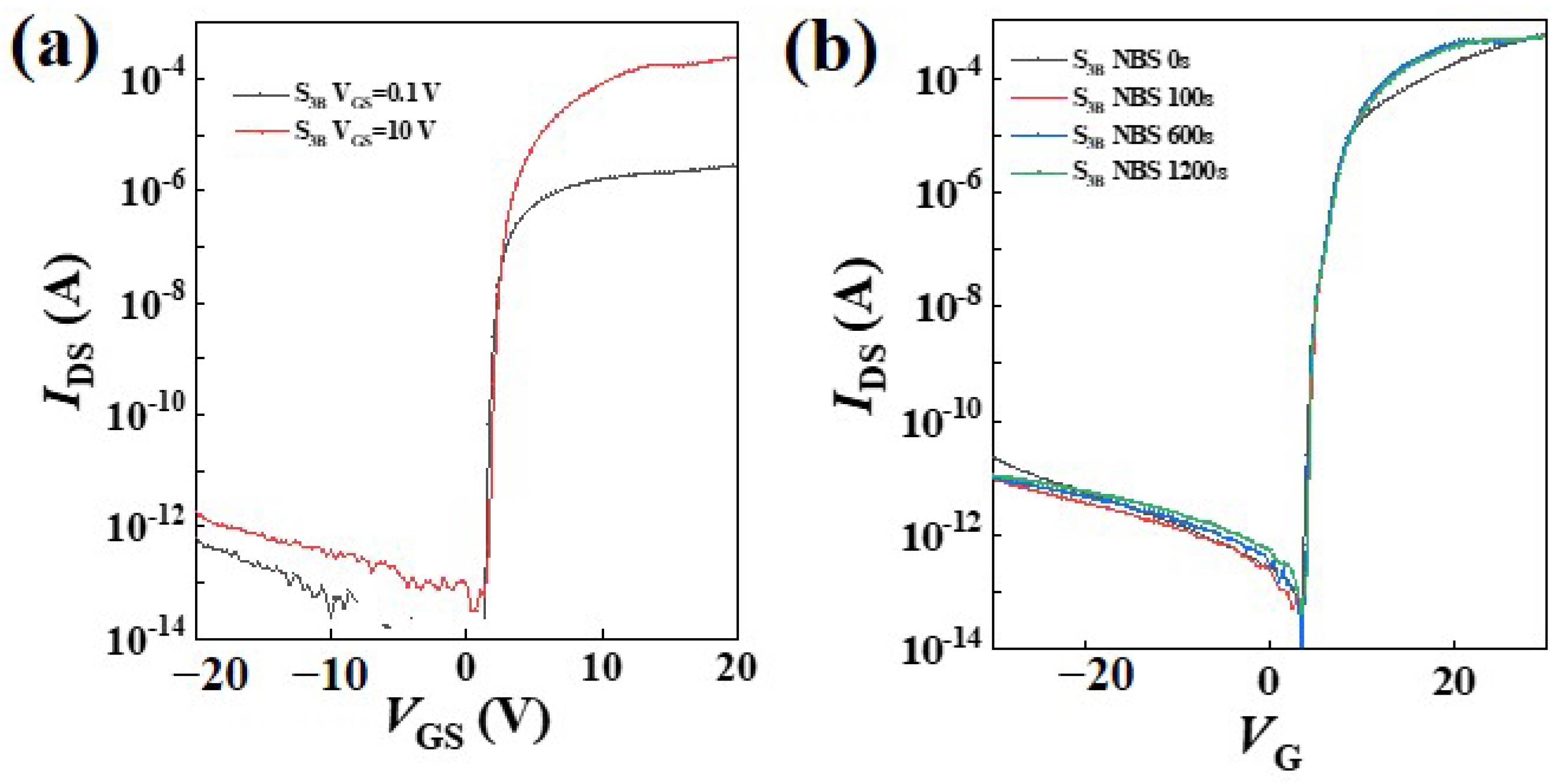
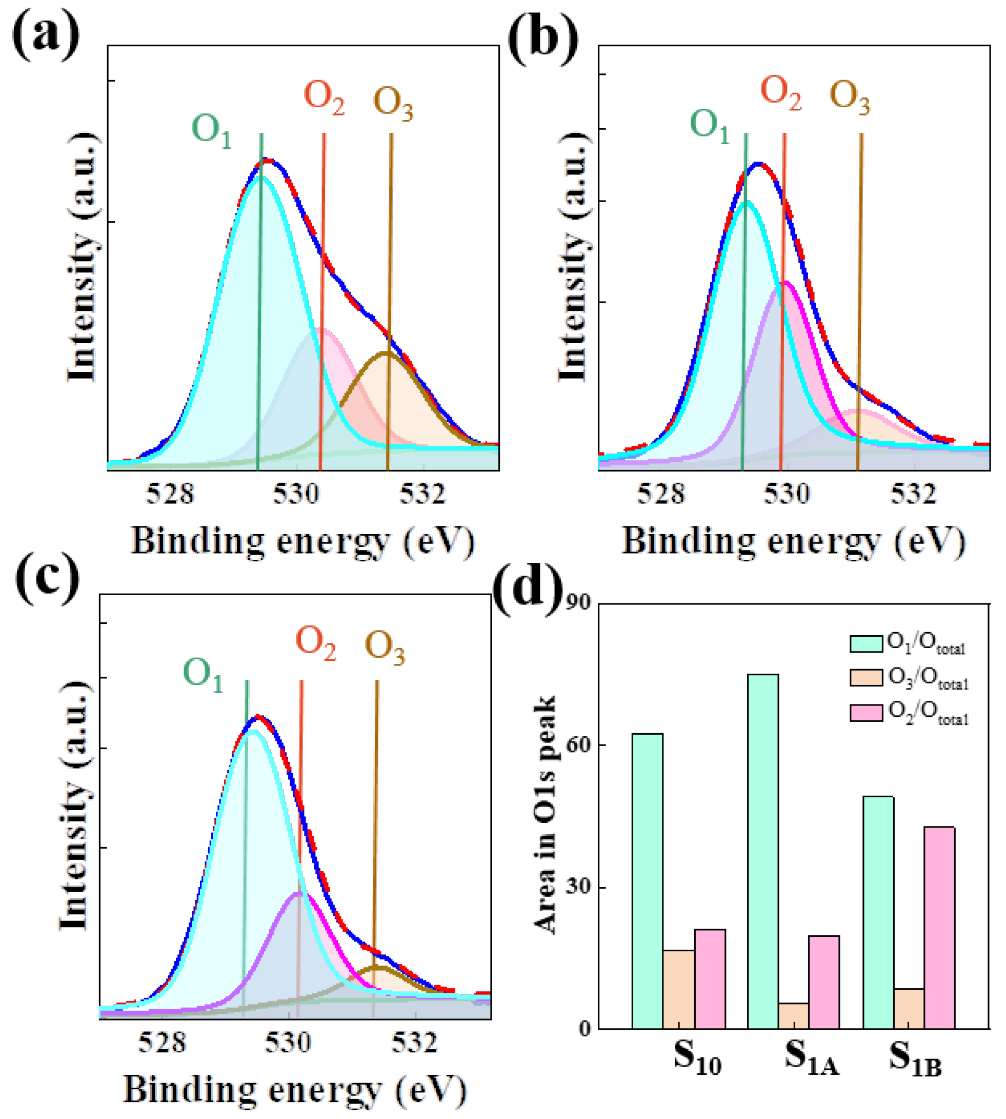
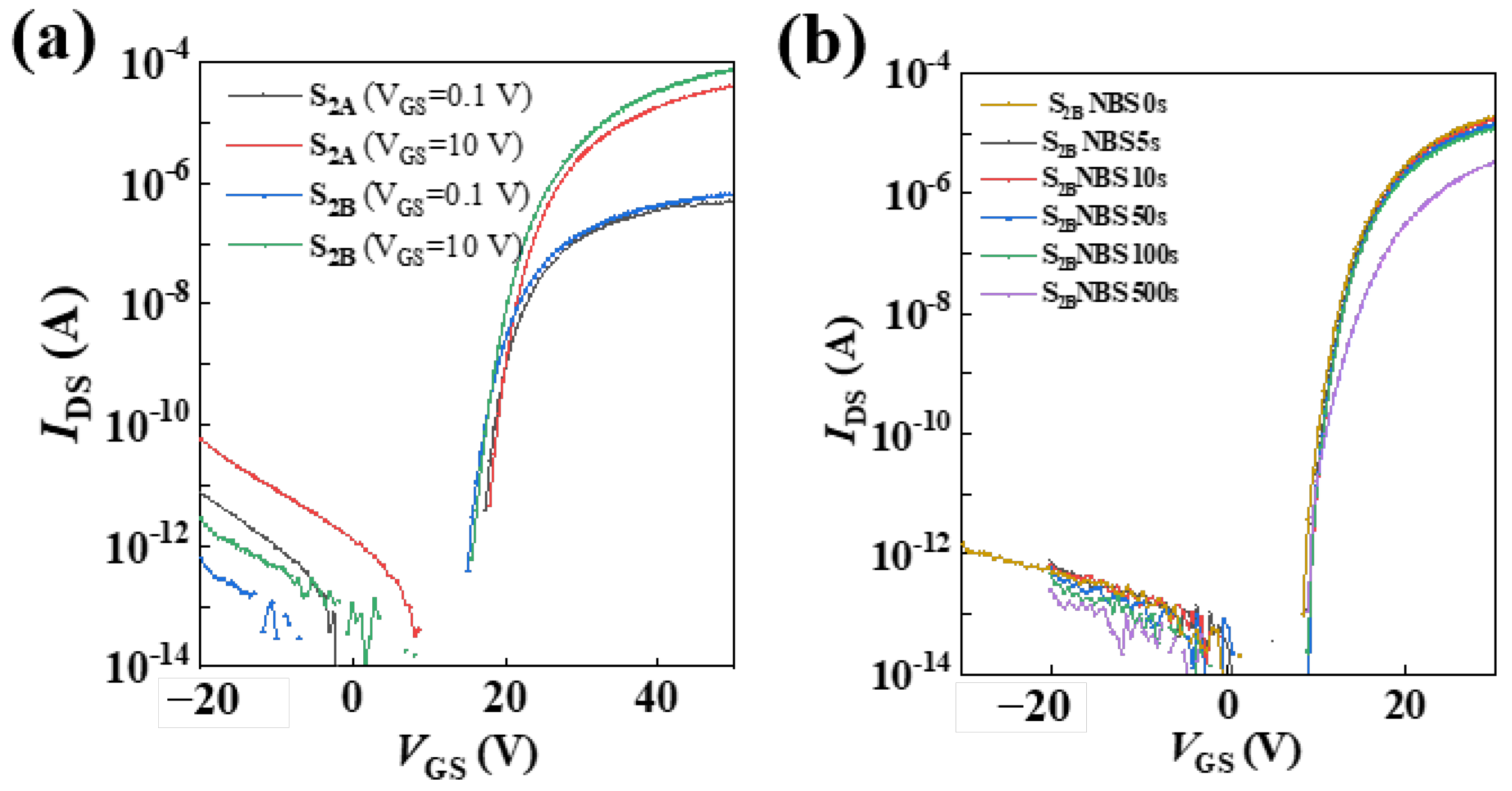
3. Results and Discussion

The TFT with single-active-layer IZO was successfully fabricated. Figure 3a shows a simplified diagram of the single-active-layer IZO TFT device, while Figure 3b shows the schematic diagram of the principle of laser annealing. Figure 3c shows the transfer (Ids-Vgs) curves of the TFT with single-active-layer IZO without ELA (labeled as S10). The thickness of the IZO layer was 10 nm. The TFT with single-active-layer IZO exhibited a mobility of 7.65 cm2/V·s, an acceptable threshold voltage (Vth, linear fitting based on IDS1/2-VGS curve) of 1.4 V, a subthreshold swing (SS, extracted from the linear portion of the log(IDS) versus VGS, SS = dVGS/dlogIDS) of 130 mV/decade, and a low off-current below 1 pA. Unfortunately, it exhibited an unclear pinch-off. As we all know, unclear pinch-off often slows down the switching speed of the TFT, which is not conducive to the implementation of fast response devices. Then, ELA was used for annealing treatment with laser energies of 200 and 250 mJ/cm2. Figure 3d shows the transfer curve of the IZO single-layer TFT after laser annealing at 200 and 250 mJ/cm2 laser energy (labeled as S1A and S1B, respectively). When ELA was applied, the TFT exhibited significant changes, such as field effect mobility of 0.69 and 3.45 cm2/Vs, Vth of 23.48 and 25.27 V, SS of 493 and 421 mV/decade at laser intensities of 200 and 250 mJ/cm2, respectively. Here, the calculation of mobility was based on the following formula:
I D S = W μ s a t C i 2 L ( V G V T ) 2
In the formula, IDS is the current between the source and the drain electrode; μsat is the carrier mobility in the saturated region; Ci is the capacitance; VG is the voltage applied between the source and the gate; VT is the threshold; and W and L are the width and length of conductive channels, respectively. Fortunately, the IZO single-layer TFT after ELA treatment exhibited a clear pinch-off. This phenomenon is attributed to the laser annealing process and may be due to a large number of M-O bond breaks during the ELA process, resulting in the generation of many interstitial oxygen vacancy defects in the IZO film that could capture electrons, ultimately leading to a significant positive threshold voltage of the device. This is similar to the pure oxygen annealing reported in the literature, where the oxygen partial pressure is reduced during the annealing process (such as by introducing argon gas), the gap oxygen defects are reduced, and the device Vth becomes negative accordingly [27,28,29,30].
We analyzed whether the crystalline state of the thin film changed before and after ELA using X-ray diffraction (XRD). The XRD spectrum in Figure 4 shows that there was no change in the crystalline state of the thin film before and after ELA, whether annealed at a laser intensity of 200 or 250 mJ/cm2. In a word, the thin films of the three devices were all amorphous. Then, we attempted to verify the rationality of the above conjecture about oxygen content by examining the O 1S content of the thin film.
Figure 5 shows the results of an X-ray photoelectron spectroscopy (XPS) analysis of the O1s peaks of the as-deposited a-IZO active layer without ELA processing and the a-IZO active layers with ELA processing at laser intensities of 200 and 250 mJ/cm2. As shown in Figure 5a, 5b for the a-IZO active layer without laser annealing and laser annealing at a laser intensity of 200 mJ/cm2, respectively, the ratio of the lattice oxygen peak (O1) to all O1s peaks increased from 62.75% to 74.9%, but the ratio of the hydroxide peak (O3) to all O1s peaks decreased from 16.5% to 5.3%. These results indicate that the oxygen vacancy concentration in the a-IZO thin film increased due to laser annealing, and this created an effect of an increase in electron concentration. Here, the oxygen vacancies played the role of doubly charged donors according to the relationship in the Kröger–Vink notation (Vox→Vo + 2e) [31,32,33,34,35]. As shown in Figure 5c, when the annealed laser intensity increased to 250 mJ/cm2 for the a-IZO active layer, the O1/Ototal value decreased to approximately 49.1%, while the O3/Ototal value decreased to approximately 8.3%. When the O1 peak becomes smaller and the oxygen vacancy peak (O2) peak becomes larger, the metal–oxygen bond is not restored properly, while the oxygen vacancies remain and the electron concentration increases. Therefore, the conductivity increases, and the saturation current should be appropriately increased. Therefore, our proposed fast laser annealing method will be effective for adjusting the performance of TFTs.
Next, we introduced the IZO/IGZO double layers as an active layer with ELA processed at laser intensities of 200 and 250 mJ/cm2 to improve the performance of the device (labeled as S2A and S2B, respectively). Also, we examined the Vth stability of the TFTs during the gate voltage stress.
It was found that the threshold voltage of the device decreased to 21.49 and 19.98 V when annealed at laser intensities of 200 and 250 mJ/cm2, respectively, as shown in Figure 6a. The mobility of the device did not show a significant improvement, with 2.04 at 200 mJ/cm2 and 1.91 at 250 mJ/cm2, respectively. As we all know, the IZO layer for high mobility has a lower resistance than the IGZO layer. The dual active layer of IZO/GIZO reduced the mobility of IZO, and both IZO and IGZO acted as conductive channels, resulting in a decrease in the overall mobility of the device [36,37,38]. Next, negative bias instability (NBS, VGS-stre = 30 V, and VDS = 10 V) under illumination at 250 lux of the heterojunction devices was tested. Surprisingly, the IZO/IGZO heterojunction device annealed by a 250 mJ/cm2 laser exhibited good optical stability, as shown in Figure 6b, which indicates that the Vth stability of the TFT with a double active layer was caused by the IGZO channel layer. At this point, IZO/IGZO heterojunction-assisted ELA did not have a significant effect on reducing the threshold of the device but was excellent at assisting negative bias illumination stability.
In order to improve the mobility and other performance metrics of the device without reducing the negative bias photostability, a dual-heterojunction structure (IZO/HFOx/IGZO) was constructed and annealed at a laser intensity of 250 mJ/cm2 (labeled as S3B). As shown in Figure 7a, the dual-heterojunction structure under 250 mJ/cm2 laser power showed a mobility of 9.8 cm2/V·s, Vth of 1.86 V, and SS of 97 mV/dec. Negative bias instability (NBS, VGS-stre = 30 V, and VDS = 10 V) under illumination at 250 lux was also tested. The dual-heterojunction TFT showed a Vth shift of less than 0.6 V, and these results were similar to those of the IZO/IGZO heterojunction TFT, as shown in Figure 7b. These results indicate that the Vth stability of the dual-heterojunction TFT was caused by the IGZO channel layer and had high mobility due to its dual-electron channels.
Table 1 was compiled to visually distinguish the impact of ELA and heterostructure construction on the performance of TFT devices.

4. Conclusions

This work created a-IZO, IZO/IGZO, and IZO/HfOx/IGZO TFTs by applying ELA for 200 and 250 mJ/cm2. To analyze the effect of ELA on a-IZO, and IZO/IGZO, IZO/Hfx/IGZO TFTs, XRD and XPS were carried out to analyze the properties of the films. In this study, the IZO/Hfx/IGZO TFTs to which a 250 mJ/cm2 laser was applied had an electron mobility of 9.8 cm2/V·s, an on-off-current ratio of 9.6 × 10⁸, and an SS value of 0.097 V/dec, which was a great improvement over the a-IZO TFT without the laser applied and the IZO/IGZO heterojunction devices processed by ELA. Therefore, we propose an effective method of ELA combined with a dual-heterojunction structure to improve both the mobility and stability of TFTs.

Author Contributions

Conceptualization, X.Z.; methodology, Y.L. (Yaping Li); formal analysis, Y.L. (Yanwei Li); investigation, X.X. and L.Y.; resources, X.Z.; data curation, Y.L. (Yaping Li); project administration, X.Z.; writing—original draft, Y.L. (Yaping Li); writing—review and editing, X.Z.; funding acquisition, X.Z. All authors have read and agreed to the published version of the manuscript.

Funding

This research was funded by the National Key Research and Development Program of China, grant number 2021YFB3602605.

Data Availability Statement

The data generated in the present study are available from the corresponding author upon reasonable request.

Conflicts of Interest

The authors declare no conflicts of interest.

References

  1. Yang, Y.-H.; Yang, S.S.; Chou, K.-S. Characteristic Enhancement of Solution-Processed In–Ga–Zn Oxide Thin-Film Transistors by Laser Annealing. IEEE Electron Device Lett. 2010, 31, 969–971. [Google Scholar] [CrossRef]
  2. Kim, J.-J.; Bak, J.-Y.; Lee, J.-H.; Kim, H.S.; Jang, N.-W.; Yun, Y.; Lee, W.-J. Characteristics of laser-annealed ZnO thin film transistors. Thin Solid Film. 2010, 518, 3022–3025. [Google Scholar] [CrossRef]
  3. Wang, P.; Yang, H.; Li, J.; Zhang, X.; Wang, L.; Xiao, J.; Zhao, B.; Zhang, S.; Lu, L. Synergistically Enhanced Performance and Reliability of Abrupt Metal-Oxide Heterojunction Transistor. Adv. Electron. Mater. 2022, 9, 2200807. [Google Scholar] [CrossRef]
  4. Lee, J.-Y.; Shan, F.; Kim, H.-S.; Kim, S.-J. Effect of Femtosecond Laser Postannealing on a-IGZO Thin-Film Transistors. IEEE Trans. Electron Devices 2021, 68, 3371–3378. [Google Scholar] [CrossRef]
  5. Kim, S.; Kim, C.J.; Park, J.C.; Song, I.; Kim, S.W.; Yin, H.; Lee, E.; Lee, J.C.; Park, Y. High Performance oxide thin Film Transistors with Dual Active Layers. In Proceedings of the 2008 IEEE International Electron Devices Meeting, San Francisco, CA, USA, 15–17 December 2008; pp. 1–4. [Google Scholar]
  6. Xu, M.; Peng, C.; Yuan, Y.; Li, X.; Zhang, J. Enhancing the Performance of Solution-Processed Thin-Film Transistors via Laser Scanning Annealing. ACS Appl. Electron. Mater. 2020, 2, 2970–2975. [Google Scholar] [CrossRef]
  7. Shan, F.; Sun, H.-Z.; Lee, J.-Y.; Pyo, S.; Kim, S.-J. Improved High-Performance Solution Processed In2O3 Thin Film Transistor Fabricated by Femtosecond Laser Pre-Annealing Process. IEEE Access 2021, 9, 44453–44462. [Google Scholar] [CrossRef]
  8. Jo, G.; Koh, J.-H. Laser annealing effects on Ga dopants for ZnO Thin films for transparent conducting oxide applications. Ceram. Int. 2019, 45, 6190–6197. [Google Scholar] [CrossRef]
  9. Huang, X.; Yu, G.; Wu, C. IGZO TFT-based circuit with tunable threshold voltage by laser annealing. Superlattices Microstruct. 2017, 111, 1172–1176. [Google Scholar] [CrossRef]
  10. Huang, H.-Y.; Wang, S.-J.; Wu, C.-H.; Lu, C.-Y. Improvement of Electrical Performance of InGaZnO/HfSiO TFTs with 248-nm Excimer Laser Annealing. Electron. Mater. Lett. 2014, 10, 899–902. [Google Scholar] [CrossRef]
  11. Huang, H.; Hu, H.; Zhu, J.; Guo, T. Inkjet-Printed In-Ga-Zn Oxide Thin-Film Transistors with Laser Spike Annealing. J. Electron. Mater. 2017, 46, 4497–4502. [Google Scholar] [CrossRef]
  12. Xu, M.; Hu, S.; Peng, C.; Jing, B.; Li, X.; Zhang, J. High Performance of Patterned Solution-Processed WZnSnO Thin Film Transistor Using Fiber-Coupler Semiconductor Laser Annealing. IEEE Trans. Electron Devices 2022, 69, 1858–1863. [Google Scholar] [CrossRef]
  13. Corsino, D.; Bermundo, J.P.; Fujii, M.N.; Ishikawa, Y.; Ikenoue, H.; Uraoka, Y. High Performance All-Solution Processed InZnO Thin-Film Transistors via Photo-Functionalization at Varying Fluence and Annealing Environment. SID Symp. Dig. Tech. Pap. 2022, 51, 1350–1353. [Google Scholar] [CrossRef]
  14. Nakata, M.; Takechi, K.; Azuma, K.; Tokumitsu, E.; Yamaguchi, H.; Kaneko, S. Improvement of InGaZnO4 Thin Film Transistors Characteristics Utilizing Excimer Laser Annealing. Appl. Phys. Express 2009, 2, 021102. [Google Scholar] [CrossRef]
  15. Li, Y.; Deng, C.; Huang, B.; Yang, S.; Xu, J.; Zhang, G.; Hu, S.; Wang, D.; Liu, B.; Zhong, J.; et al. High-Performance Solar-Blind UV Phototransistors Based on ZnO/Ga2O3 Heterojunction Channels. ACS Appl. Mater. Interfaces 2023, 15, 18372–18378. [Google Scholar] [CrossRef]
  16. Shi, J.W.; Wang, H.B.; Song, D.; Tian, H.K.; Geng, Y.H.; Yan, D.H. n-Channel, Ambipolar, and p-Channel Organic Heterojunction Transistors Fabricated with Various Film Morphologies. Adv. Funct. Mater. 2007, 17, 397–400. [Google Scholar] [CrossRef]
  17. Billah, M.-M.; Siddik, A.-B.; Kim, J.-B.; Yim, D.-K.; Choi, S.-Y.; Liu, J.; Severin, D.; Hanika, M.; Bender, M.; Jang, J. High-Performance Coplanar Dual-Channel a-InGaZnO/a-InZnO Semiconductor Thin-Film Transistors with High Field-Effect Mobility . Adv. Electron. Mater. 2021, 7, 2000896. [Google Scholar] [CrossRef]
  18. Khim, D.; Lin, Y.-H.; Nam, S.; Faber, H.; Tetzner, K.; Li, R.; Zhang, Q.; Li, J.; Zhang, X.; Anthopoulos, T.D. Modulation-Doped In2O3/ZnO Heterojunction Transistors Processed from Solution. Adv. Mater. 2017, 29, 1605837. [Google Scholar] [CrossRef] [PubMed]
  19. Lim, D.U.; Jo, S.B.; Kang, J.; Cho, J.H. Multi-State Heterojunction Transistors Based on Field-Effect Tunneling–Transport Transitions. Adv. Mater. 2021, 33, 2101243. [Google Scholar] [CrossRef] [PubMed]
  20. Faber, H.; Das, S.; Lin, Y.-H.; Pliatsikas, N.; Zhao, K.; Kehagias, T.; Dimitrakopulos, G.; Amassian, A.; Patsalas, P.A.; Anthopoulos, T.D. Heterojunction oxide thin-film transistors with unprecedented electron mobility grown from solution. Sci. Adv. 2017, 3, e160264. [Google Scholar] [CrossRef] [PubMed]
  21. Lee, J.-Y.; Tukhtaev, A.; Yoo, S.; Kim, Y.; Choi, S.; Ryu, H.G.; Jeong, Y.; Kim, S.-J. Improvement of Device Characteristics of Low Temperature IGZO Thin-film Transistors through Laser Post Annealing. Korean J. Met. Mater. 2022, 60, 557–563. [Google Scholar] [CrossRef]
  22. Huang, X.; Wu, C.; Lu, H.; Ren, F.; Chen, D.; Liu, Y.; Yu, G.; Zhang, R.; Zheng, Y.; Wang, Y. Large-Swing a-IGZO Inverter with a Depletion Load Induced by Laser Annealing. IEEE Electron Device Lett. 2014, 35, 1034–1036. [Google Scholar] [CrossRef]
  23. Fujii, M.; Ishikawa, Y.; Ishihara, R.; Cingel, J.; Mofrad, M.R.T.; Horita, M.; Uraoka, Y. Low temperature high-mobility InZnO thin-film transistors fabricated by excimer laser annealing. Appl. Phys. Lett. 2013, 102, 122107. [Google Scholar] [CrossRef]
  24. Lee, D.H.; Park, H.; Clevenger, M.; Kim, H.; Kim, C.; Liu, M.; Kim, G.; Song, H.W.; No, K.; Kim, S.Y.; et al. High-Performance Oxide-Based p–n Heterojunctions Integrating p-SnOx and n-InGaZnO. ACS Appl. Mater. Interfaces 2021, 13, 55676–55686. [Google Scholar] [CrossRef]
  25. Nakata, M.; Takechi, K.; Yamaguchi, S.; Tokumitsu, E.; Yamaguchi, H.; Kaneko, S. Effects of Excimer Laser Annealing on InGaZnO4 Thin-Film Transistors Having Different Active-Layer Thicknesses Compared with Those on Polycrystalline Silicon. Jpn. J. Appl. Phys. 2009, 48, 115505. [Google Scholar] [CrossRef]
  26. Wu, C.H.; Huang, H.Y.; Wang, S.J.; Chang, K.M. High-Mobility InGaZnO TFTs Using Atmospheric Pressure Plasma Jet Technique and 248-nm Excimer Laser Annealing. IEEE Electron Device Lett. 2014, 35, 1031–1033. [Google Scholar] [CrossRef]
  27. Nakata, M.; Takechi, K.; Eguchi, T.; Tokumitsu, E.; Yamaguchi, H.; Kaneko, S. Flexible High-Performance Amorphous InGaZnO4 Thin-Film Transistors Utilizing Excimer Laser Annealing. Jpn. J. Appl. Phys. 2009, 48, 081607. [Google Scholar] [CrossRef]
  28. Bermundo, J.P.S.; Ishikawa, Y.; Fujii, M.N.; Ikenoue, H.; Uraoka, Y. H and Au diffusion in high mobility a-InGaZnO thin-film transistors via low temperature KrF excimer laser annealing. Appl. Phys. Lett. 2017, 110, 133503. [Google Scholar] [CrossRef]
  29. Corsino, D.; Bermundo, J.; Kulchaisit, C.; Fujii, M.; Ishikawa, Y.; Ikenoue, H.; Uraoka, Y. High-Performance Fully Solution-Processed Oxide Thin-Film Transistors via Photo-Assisted Role Tuning of InZnO. ACS Appl. Electron. Mater. 2020, 2, 2398–2407. [Google Scholar] [CrossRef]
  30. Bae, E.-J.; Lee, J.Y.; Han, S.-Y.; Chang, C.-H.; Ryu, S. A Study on Indium Gallium Oxide Thin Film Transistors prepared by a Solution-based Deposition Method. Korean J. Chem. Eng. 2011, 49, 600–604. [Google Scholar] [CrossRef]
  31. Ebata, K.; Tomai, S.; Tsuruma, Y.; Iitsuka, T.; Matsuzaki, S.; Yano, K. High-Mobility Thin-Film Transistors with Polycrystalline In-Ga-O Channel Fabricated by DC Magnetron Sputtering. Appl. Phys. Express 2012, 5, 011102. [Google Scholar] [CrossRef]
  32. Rabbi, M.H.; Ali, A.; Park, C.; Jang, J. High Performance Amorphous In0.5Ga0.5O Thin-Film Transistor Embedded with Nanocrystalline In2O3 Dots for Flexible Display Application. Adv. Electron. Mater. 2023, 9, 2300169. [Google Scholar] [CrossRef]
  33. Huang, W.-L.; Hsu, M.-H.; Chang, S.-P.; Chang, S.-L.; Chiou, Y.-Z. Indium Gallium Oxide Thin Film Transistor for Two-Stage UV Sensor Application. ECS J. Solid State Sci. Technol. 2019, 8, Q3140–Q3143. [Google Scholar] [CrossRef]
  34. Park, S.; Cho, K.; Oh, H.; Kim, S. Electrical and mechanical characteristics of fully transparent IZO thin-film transistors on stress-relieving bendable substrates. Appl. Physis. Lett. 2016, 109, 143504. [Google Scholar] [CrossRef]
  35. Jeong, W.H.; Rim, Y.S.; Kim, D.L.; Kim, H.J. Improvement of electrical characteristics of solution-processed InZnO thin-film transistor by vacuum annealing and nitrogen pressure treatment at 200 °C. Jpn. J. Appl. Phys. 2015, 54, 126502. [Google Scholar] [CrossRef]
  36. Yao, J.; Xu, N.; Deng, S.; Chen, J.; She, J.; Shieh, H.-D.; Liu, P.; Huang, Y.-P. Electrical and photosensitive characteristics of a-IGZO TFTs related to oxygen vacancy. IEEE Trans. Electron Devices 2011, 58, 1121–1126. [Google Scholar]
  37. Guo, M.; Ou, H.; Xie, D.; Zhu, Q.; Wang, M.; Liang, L.; Liu, F.; Ning, C.; Cao, H.; Yuan, G.; et al. Critical Assessment of the High Carrier Mobility of Bilayer In2O3/IGZO Transistors and the Underlying Mechanisms. Adv. Electron. Mater. 2023, 9, 2201184. [Google Scholar] [CrossRef]
  38. Kamiya, T.; Nomura, K.; Hosono, H. Origins of High Mobility and Low Operation Voltage of Amorphous Oxide TFTs: Electronic Structure, Electron Transport, Defects and Doping. J. Disp. Technol. 2009, 5, 273–288. [Google Scholar] [CrossRef]
Figure 1. Schematic diagram of the XeCl excimer laser annealing system.
Micromachines 15 00225 g001
Figure 2. (a) Structure of a dual-layer TFT device. (b) Schematic diagram of the annealing process by XeCl excimer overlapping laser beams.
Micromachines 15 00225 g002
Figure 3. (a) Diagram of the TFT device. (b) Principle of ELA. (c) Transfer curve of the single IZO film (VDS = 0.1 and 10.1 V). (d) Transfer curve of the IZO film annealed at different laser intensities (S1A curves with 200 mJ/cm2 and S1B curves with 250 mJ/cm2).
Micromachines 15 00225 g003
Figure 4. XRD of samples S10, S1A, and S1B.
Micromachines 15 00225 g004
Figure 5. XPS spectra of O1s patterns of the a-IGZO active layers deposited by PVD. (a) As-deposited. (b) Laser annealed at a power of 200 mJ/cm2. (c) Laser annealed at a power of 250 mJ/cm2. (d) Area in the O1s peak of S10, S1A, and S1B.
Micromachines 15 00225 g005
Figure 6. (a) Transfer curve of the IZO/IGZO heterojunction TFT annealed at a laser power of 250 mJ/cm2. (b) Negative bias stability under illumination of the IZO/IGZO heterojunction TFT (250 lux white LED).
Micromachines 15 00225 g006
Figure 7. (a) Transfer curve of IZO/HfO/IGZO dual-heterojunction TFT annealed at a laser intensity of 250 mJ/cm2. (b) Negative bias stability under illumination of the IZO/HfO/IGZO heterojunction TFT (275 lux white LED).
Micromachines 15 00225 g007
Table 1. The electrical parameters of the TFTs with various active layers. The mobility (µ), SS, and Vth are summarized.
ChanelAnnealedVth (V)SS (mV/dec)μ (cm2/V·S)
S10As-deposited1.41287.65
S1AELA at 200 mJ/cm223.484930.69
S1BELA at 250 mJ/cm225.274213.45
S2AELA at 200 mJ/cm221.495902.04
S2BELA at 250 mJ/cm219.986671.91
S3BELA at 250 mJ/cm21.86979.8
S10: Sample of the single-layer IZO TFT without ELA; S1A: sample of the single-layer IZO TFT with ELA at laser intensity of 200 mJ/cm2; S1B: sample of the single-layer IZO TFT with ELA at laser intensity of 250 mJ/cm2; S2A: sample of the IZO/IGZO TFT with ELA at laser intensity of 200 mJ/cm2; S2B: sample of the IZO/IGZO TFT with ELA at laser intensity of 250 mJ/cm2; S3B: sample of the single-layer IZO/HfO/IGZO TFT with ELA at laser intensity of 200 mJ/cm2.
Disclaimer/Publisher’s Note: The statements, opinions and data contained in all publications are solely those of the individual author(s) and contributor(s) and not of MDPI and/or the editor(s). MDPI and/or the editor(s) disclaim responsibility for any injury to people or property resulting from any ideas, methods, instructions or products referred to in the content.

