Article

A High-Performance InGaAs Vertical Electron–Hole Bilayer Tunnel Field Effect Transistor with P+-Pocket and InAlAs-Block

School of Electronic and Information Engineering, Lanzhou Jiaotong University, Lanzhou 730070, China
*
Author to whom correspondence should be addressed.
Micromachines 2023, 14(11), 2049; https://doi.org/10.3390/mi14112049
Submission received: 14 October 2023 / Revised: 28 October 2023 / Accepted: 30 October 2023 / Published: 31 October 2023
(This article belongs to the Special Issue III–V Compound Semiconductors and Devices, 2nd Edition)

Abstract

:
To give consideration to both chip density and device performance, an In0.53Ga0.47As vertical electron–hole bilayer tunnel field effect transistor (EHBTFET) with a P+-pocket and an In0.52Al0.48As-block (VPB-EHBTFET) is introduced and systematically studied by TCAD simulation. The introduction of the P+-pocket can reduce the line tunneling distance, thereby enhancing the on-state current. This can also effectively address the challenge of forming a hole inversion layer in an undoped InGaAs channel during device fabrication. Moreover, the point tunneling can be significantly suppressed by the In0.52Al0.48As-block, resulting in a substantial decrease in the off-state current. By optimizing the width and doping concentration of the P+-pocket as well as the length and width of the In0.52Al0.48As-block, VPB-EHBTFET can obtain an off-state current of 1.83 × 10⁻¹⁹ A/μm, on-state current of 1.04 × 10⁻⁴ A/μm, and an average subthreshold swing of 5.5 mV/dec. Compared with traditional InGaAs vertical EHBTFET, the proposed VPB-EHBTFET has a three orders of magnitude decrease in the off-state current, about six times increase in the on-state current, 81.8% reduction in the average subthreshold swing, and stronger inhibitory ability on the drain-induced barrier-lowering effect (7.5 mV/V); these benefits enhance the practical application of EHBTFETs.

1. Introduction

Due to the emergence of the cloud, big data and real-time data transmission have become the main trends in the development of information technology, and they require integrated circuits to have ultra-low power dissipation. However, as the core of current integrated circuits, MOSFETs suffer from the increasing static power consumption with the decrease in feature size, inhibiting the development of integrated circuits. The decrease of subthreshold swing (SS) is an effective approach to deal with this issue. Limited by the injection mechanism of thermal emission, the SS of MOSFETs cannot be lower than 60 mV/dec; thus, there is an urgent need to develop steep SS (<60 mV/dec) devices to satisfy the cloud applications.
The tunnel field effect transistor (TFET) [1,2,3], as a steep SS device, has received widespread attention because of its CMOS process compatibility and low standby power consumption. However, the on-state current (Ion) of TFETs is too low for reasonable performance, which makes most research focus on overcoming this drawback. Therefore, TFETs with new structures or operation mechanisms have appeared in large numbers, such as two-dimensional material TFETs [4,5,6], negative capacitance TFETs [7,8,9], heterojunction TFETs [10,11,12], nanowire TFETs [13,14,15], line tunneling (L-tunneling) TFETs [16,17,18,19,20,21,22,23,24,25,26,27,28,29], etc. Comprehensive analysis shows that expanding the tunneling area based on the L-tunneling mechanism is a very effective approach to improving Ion. The electron–hole bilayer TFET (EHBTFET) [19,20,21,22,23,24,25,26,27,28,29] is a new type of L-tunneling TFET that was first proposed by Lattanzio [19] and has been developed in recent years because of its novel tunneling mechanism. Different from the L-tunneling TFETs with the L/U/T-type gate structure [16,17,18] that create the L-tunneling by overlapping the gate and heavily doped source region, EHBTFETs can generate the L-tunneling perpendicular to the channel in the electron–hole bilayer formed by the gate engineering or bias-induced method. So far, research has mainly focused on the transverse EHBTFETs, from which it has been found that the vertical L-tunneling not only boosts Ion but also leads to high off-state current (Ioff). To solve this issue, many methods, such as counterdoping in the gate underlap region [23], partial light doping in the source and drain regions [24], heterogate structure [25], and implantation of a dielectric barrier layer in the gate underlap region [26] have been adopted, and Ioff has been suppressed to a certain extent. However, it should be noted that the Ion of the transverse EHBTFETs is directly proportional to the gate overlap area, which means that the increase of Ion is at the expense of chip density. To simultaneously improve device performance and chip density, new EHBTFETs need to be investigated.
Vertical EHBTFETs [27,28,29] can improve Ion by expanding the tunneling area in the vertical direction without sacrificing the chip density, which attracts researchers’ attention. To further improve Ion, III-V materials are usually adopted in vertical EHBTFETs due to their smaller electron effective mass and band gap (Eg) [30], but which can also exacerbate the deterioration of Ioff. Our previous research [29] demonstrates that the impact of the point tunneling (P-tunneling) between the gate underlap region and the drain on the Ioff is significant, which cannot be effectively attenuated through the approaches used in transverse EHBTFETs. Although our proposed DGNP-EHBTFET in Reference [29] can solve this problem well, Ion can only be maintained without degradation and cannot be improved. To obtain better off- and on-state device performance, an improved vertical EHBTFET is proposed in this paper, namely, an In0.53Ga0.47As EHBTFET with a P+-pocket and an In0.52Al0.48As-block (VPB-EHBTFET). Since the line tunneling of EHBTFETs depends on the concentration of the electron–hole bilayer in the channel, the P+-pocket can be used to generate the hole layer in real operation. This is due to that for high-K/InGaAs interface, a large number of interface states near the valence band in InGaAs will inhibit the formation of the hole layer in the InGaAs channel without any acceptor doping. Although some methods, such as the use of Al2O3/HfO2 bilayer gate oxide [31], the postdeposition annealing process [32], and the gate-last process [33], can effectively reduce the interface trap density for the HfO2/InGaAs interface, P-type doping performed in the right-side channel may be the best method for creating the hole layer in real operation. More importantly, the P+-pocket can reduce the tunneling distance of the L-tunneling, which enhances the electron tunneling and achieves the goal of improving the on-state current. In0.52Al0.48As possesses greater Eg and carrier effective mass and matches the lattice of In0.53Ga0.47As. Due to its excellent material properties, placing In0.52Al0.48As in the gate underlap region near the drain can inhibit the point tunneling in this region. Moreover, it can also effectively avoid potential performance degradation caused by the lattice mismatch in the device fabrication. Heretofore, since investigations on suppressing off-state leakage and improving on-state performance for vertical EHBTFETs are relatively few, revealing the physical mechanism of the proposed VPB-EHBTFET is necessary, thereby providing theoretical guidance for device manufacturing.
The content of this paper focuses on the following aspects. Device structures and corresponding parameters, key manufacturing processes, and physical models for simulations are introduced in Section 2. Section 3 examines in detail the performance comparison between conventional and improved EHBTFETs and the effects of P+-pocket and InAlAs-block on the proposed VPB-EHBTFET. Finally, a concise summary of the current studies is provided in Section 4.

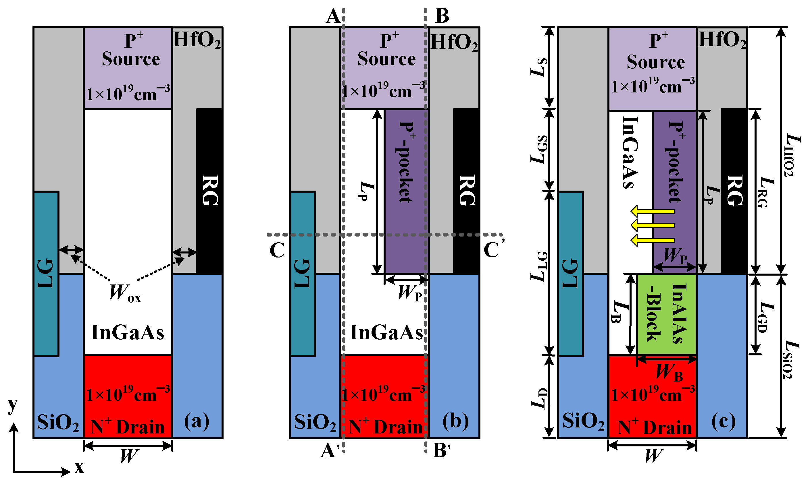
2. Device Structures and Simulation Methods

For comparison, we bring in two other EHBTFETs, namely, (1) a traditional vertical EHBTFET (V-EHBTFET) and (2) a vertical EHBTFET with a P+-pocket (VP-EHBTFET). Cross-sectional views and corresponding device parameters of the three EHBTFETs are given in Figure 1 and Table 1, respectively. It is found that EHBTFETs’ difference only exists in the channel. The bulk material of the three EHBTFETs is In0.53Ga0.47As, but there is an In0.52Al0.48As-block in the channel of VPB-EHBTFET compared with the other two devices. Moreover, only the channel near the right gate (RG) of VP-EHBTFET and VPB-EHBTFET possesses the P+-pocket with the doping concentration of 6 × 1019 cm−3. For these three EHBTFETs, since the L-tunneling occurs in the electron–hole bilayer of the gate overlap region (GO region) (see yellow arrows in Figure 1c), the appropriate carrier concentration is required in this region. According to the charge plasma concept [34], chromium (work-function = 4.5 eV) is employed as the left gate (LG) to induce a two-dimensional electron gas layer, and aurum (work-function = 5.3 eV) is adopted as RG to create a two-dimensional hole gas layer [35]. To induce a uniform carrier distribution, the width of bulk material is set to 10 nm. Furthermore, some key material parameters used in simulations refer to reference [10].
The proposed VPB-EHBTFET can be fabricated with the most advanced process technology currently available, in which the In0.53Ga0.47As epitaxial layer with the In0.52Al0.48As-block can be grown vertically on the InP substrate by molecular beam epitaxy technology, and the P+-pocket is created by ion implantation. Inductively coupled plasma etching is employed to etch dielectric and epitaxial layer materials, and the atom layer deposition technique can be adopted to deposit dielectrics and metal electrodes. The key process is the fabrication of the P+-pocket and the In0.52Al0.48As-block, which is closely related to the accurate control of doping depth and concentration in the ion implantation, as well as the precise design of the mask pattern.
All device simulations are performed using the Silvaco-Atlas 2-D numerical simulation platform. In simulations, the density gradient model is included to take into account the quantum confinement effect. Additionally, models included in references [10,29] are considered, such as the non-local band-to-band tunneling (BTBT) model, the Lombardi mobility model, the strained two-band zincblende model, etc. To compare under the same conditions, the influence of trap is not considered in the simulations.

3. Results and Discussion

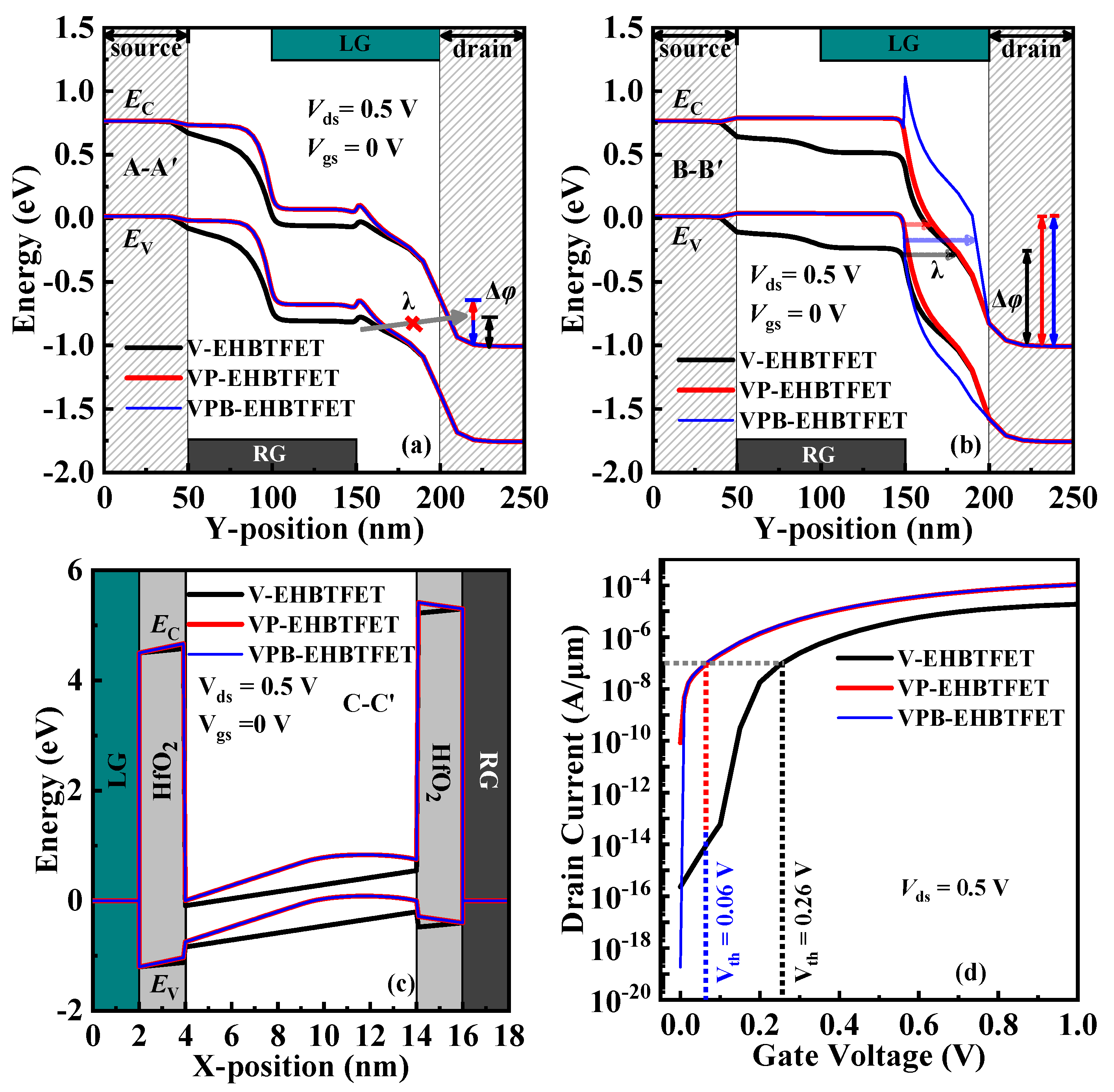
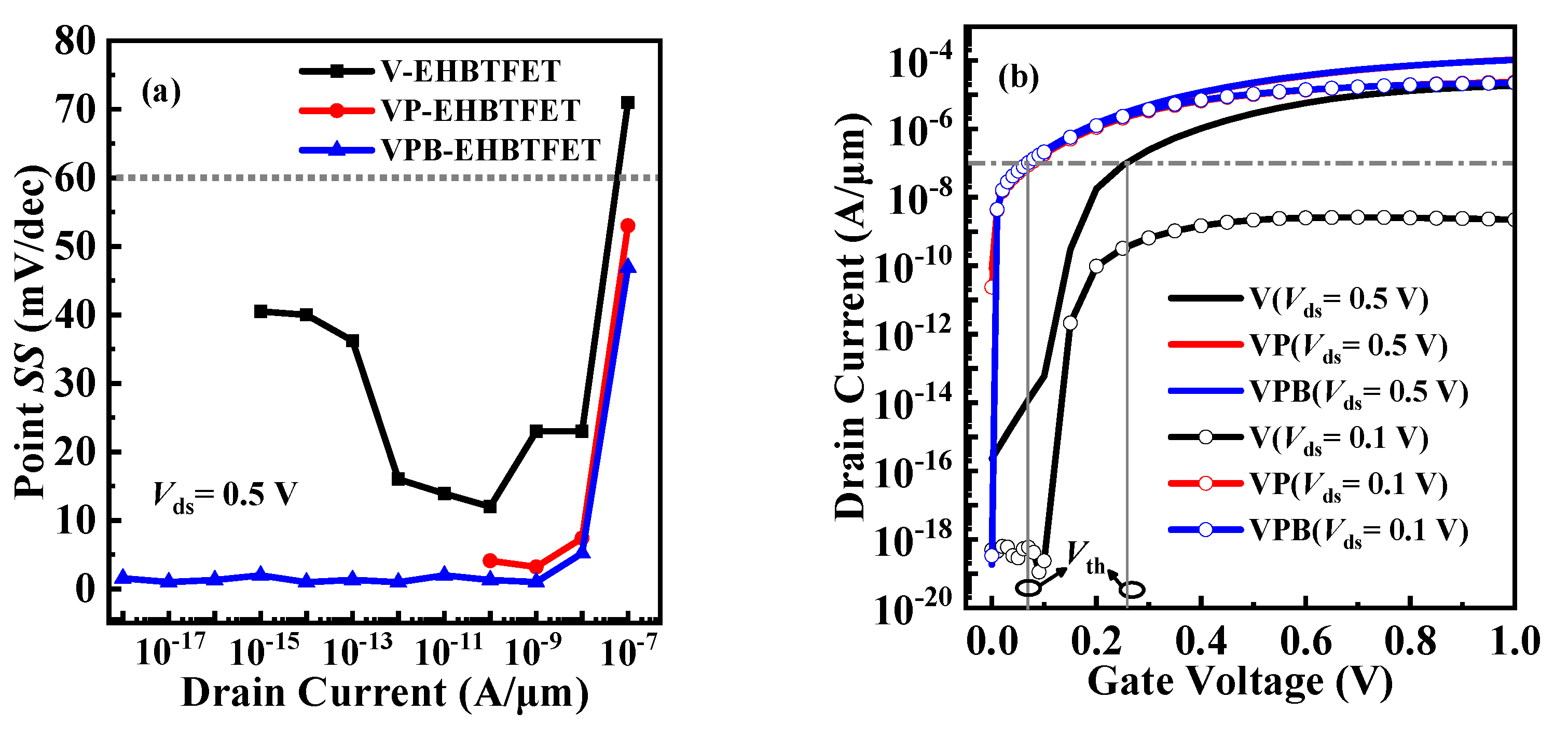
3.1. Performance Comparison between V-EHBTFET, VP-EHBTFET, and VPB-EHBTFET

Referring to our previous research on EHBTFETs [29], it is known that there are two tunneling mechanisms in this kind of device, namely, the P-tunneling and L-tunneling parallel to and perpendicular to the channel, respectively. The P-tunneling basically occurs in the gate underlap region near the source or drain (named GUS region or GUD region, respectively), while the L-tunneling occurs in the GO region. Both tunneling mechanisms are closely related to Ptun, which can be expressed as Equation (1) [29]:
P tun exp 4 λ 2 m * E g 3 / 2 3   |   e   |   ( E g + Δ φ ) = exp 4 2 m * E g 3 / 2 3   |   e   |   E
Two key factors affecting Ptun, the tunneling distance (λ) and the energy range used for tunneling (Δφ), can be extracted from the energy band. Therefore, to interpret the tunneling mechanism in detail, energy bands in the off-state [gate voltage (Vgs) = 0 V, drain voltage (Vds) = 0.5 V] for these three EHBTFETs are calculated along A-A′, B-B′, and C-C′ (gray dotted lines in Figure 1b), respectively, and plotted in Figure 2a–c, respectively.
As shown in Figure 2a, although Δφ appears in the GUD region, the P-tunneling in the left-side channel of the three EHBTFETs is suppressed due to the very long λ. It is observed from Figure 2b that the P-tunneling in the right-side channel also occurs in the GUD region. Since the introduction of a P+-pocket can enlarge Δφ and decrease λ, the P-tunneling in the off-state for VP-EHBTFET is stronger than that for V-EHBTFET, according to Equation (1). Although VPB-EHBTFET also possesses the P+-pocket like VP-EHBTFET, its P-tunneling can be better suppressed compared with the other two EHBTFETs. This is because there is an In0.52Al0.48As-block with wider Eg in the GUD region of VPB-EHBTFET, which significantly degrades the Ptun. Figure 2c shows the energy band profiles in the GO region, from which it is found that the L-tunneling does not take place in the off-state due to no Δφ. Based on the analyses in Figure 2a–c, it is concluded that in the off-state, the P-tunneling in the right-side channel is dominant, and the proposed VPB-EHBTFET has the weakest tunneling capacity. Ioff is an important parameter to test the off-state performance of devices, which can be extracted from the transfer characteristic curve (i.e., Ids-Vgs curve). To verify the above mechanism analysis, Ids-Vgs curves of these three EHBTFETs are computed and shown in Figure 2d. As observed from the figure, it results that Ioff of VPB-EHBTFET approaches as low as 1.83 × 10⁻¹⁹ A/μm. Compared with the Ioff of V-EHBTFET and VP-EHBTFET (2.29 × 10⁻¹⁶ A/μm and 8.37 × 10⁻¹¹ A/μm, respectively), that of VPB-EHBTFET is reduced by approximately three and eight orders of magnitude, respectively. It follows that VPB-EHBTFET has the best off-state performance, which is consistent with the tunneling mechanism analyzed above.
Ion, a key performance indicator in the on-state (Vgs = 1 V and Vds = 0.5 V in simulations), can also be extracted from Figure 2d. Ion of VPB-EHBTFET approaches 1.04 × 10⁻⁴ A/μm, which is basically the same as that of VP-EHBTFET but about 5.7 times higher than that of V-EHBTFET (1.84 × 10⁻⁵ A/μm). Here, we still explain their differences from the perspective of the energy band. Similarly, energy band profiles in the on-state for the three EHBTFETs are extracted and plotted in Figure 3.
From Figure 3a,b, the P-tunneling in the left-side channel occurs in the GUS region, which is different from that in the off-state, but that in the right-side channel still occurs in the GUD region. Based on the previous analysis, it can be known that the effect of the P+-pocket and the In0.52Al0.48As-block on the P-tunneling in the on-state is the same as that in the off-state. Combined with the P-tunneling in the left- and right-side channels, it can be inferred that the adoption of the P+-pocket is conducive to the enhancement of P-tunneling in the on-state. Furthermore, it is observed from Figure 3c that the energy bands in the GO region of VP-EHBTFET and VPB-EHBTFET bend upward due to the existence of the P+-pocket, which can reduce the λ of the L-tunneling and eventually enhance their L-tunneling. Since the L-tunneling occurs in the whole GO region (50 nm in length), while the P-tunneling region only exists within a range of a few nanometers near the gate, and the λ of L-tunneling is much smaller than that of P-tunneling, both of these cause the L-tunneling to dominate in the on-state. As a result, the tunneling ability of VP-EHBTFET and VPB-EHBTFET is basically the same in the on-state and stronger than that of V-EHBTFET, eventually resulting in better on-state performance in VP-EHBTFET and VPB-EHBTFET.
To better understand the tunneling mechanism of devices, it can be further investigated from the point of view of the non-local electron BTBT (e-BTBT) rate. According to the results of energy band analysis, only the off-state e-BTBT rate in the right-side channel and the on-state one in the GO region of V-EHBTFET, VP-EHBTFET, and VPB-EHBTFET are extracted and displayed in Figure 4a,b, respectively. It is found from Figure 4a that the peak values of the off-state e-BTBT rate for these three EHBTFETs occur in the GUD region and show the following trend: VP-EHBTFET >> V-EHBTFET >> VPB-EHBTFET, which directly reflects that the enhancement of the off-state P-tunneling by the P+-pocket can be suppressed significantly by the In0.52Al0.48As-block. The smaller the off-state e-BTBT rate of VPB-EHBTFET, the better its off-state performance. Figure 4b shows that the peak value of the on-state e-BTBT rate in the GO region of VP-EHBTFET and VPB-EHBTFET is the same, but it is one order of magnitude higher than that of V-EHBTFET. Thus, it can be confirmed again that the P+-pocket benefits improve the on-state L-tunneling, which makes the proposed VPB-EHBTFET have good on-state performance as VP-EHBTFET.
Furthermore, other important performance parameters, such as Ion/Ioff, subthreshold voltage (Vth), average subthreshold swing (SSavg), point subthreshold swing (point SS), and drain-induced barrier lowering (DIBL), are calculated based on the Ids-Vgs curves. Due to the high Ion and the minimum Ioff in the proposed VPB-EHBTFET, it obtains the maximum Ion/Ioff of 5.7 × 10¹⁴. Vth usually refers to the Vgs corresponding to the midpoint of the transition zone, where the drain current (Ids) changes sharply with the Vgs in the Ids-Vgs curve. Referring to previous publications [2,10], Vgs corresponding to Ids = 1 × 10⁻⁷ A/μm is taken as Vth in this paper. As shown in Figure 2d, the Vth of the proposed VPB-EHBTFET is as low as 0.06 V, which is the same as that of VP-EHBTFET. Moreover, the Vths of VPB-EHBTFET and VP-EHBTFET are less than that of V-EHBTFET (0.26 V). This is due to the introduction of P+-pocket reducing the λ of the L-tunneling, allowing VP- and VPB-EHBTFETs to be turned on at lower Vgs. SSavg is expressed as SSavg = (VthVoff)/(log IVth – log IVoff), where Voff is the Vgs at which the Ids begins to increase. In view of the minimum Ioff (i.e., IVoff) caused by the In0.52Al0.48As-block, SSavg of 5.5 mV/dec can be obtained in VPB-EHBTFET, which is reduced by 81.8% and 75.1% compared with that in V-EHBTFET and VP-EHBTFET (30.2 mV/dec and 22.1 mV/dec, respectively), respectively. Figure 5a shows the point SS values of the three EHBTFETs, where the point SS is calculated by dVgs/d(logIds). It is found that VPB-EHBTFET possesses steeper point SS at each Ids; in particular, when Ids < 10−8 A/μm, the point SS is around 1 mV/dec and basically remains unchanged, guaranteeing the steepest SSavg in VPB-EHBTFET. DIBL can be used to characterize the shift of Vth in devices, which is usually defined as ΔVthVds. To obtain the DIBL values of the three EHBTFETs, the Ids-Vgs curves are calculated at Vds = 0.1 V and 0.5 V, respectively, and plotted in Figure 5b. Since Vths of the proposed VPB-EHBTFET and VP-EHBTFET change negligibly under different Vdss, a low DIBL value of 7.5 mV/V can be achieved in both EHBTFETs. This is because the existence of the P+-pocket enhances the built-in electric field in the GO region, thereby reducing the influence of the applied electric field on the L-tunneling. However, the DIBL value cannot be calculated for V-EHBTFET because this device is still turned off at Vds = 0.1 V. Thus, it can be seen that the adoption of the P+-pocket can effectively suppress the DIBL effect. For a clear comparison, the parameters discussed above for the three EHBTFETs are summarized in Table 2.

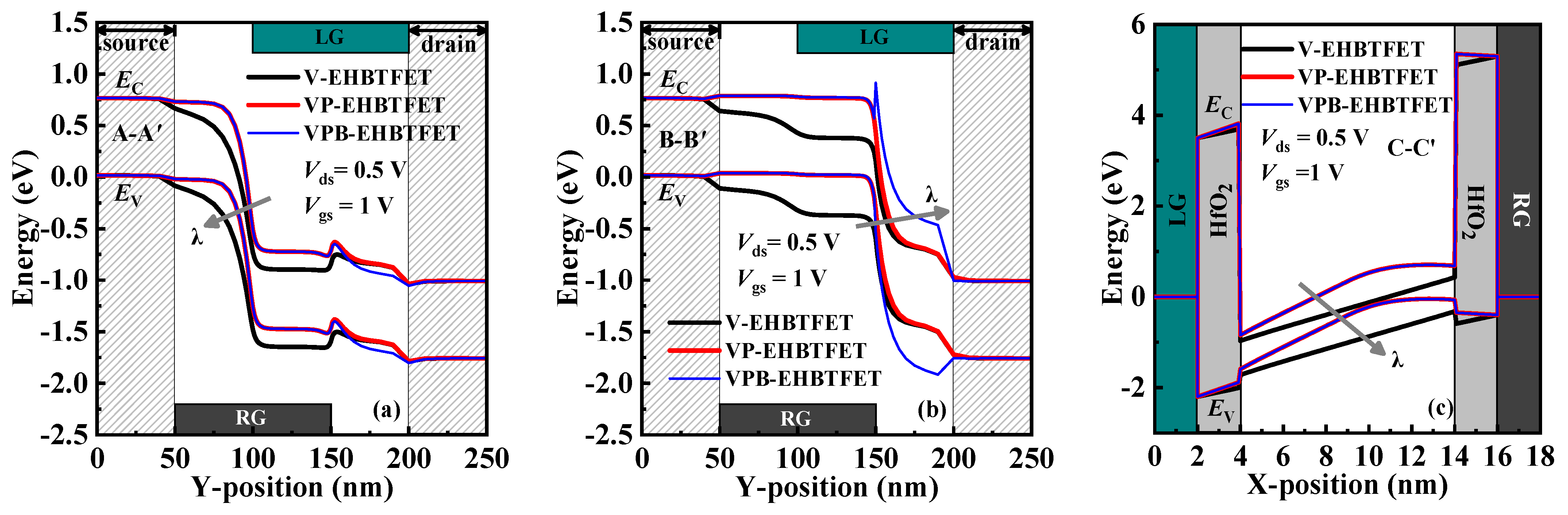
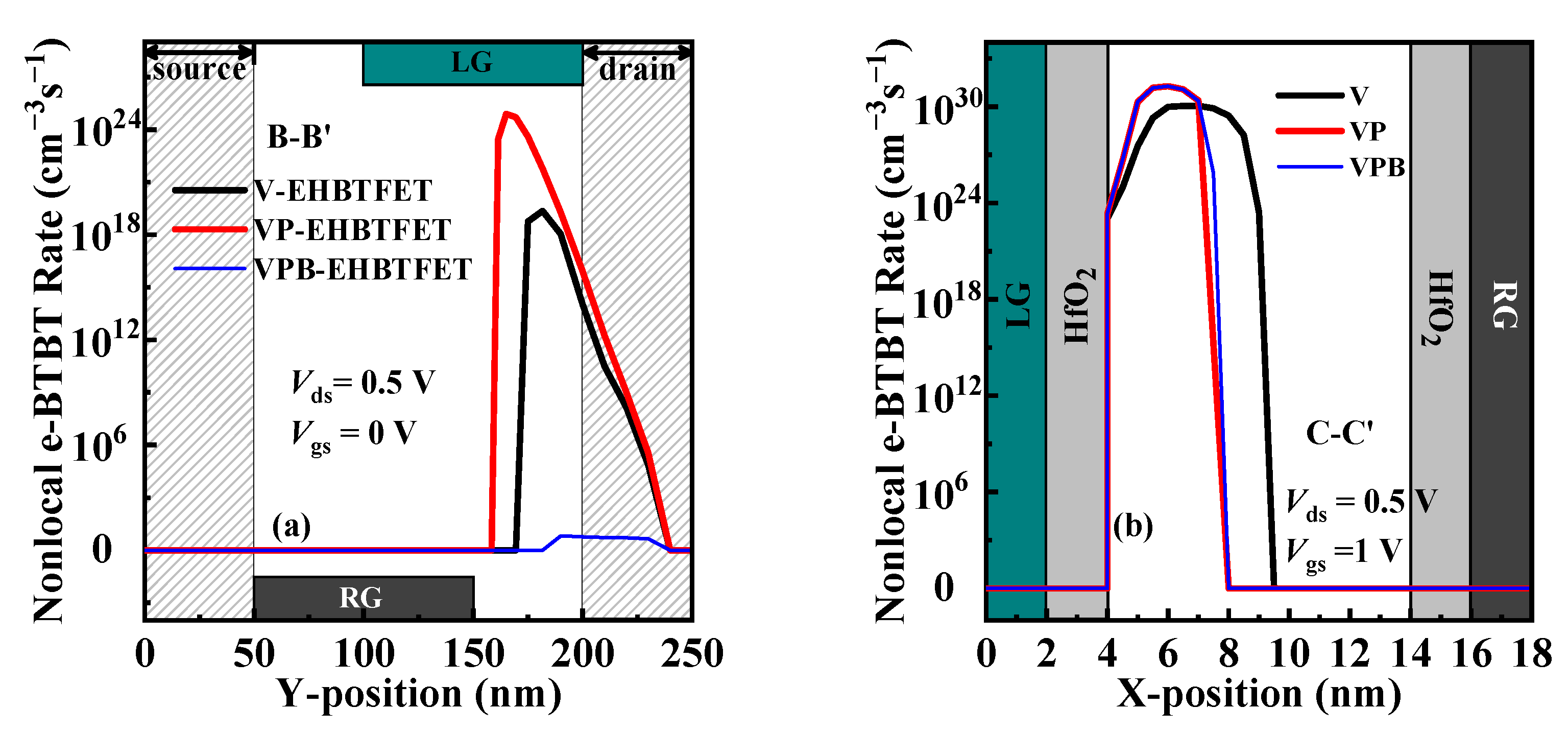
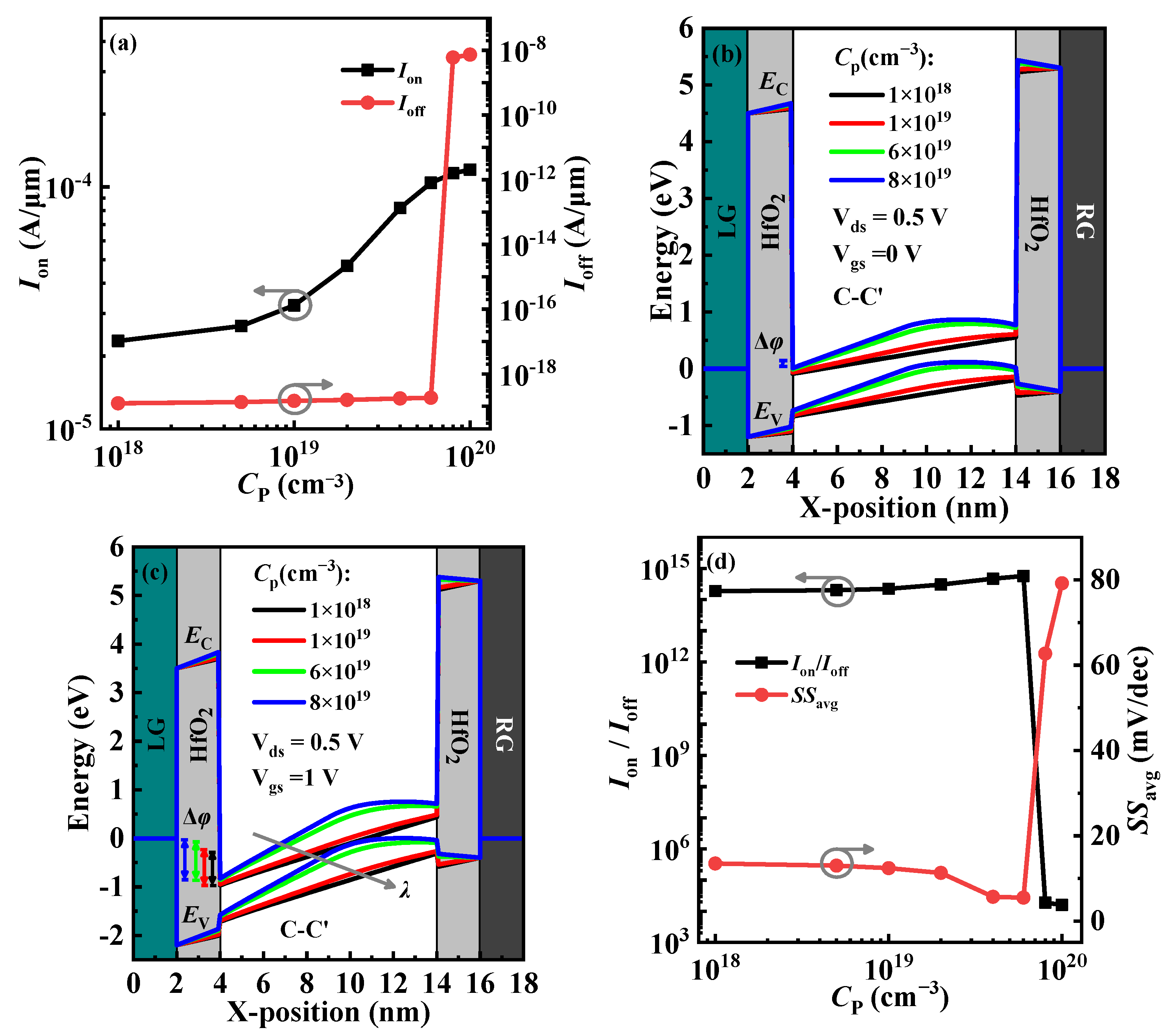
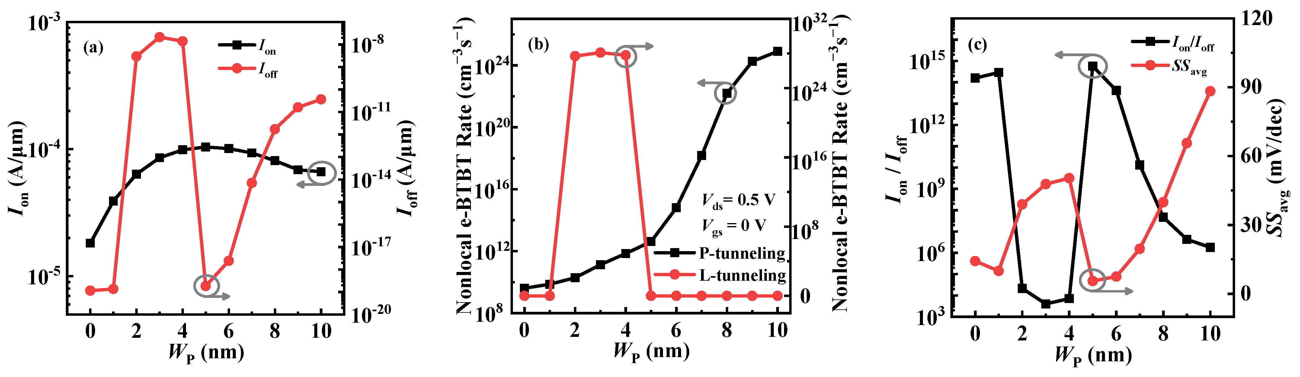
3.2. Effect of P+-Pocket on VPB-EHBTFET

Here, doping concentration and doping width (CP and WP) in the P+-pocket of the proposed VPB-EHBTFET are investigated for the optimization of device performance. Figure 6a shows Ion and Ioff values under different CPs. It is found from the figure that Ioff is very low and remains the same order of magnitude when CP < 8 × 1019 cm−3, but it increases sharply with the further increase in CP. Ion increases with CP. Both of these trends can be explained by the energy band profiles. Based on the conclusion of device performance comparison between conventional and improved EHBTFETs, it is known that their Ioff and Ion depend on the off-state P-tunneling in the GUD region of the right-side channel and the on-state L-tunneling in the GO region, respectively. Therefore, the off-state energy bands of the P-tunneling in the right-side channel under different CPs are calculated first, but results demonstrate that the effect of the change of CP on the P-tunneling is negligible. This is because the existence of the In0.52Al0.48As-block makes the λ of the P-tunneling possess basically identical lengths (about 50 nm) under different CPs, thereby preventing the tunneling of electrons in this region. Then, the off-state energy bands of the L-tunneling in the GO region under different CPs are also calculated and plotted in Figure 6b. With the increase in CP, the energy band gradually bends upward, and a Δφ can be generated when CP > 6 × 1019 cm−3. The existence of Δφ provides a condition for the off-state L-tunneling, which results in a rapid increase in Ioff. Moreover, for the interpretation of the change trend of Ion, the on-state energy bands of the L-tunneling in the GO region are examined and shown in Figure 6c. With the increase in CP, λ decreases and Δφ increases, so that Ion takes on a monotonically increasing trend according to Equation (1). Figure 6d shows SSavg and Ion/Ioff in VPB-EHBTFET with different CPs. With the increase in CP, SSavg decreases slowly first and then increases rapidly, but Ion/Ioff has the opposite change trend compared with SSavg. When CP = 6 × 1019 cm−3, SSavg and Ion/Ioff can approach the minimum and maximum values, respectively. By compromising performance parameters, it results that 6 × 1019 cm−3 is the optimal CP.
Further, the effect of doping width WP on the device performance is investigated. Figure 7a shows Ioff and Ion values under different WPs. With the increase in WP, Ioff increases first, then decreases, and finally increases again. To interpret this trend, we extract the e-BTBT rates that can reflect the tunneling ability of the P-tunneling and L-tunneling in the off-state and plot them in Figure 7b. It is observed from the figure that the off-state e-BTBT rates of the P-tunneling and L-tunneling are very low when WP ≤ 1 nm, which indicates that both kinds of tunneling are suppressed in this condition, so a very small Ioff can be obtained. When 1 nm < WP < 5 nm, the off-state L-tunneling is turned on and dominates, which makes Ioff have a sharp increase. This is due to the fact that the λ of the L-tunneling reduces with the increase in WP. With the further increase in WP, the decrease in electrons in the left side of the GO region lifts the energy band in this region; thus, the Δφ of the L-tunneling starts to reduce at WP = 4 nm and disappears at WP = 5 nm, thereby resulting in a decrease in Ioff. When WP ≥ 5 nm, the L-tunneling is turned off, and the P-tunneling is dominant, leading to Ioff increasing with WP again. This is because, with the increase in WP, the P-tunneling junction in the left-side channel becomes steeper, which increases the e-BTBT rate of the P-tunneling. Ion depends on the on-state L-tunneling in the GO region. Due to the mutual constraint between λ and Δφ, the e-BTBT rate of the L-tunneling exhibits a trend of increasing first and then decreasing with the increase in WP, which results in the same change trend in Ion (see Figure 7a). As shown in Figure 7c, the optimal SSavg and Ion/Ioff can be obtained at WP = 5 nm. Comprehensive analysis shows that the optimal WP is 5 nm.

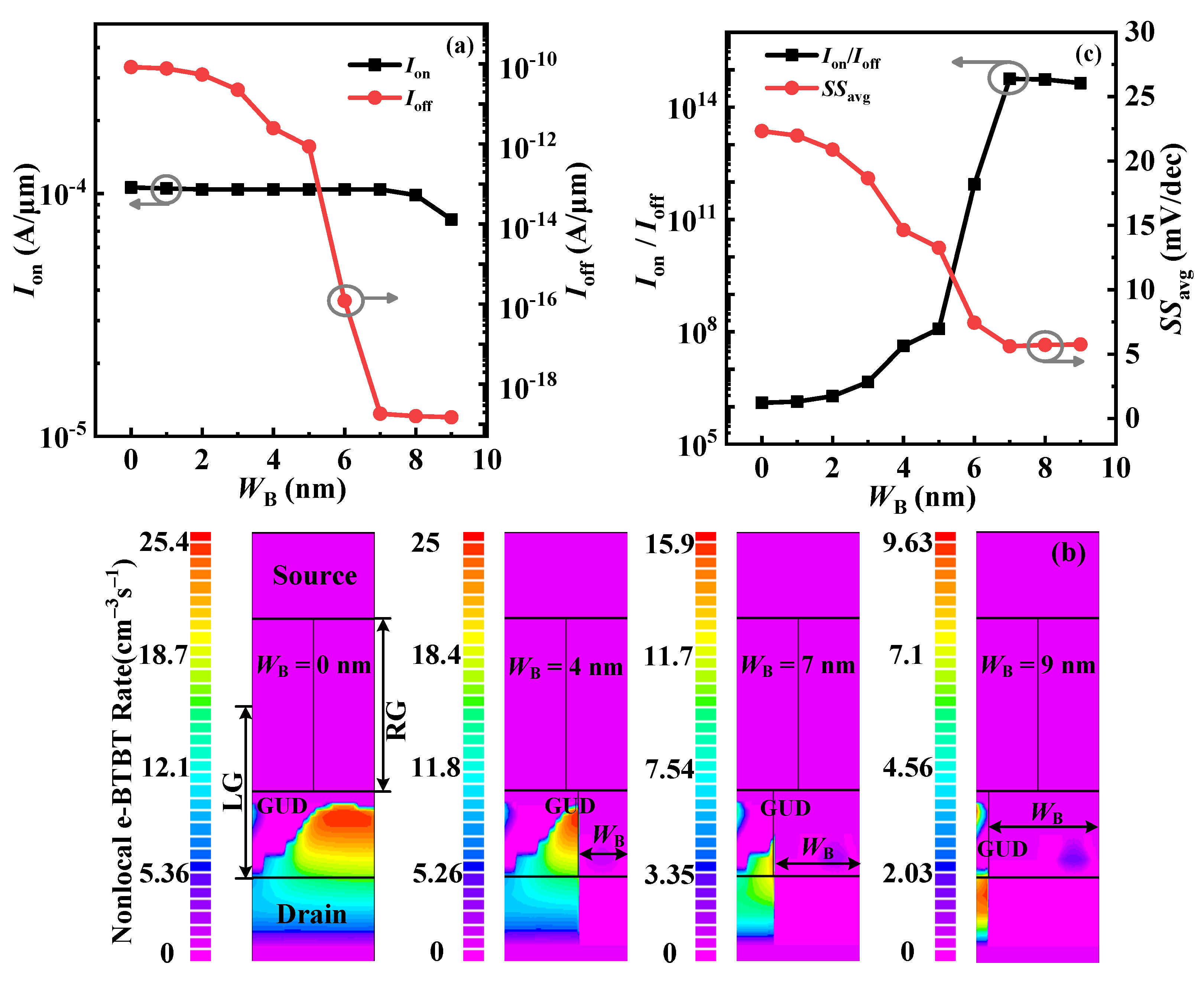
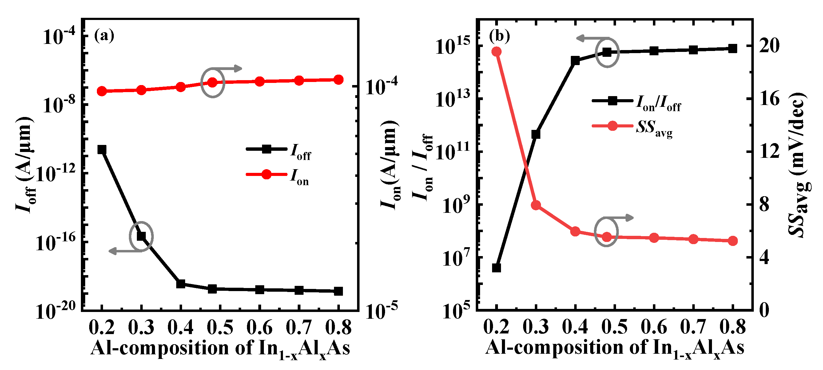
3.3. Effect of InAlAs-Block on VPB-EHBTFET

Here, the width and length (WB and LB) of the In0.52Al0.48As-block in the proposed VPB-EHBTFET are examined to optimize device performance. Figure 8a shows Ioff and Ion values under different WBs. Ioff gradually decreases with the increase in WB but basically maintains stability when WB > 7 nm, which can be explained by the contour plots of the non-local e-BTBT rate shown in Figure 8b. It is found that both the distribution range and magnitude of the non-local e-BTBT rate reduce with the increase in WB, which can demonstrate that the increasing WB helps to inhibit the P-tunneling in the right side of the GUD region caused by the P+-pocket, thereby lowering the Ioff. When WB = 7 nm, the non-local e-BTBT rate falls sharply due to complete suppression of this type of P-tunneling, thus resulting in several orders of magnitude reduction in Ioff. As WB goes beyond 7 nm, the In0.52Al0.48As-block begins to suppress the P-tunneling in the left side of the GUD region so as to further reduce the non-local e-BTBT rate. Since the λ of the P-tunneling in the left-side channel is very long, the electron tunneling in this region is insignificant. As a result, Ioff is not sensitive to the change in WB. Moreover, Figure 8a shows that only when WB > 7 nm does Ion begin to decrease. This is because although the In0.52Al0.48As-block does not affect the L-tunneling in the GO region, when WB > 7 nm, it prevents the tunneling electrons in the left-side channel from drifting to the drain region. As shown in Figure 8c, with the increase in WB, SSavg and Ion/Ioff decreases and increases, respectively, but both take on the opposite trend when WB > 7 nm. Thus, the best choice of WB is 7 nm.
Next, the influence of LB on the device performance is investigated. It should be noted that all research results are obtained with the unchanged channel length. Figure 9a shows the Ioff and Ion values under different LBs. Ioff decreases first with the increase in LB but basically keeps stable when LB > 25 nm. Since the off-state P-tunneling in the right-side channel is affected by the In0.52Al0.48As-block, its energy band profiles can be calculated to interpret the trend of Ioff. It is observed from Figure 9b that there are two kinds of P-tunneling between the P+-pocket and the GUD region: (1) electrons tunnel from the valence band of the P+-pocket into the conduction band of In0.53Ga0.47As (CBS) (named PCT-tunneling), and (2) electrons tunnel from the valence band of the P+-pocket into the conduction band of In0.52Al0.48As (CBB) (named PBT-tunneling). Due to the wider Eg in the In0.52Al0.48As and the longer λ in the tunneling junction, the effect of PBT-tunneling on Ioff is negligible. When LB = 0 nm, only the PCT-tunneling exists in the tunneling junction, and its Δφ is the widest; thus, the maximum Ioff is generated. With the increase in LB, the Δφ of the PCT-tunneling and the PBT-tunneling (i.e., Δφ1 and Δφ2 in Figure 9b) decreases and increases, respectively, and disappears and saturates, respectively, when LB ≥ 25 nm. It follows that the PCT-tunneling is gradually suppressed with the increase in LB and eventually completely replaced by the PCB-tunneling when LB ≥ 25 nm, thereby resulting in the change trend of Ioff shown in Figure 9a. Furthermore, Figure 9a shows that Ion is immune to the change in LB, which is because the L-tunneling dominant in the on-state is not affected by the LB. Figure 9c shows that SSavg and Ion/Ioff have the same and opposite change trend as Ioff, respectively. This is because both parameters mainly depend on Ioff, which is closely related to LB. This research demonstrates that good device performance can be achieved when LB is not less than 25 nm.
To verify the superiority of the introduction of the In0.52Al0.48As-block, the device performance of the proposed VPB-EHBTFET under lattice mismatch was investigated, and corresponding simulation results are shown in Figure 10. In simulations, the composition of InGaAs is unchanged, while the Al composition (i.e., x) of the In1−xAlxAs-block changes from 0.2 to 0.8. Considering the strain caused by the lattice mismatch, a strained two-band zincblende model is included in simulations. As shown in Figure 10a, it is observed that the Ion is insensitive to x, but the Ioff decreases first with the increase in x and then basically remains unchanged when x ≥ 0.48, both of which can be interpreted by the tunneling mechanism. Based on the previous analyses, the In1−xAlxAs-block located in the right-side GUD region mainly controls the off-state P-tunneling. With the increase in x, the Eg of In1−xAlxAs increases. According to Equation (1), the increase in Eg benefits to reducing the Ptun, eventually reducing the Ioff. When x ≥ 0.48, electrons are difficult to tunnel into the drain across the In1−xAlxAs-block due to the long λ caused by the Eg, which makes the Ioff basically remain stable. It is found from Figure 10b that when x < 0.48, Ion/Ioff and SSavg increases and decreases with the increase in x, respectively. As x increases further, both parameters tend to be saturated. Comprehensive analysis shows that good device performance of VPB-EHBTFET can be achieved when x ≥ 0.48. However, the epitaxial layers with mismatched lattices are prone to defects during growth, which can affect the performance and lifespan of devices. Therefore, In0.52Al0.48As with x = 0.48 is the optimal choice because it matches the lattice of In0.53Ga0.47As.

4. Conclusions

To sum up, an In0.53Ga0.47As vertical EHBTFET with a P+-pocket and an In0.52Al0.48As-block (VPB-EHBTFET) is introduced and investigated by TCAD simulation. Numerical simulations indicate that the adoption of a P+-pocket and In0.52Al0.48As-block can make VPB-EHBTFET simultaneously possess good on-state and off-state performance. Corresponding indicator parameters are Ion of 1.04 × 10⁻⁴ A/μm, Ioff of 1.83 × 10⁻¹⁹ A/μm, Ion/Ioff of 5.7 × 10¹⁴, SSavg of 5.5 mV/dec, and a DIBL value of 7.5 mV/V. Through examining the influence of the P+-pocket on VPB-EHBTFET, it results that CP controls the device performance by affecting the L-tunneling, while WP can simultaneously regulate the λ and Δφ of the point tunneling and line tunneling to obtain the optimal on-state performance. Considering the changes in WB and LB, it is concluded that both mainly control Ioff through the suppression of the P-tunneling in the right-side channel. Moreover, through investigating the effect of the Al composition of the In1−xAlxAs-block on the device performance and considering the potential performance degradation caused by lattice mismatch during device manufacturing, the In0.52Al0.48As-block that matches the lattice of In0.53Ga0.47As is the optimal choice.

Author Contributions

Conceptualization, H.L.; methodology, H.L.; software, P.L.; validation, Y.L. (Yubin Li) and P.W.; formal analysis, P.W. and P.L.; investigation, Y.L. (Yubin Li) and P.L.; resources, L.P. and H.L.; data curation, Y.L. (Yao Li); writing—original draft preparation, H.L. and P.L.; writing—review and editing, H.L. and X.Z.; visualization, P.L. and X.Z.; supervision, P.W.; project administration, P.L. and X.Z.; funding acquisition, H.L. and W.Z. All authors have read and agreed to the published version of the manuscript.

Funding

This research was funded by the National Natural Science Foundation of China (Grant No. 62264008) and the Natural Science Foundation of Gansu Province (Grant Nos. 21JR7RA320 and 22JR11RA154).

Data Availability Statement

The data presented in this study are available on request from the corresponding author.

Conflicts of Interest

The authors declare no conflict of interest.

References

  1. Sarkar, D.; Xie, X.J.; Liu, W.; Cao, W.; Kang, J.H.; Gong, Y.J.; Kraemer, S.; Ajayan, P.M.; Banerjee, K. A subthermionic tunnel field-effect transistor with an atomically thin channel. Nature 2015, 526, 91–95. [Google Scholar] [CrossRef] [PubMed]
  2. Kumar, M.J.; Janardhanan, S. Doping-less tunnel field effect transistor: Design and investigation. IEEE Trans. Electron Devices 2013, 60, 3285–3290. [Google Scholar] [CrossRef]
  3. Yang, Z.N. Tunnel field-effect transistor with an L-shaped gate. IEEE Electron Device Lett. 2016, 37, 839–842. [Google Scholar] [CrossRef]
  4. Jiang, X.X.; Shi, X.Y.; Zhang, M.; Wang, Y.R.; Gu, Z.H.; Chen, L.; Zhu, H.; Zhang, K.; Sun, Q.Q.; Zhang, D.W. A symmetric tunnel field-effect transistor based on mos2/black phosphorus/mos2 nanolayered heterostructures. ACS Appl. Nano Mater. 2019, 2, 5674–5680. [Google Scholar] [CrossRef]
  5. Xu, J.; Jia, J.Y.; Lai, S.; Ju, J.; Lee, S.J. Tunneling field effect transistor integrated with black phosphorus-MoS2 junction and ion gel dielectric. Appl. Phys. Lett. 2017, 110, 033103. [Google Scholar] [CrossRef]
  6. Chava, P.; Fekri, Z.; Vekariya, Y.; Mikolajick, T.; Erbe, A. Band-to-band tunneling switches based on two-dimensional van der Waals heterojunctions. Appl. Phys. Rev. 2023, 10, 011318. [Google Scholar] [CrossRef]
  7. Guha, S.; Pachal, P. Heterojunction negative-capacitance tunnel-FET as a promising candidate for sub-0.4 V VDD digital logic circuits. IEEE Trans. Nanotechnol. 2021, 20, 576–583. [Google Scholar] [CrossRef]
  8. Hu, V.P.H.; Lin, H.H.; Lin, Y.K.; Hu, C.M. Optimization of negative-capacitance vertical-tunnel FET (NCVT-FET). IEEE Trans. Electron Devices 2020, 67, 2593–2599. [Google Scholar] [CrossRef]
  9. Li, H.; Xu, P.P.; Xu, L.; Zhang, Z.Y.; Lu, J. Negative capacitance tunneling field effect transistors based on monolayer arsenene, antimonene, and bismuthene. Semicond. Sci. Technol. 2019, 34, 085006. [Google Scholar] [CrossRef]
  10. Liu, H.; Yang, L.A.; Jin, Z.; Hao, Y. An In0.53Ga0.47As/In0.52Al0.48As Heterojunction Dopingless Tunnel FET with a Heterogate Dielectric for High Performance. IEEE Trans. Electron Devices 2019, 66, 3229–3235. [Google Scholar] [CrossRef]
  11. Tripathy, M.R.; Singh, A.K.; Baral, K.; Singh, P.K.; Jit, S. III-V/Si staggered heterojunction based source-pocket engineered vertical TFETs for low power applications. Superlattices Microstruct. 2020, 142, 106494. [Google Scholar] [CrossRef]
  12. Ameen, T.A.; Ilatikhameneh, H.; Fay, P.; Seabaugh, A.; Rahman, R.; Klimeck, G. Alloy engineered nitride tunneling field-effect transistor: A solution for the challenge of heterojunction tfets. IEEE Trans. Electron Devices 2019, 66, 736–742. [Google Scholar] [CrossRef]
  13. Memisevic, E.; Svensson, J.; Lind, E.; Wernersson, L.E. Vertical nanowire TFETs with channel diameter down to 10 nm and point S MIN of 35 mV/decade. IEEE Electron Device Lett. 2018, 39, 1089–1091. [Google Scholar] [CrossRef]
  14. Kumar, N.; Raman, A. Performance Assessment of the Charge-Plasma-Based Cylindrical GAA Vertical Nanowire TFET With Impact of Interface Trap Charges. IEEE Trans. Electron Devices 2019, 66, 4453–4460. [Google Scholar] [CrossRef]
  15. Kumar, N.; Raman, A. Prospective sensing applications of novel heteromaterial based dopingless nanowire-TFET at low operating voltage. IEEE Trans. Nanotechnol. 2020, 19, 527–534. [Google Scholar] [CrossRef]
  16. Cherik, I.C.; Mohammadi, S. Germanium-source L-shaped TFET with dual in-line tunneling junction. Appl. Phys. A 2021, 127, 525. [Google Scholar] [CrossRef]
  17. Xie, H.W.; Liu, H.X. Design and investigation of a dual source and U-shaped gate TFET with n buffer and SiGe pocket. AIP Adv. 2020, 10, 055125. [Google Scholar] [CrossRef]
  18. Li, W.; Jia, Q.R.; Pan, Y.M.; Chen, X.A.; Yin, Y.; Wu, Y.P.; Wang, Y.C.; Wen, Y.; Wang, C.; Wang, S.X. A T-shaped gate tunneling field effect transistor with negative capacitance, super-steep subthreshold swing. Nanotechnology 2021, 32, 395202. [Google Scholar] [CrossRef] [PubMed]
  19. LattanzioL, L.; Michielis, D.; Ionescu, A.M. The electron–hole bilayer tunnel FET. Solid-State Electron. 2012, 74, 85–90. [Google Scholar] [CrossRef]
  20. Padilla, J.L.; Medina-Bailon, C.; Alper, C.; Gamiz, F.; Ionescuet, A.M. Confinement-induced InAs/GaSb heterojunction electron–hole bilayer tunneling field-effect transistor. Appl. Phys. Lett. 2018, 112, 182101. [Google Scholar] [CrossRef]
  21. Anam, A.; Kumar, N.; Amin, S.I.; Prasad, D.; Anand, S. Charge-plasma based symmetrical-gate complementary electron–hole bilayer TFET with improved performance for sub-0.5 V operation. Semicond. Sci. Technol. 2023, 38, 015012. [Google Scholar] [CrossRef]
  22. Ahangari, Z. Design and performance optimization of thin film tin monoxide (SnO)/silicon electron–hole bilayer tunnel field-effect transistor. J. Comput. Electron. 2020, 19, 1485–1493. [Google Scholar] [CrossRef]
  23. Alper, C.; Palestri, P.; Padilla, J.L.; Ionescu, A.M. Underlap counterdoping as an efficient means to suppress lateral leakage in the electron–hole bilayer tunnel FET. Semicond. Sci. Technol. 2016, 31, 045001. [Google Scholar] [CrossRef]
  24. Jeong, W.J.; Kim, T.K.; Moon, J.M.; Park, M.G.; Yoon, Y.G.; Hwang, B.W.; Choi, W.Y.; Shin, M.; Lee, S.H. Germanium electron–hole bilayer tunnel field-effect transistors with a symmetrically arranged double gate. Semicond. Sci. Technol. 2015, 30, 035021. [Google Scholar] [CrossRef]
  25. Padilla, J.L.; Medina-Bailon, C.; Navarro, C.; Alper, C.; Gamiz, F.; Ionescu, A.M. Analysis of the heterogate electron–hole bilayer tunneling field-effect transistor with partially doped channels: Effects on tunneling distance modulation and occupancy probabilities. IEEE Trans. Electron Devices 2018, 65, 339–346. [Google Scholar] [CrossRef]
  26. Ashita; Loan, S.A.; Alharbi, A.G.; Rafat, M. Ambipolar leakage suppression in electron–hole bilayer TFET: Investigation and analysi. J. Comput. Electron. 2018, 17, 977–985. [Google Scholar] [CrossRef]
  27. Ahangari, Z. Performance investigation of steep-slope core–shell nanotube indium nitride electron–hole bilayer tunnel field effect transistor. Appl. Phys. A Mater. Sci. Process. 2019, 125, 405. [Google Scholar] [CrossRef]
  28. Kim, S.; Choi, W.Y.; Park, B.G. Vertical-Structured Electron-Hole Bilayer Tunnel Field-Effect Transistor for Extremely Low-Power Operation with High Scalability. IEEE Trans. Electron Devices 2018, 65, 2010–2015. [Google Scholar] [CrossRef]
  29. Liu, H.; Zhang, W.T.; Wang, Z.X.; Li, Y.; Zhang, H.W. OFF-State Leakage Suppression in Vertical Electron–Hole Bilayer TFET Using Dual-Metal Left-Gate and N+-Pocket. Materials 2022, 15, 6924. [Google Scholar] [CrossRef]
  30. Iida, R.; Kim, S.H.; Yokoyama, M.; Taoka, N.; Lee, S.H.; Takenaka, M.; Takagi, S. Planar-type In0.53Ga0.47As channel band-to-band tunneling metal-oxide-semiconductor field-effect transistors. J. Appl. Phys. 2011, 100, 124505. [Google Scholar] [CrossRef]
  31. Suzuki, R.; Taoka, N.; Yokoyama, M.; Lee, S.; Kim, S.H.; Hoshii, T.; Yasuda, T.; Jevasuwan, W.; Maeda, T.; Ichikawa, O.; et al. 1-nm-capacitance-equivalent-thickness HfO2/Al2O3/InGaAs metal-oxide-semiconductor structure with low interface trap density and low gate leakage current density. Appl. Phys. Lett. 2012, 100, 132906. [Google Scholar] [CrossRef]
  32. Zhou, G.L.; Lu, Y.Q.; Li, R.; Zhang, Q.; Hwang, W.S.; Liu, Q.M.; Vasen, T.; Chen, C.; Zhu, H.J.; Kuo, J.M.; et al. Vertical InGaAs/InP Tunnel FETs with Tunneling Normal to the Gate. IEEE Electron Device Lett. 2011, 32, 1516–1518. [Google Scholar] [CrossRef]
  33. Zhao, H.; Huang, J.; Chen, Y.T.; Yum, J.H.; Wang, Y.Z.; Zhou, F.; Xue, F.; Lee, J.C. Effects of gate-first and gate-last process on interface quality of In0.53Ga0.47As metal-oxide-semiconductor capacitors using atomic-layer-deposited Al2O3 and HfO2 oxides. Appl. Phys. Lett. 2009, 95, 253501. [Google Scholar] [CrossRef]
  34. Hueting, R.J.E.; Rajasekharan, B.; Salm, C.; Schmitz, J. The Charge Plasma P-N Diode. IEEE Electron Device Lett. 2008, 29, 1367–1369. [Google Scholar] [CrossRef]
  35. Lide, D.R. CRC Handbook of Chemistry and Physics, 89th ed.; Taylor and Francis: New York, NY, USA, 2008; p. 12. [Google Scholar]
Figure 1. Schematics of (a) V-EHBTFET; (b) VP-EHBTFET; and (c) VPB-EHBTFET.
Micromachines 14 02049 g001
Figure 2. Off-state energy band profiles for EHBTFETs along (a) A-A′, (b) B-B′, and (c) C-C′, respectively; (d) Ids-Vgs curves of EHBTFETs.
Micromachines 14 02049 g002
Figure 3. On-state energy bands for EHBTFETs along (a) A-A′, (b) B-B′, and (c) C-C′, respectively.
Micromachines 14 02049 g003
Figure 4. Nonlocal e-BTBT rates for EHBTFETs along (a) B-B′ in the off-state and (b) C-C′ in the on-state.
Micromachines 14 02049 g004
Figure 5. (a) The correlation between point SS and drain current of EHBTFETs; and (b) Ids-Vgs curves of EHBTFETs at Vds = 0.1 V and Vds = 0.5 V, respectively.
Micromachines 14 02049 g005
Figure 6. (a) The variation of Ion and Ioff with CP for VPB-EHBTFET; (b) off-state and (c) on-state energy band profiles along C-C′ for VPB-EHBTFET; and (d) the variation of Ion/Ioff and SSavg with CP for VPB-EHBTFET.
Micromachines 14 02049 g006
Figure 7. (a) The variation of Ion and Ioff with WP for VPB-EHBTFET; (b) the peak value of the nonlocal e-BTBT rate under different WPs for the P-tunneling in the left-side channel and the L-tunneling in the GO region, in the off-state; and (c) the variation of Ion/Ioff and SSavg with WP for VPB-EHBTFET.
Micromachines 14 02049 g007
Figure 8. (a) The variation of Ion and Ioff with WB for VPB-EHBTFET; (b) the contour plots of the nonlocal e-BTBT rate under different WBs for VPB-EHBTFET in the off-state; and (c) the variation of Ion/Ioff and SSavg with WB for VPB-EHBTFET.
Micromachines 14 02049 g008
Figure 9. (a) The variation of Ion and Ioff with LB for VPB-EHBTFET; (b) energy band profiles of VPB-EHBTFET under different LBs in the off-state; and (c) the variation of Ion/Ioff and SSavg with LB for VPB-EHBTFET.
Micromachines 14 02049 g009
Figure 10. (a) Ion and Ioff; (b) Ion/Ioff and SSavg, for VPB-EHBTFET under different Al compositions.
Micromachines 14 02049 g010
Table 1. Device structure parameters used in simulations.
ParametersValue
Source length (LS)50 nm
Gate/source space (LGS)50 nm
Left gate length (LLG)100 nm
Drain length (LD)50 nm
Right gate length (LRG)100 nm
HfO2 length (LHfO2)150 nm
P+-pocket length (Lp)100 nm
P+-pocket width (Wp)5 nm
InAlAs-block length (LB)50 nm
InAlAs-block width (WB)7 nm
SiO2 length (LSiO2)100 nm
Gate/drain space (LGD)50 nm
Bulk material width (W)10 nm
Dielectric width (Wox)2 nm
Left gate work-function4.5 eV
Right gate work-function5.3 eV
Table 2. Extracted parameters for three EHBTFETs.
DeviceIOFF (A/μm)ION (A/μm)ION/IOFFVth (V)SSavg (mV/dec)DIBL (mV/V)
V-EHBTFET2.29 × 10−161.84 × 10−58.0 × 10100.2630.2N/A
VP-EHBTFET8.37 × 10−111.04 × 10−41.2 × 1060.0622.17.5
VPB-EHBTFET1.83 × 10−191.04 × 10−45.7 × 10140.065.57.5
Disclaimer/Publisher’s Note: The statements, opinions and data contained in all publications are solely those of the individual author(s) and contributor(s) and not of MDPI and/or the editor(s). MDPI and/or the editor(s) disclaim responsibility for any injury to people or property resulting from any ideas, methods, instructions or products referred to in the content.

