
Design of Trench MIS Field Plate Structure for Edge Termination of GaN Vertical PN Diode


Abstract
:1. Introduction
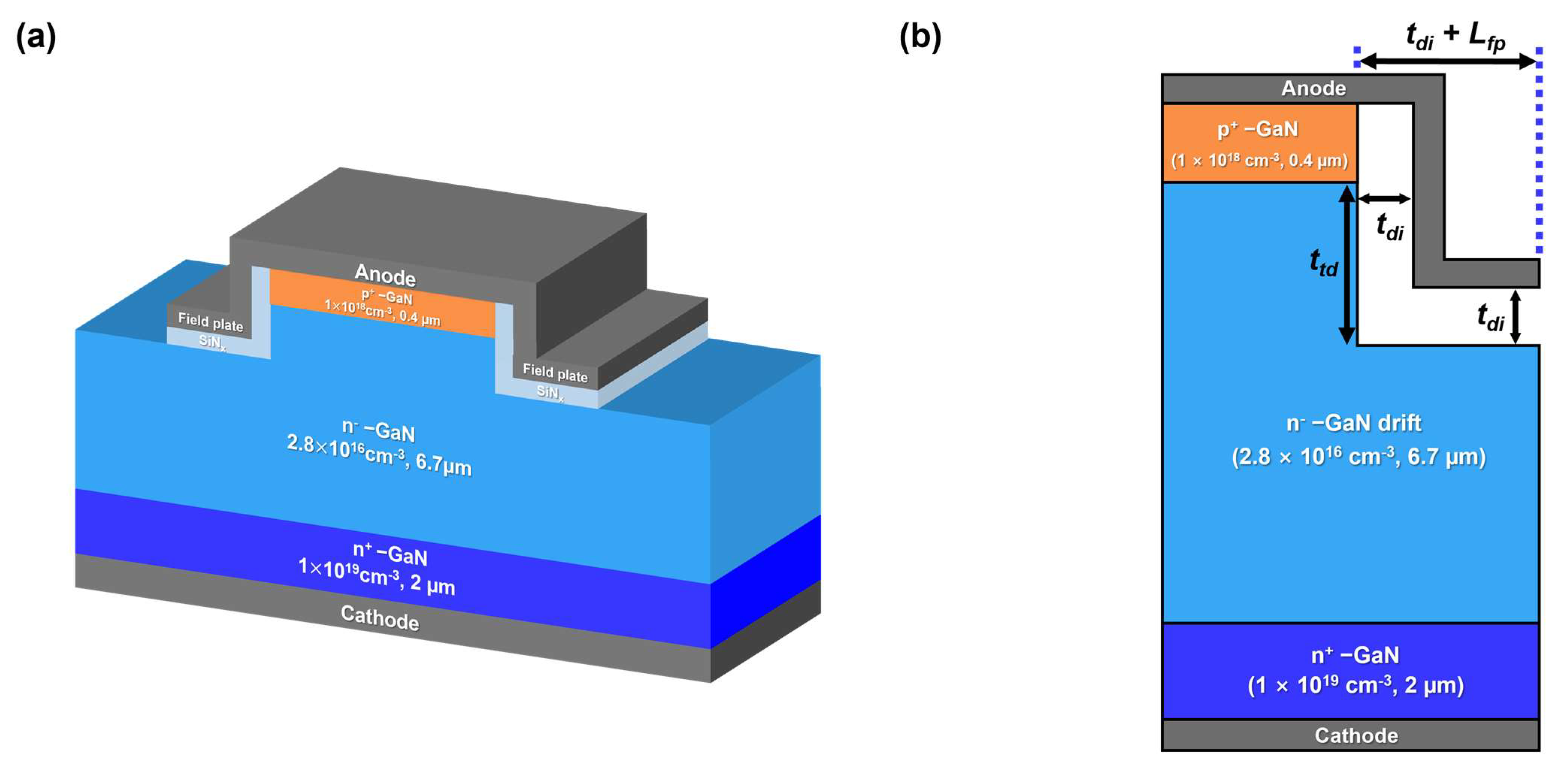
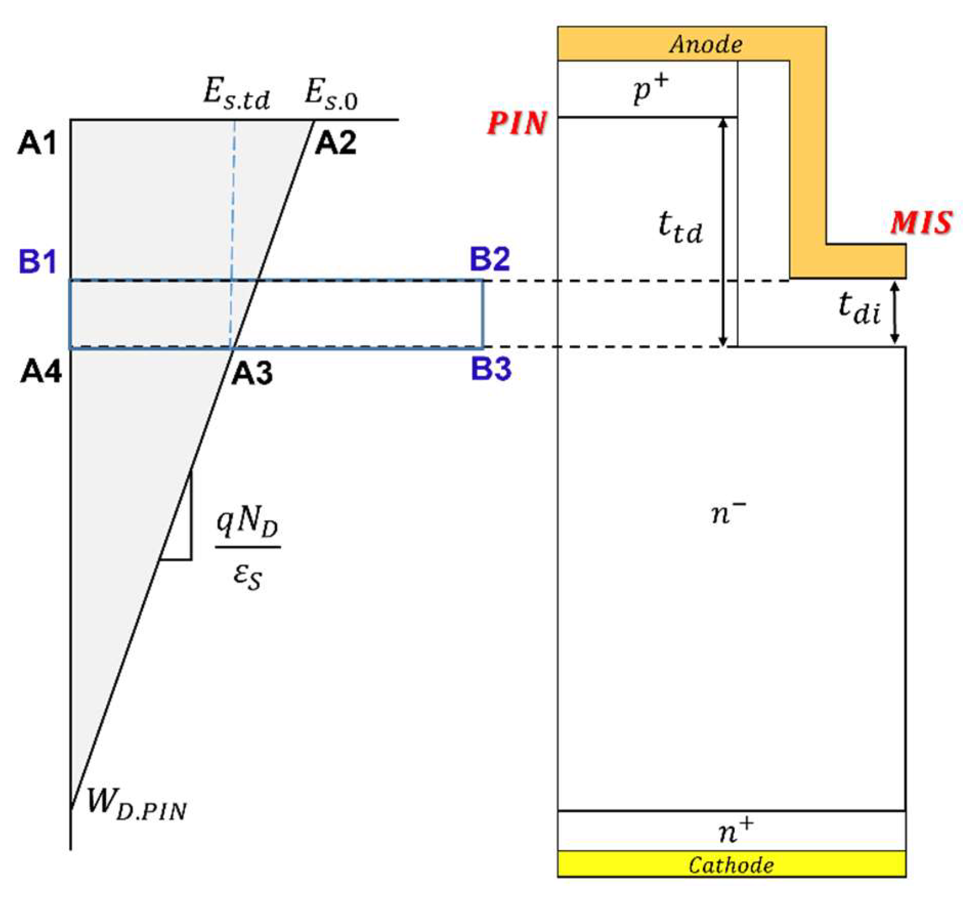
2. Device Structure
3. Boundary Conditions of Trench MIS FP
3.1. Punch-Through under MIS FP
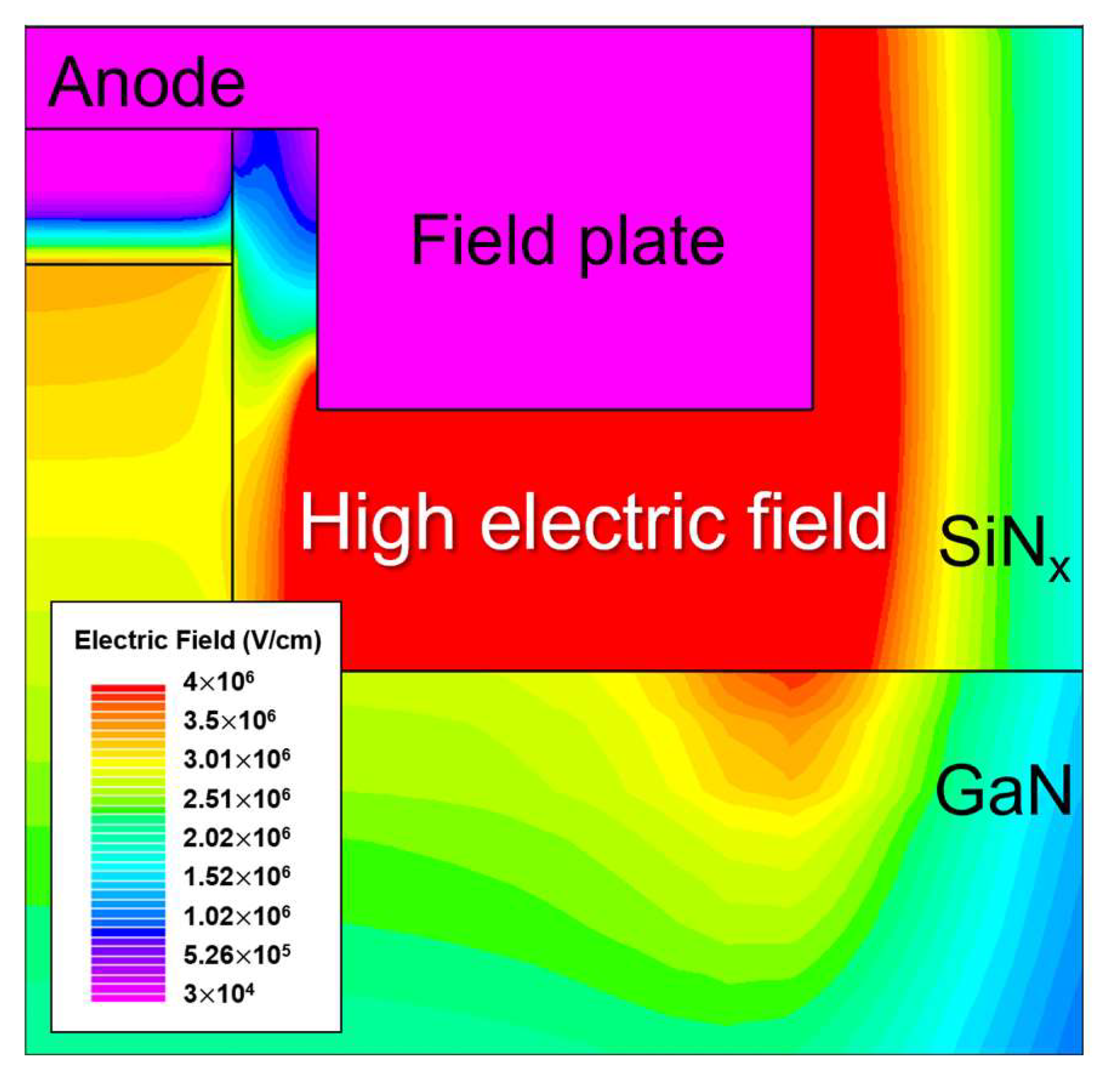
3.2. Avalanche Breakdown at the Surface under FP Edge
3.3. Dielectric Breakdown of MIS Region
4. Analytic Model
4.1. Design Approach for Optimum Trench MIS FP
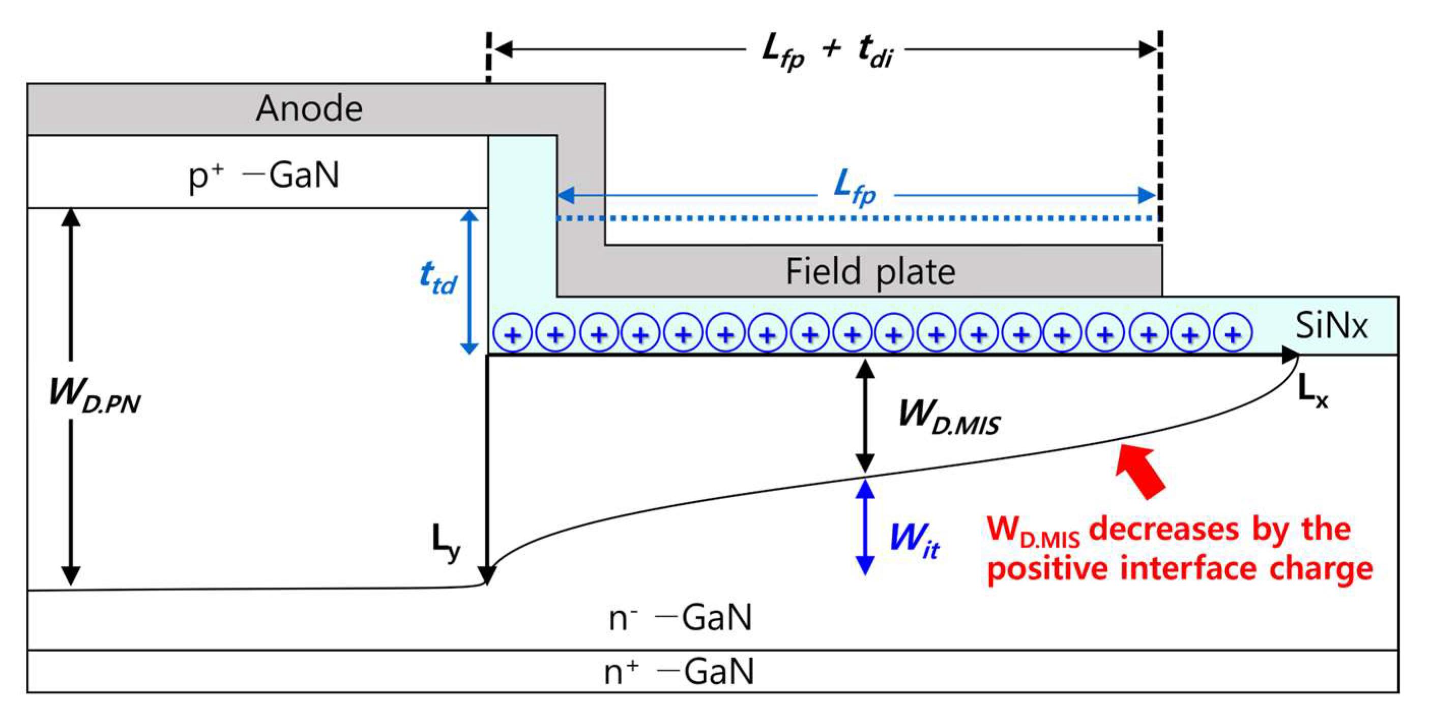
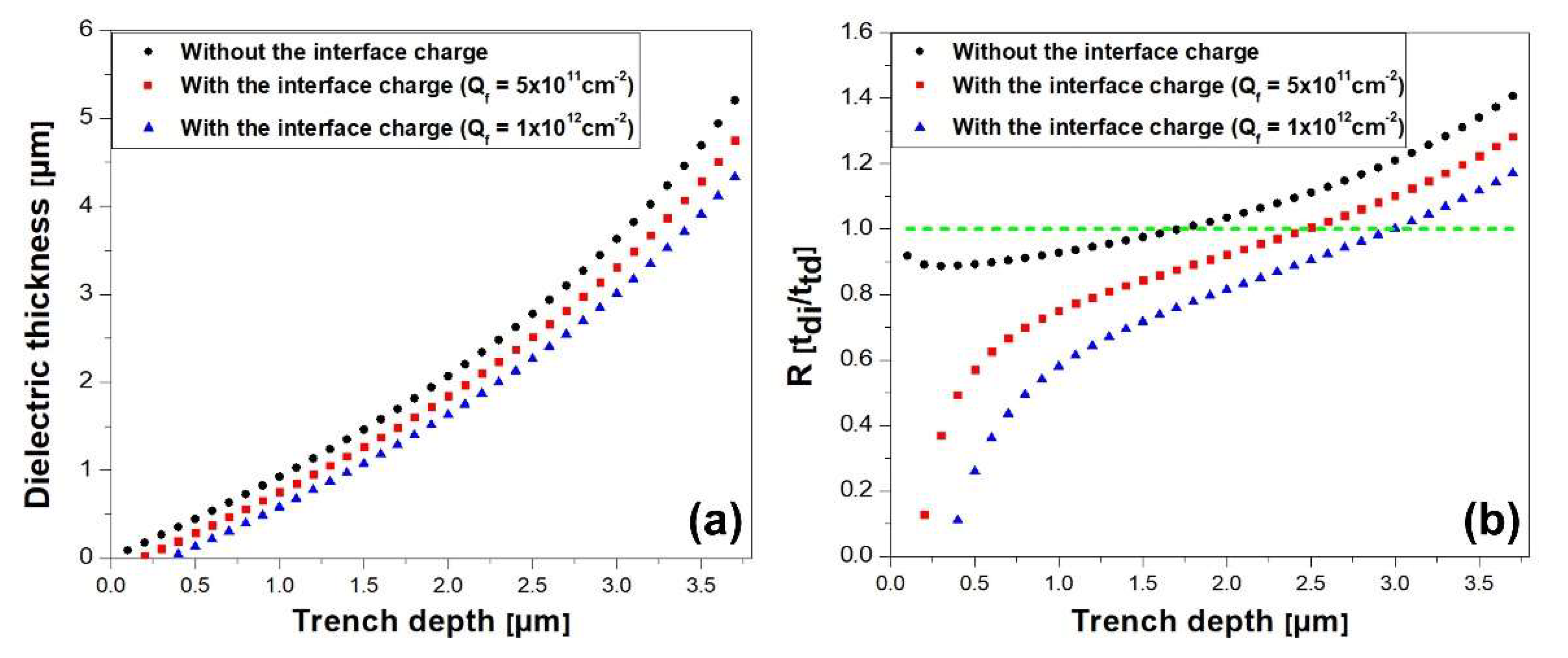
4.2. Interface Charge Effects
4.3. Maximum Allowed Electric Fields in GaN Surface and Dielectric Layer
5. Design of GaN PN Diode with a Trench MIS FP Structure
6. Conclusions
Author Contributions
Funding
Data Availability Statement
Conflicts of Interest
References
- Fu, H.; Fu, K.; Chowdhury, S.; Palacios, T.; Zhao, Y. Vertical GaN Power Devices: Device Principles and Fabrication Technologies—Part I. IEEE Trans. Electron Devices 2021, 68, 3200–3211. [Google Scholar] [CrossRef]
- Zhang, H.; Sun, Y.; Hu, K.; Yang, L.; Liang, K.; Xing, Z.; Wang, H.; Zhang, M.; Yu, H.; Fang, S. Boosted high-temperature electrical characteristics of AlGaN/GaN HEMTs with rationally designed compositionally graded AlGaN back barriers. Sci. China Inf. Sci. 2023, 66, 182405. [Google Scholar] [CrossRef]
- Sun, Y.; Zhang, H.; Yang, L.; Hu, K.; Xing, Z.; Liang, K.; Yu, H.; Fang, S.; Kang, Y.; Wang, D.; et al. Correlation Between Electrical Performance and Gate Width of GaN-Based HEMTs. IEEE Electron Device Lett. 2022, 43, 1199–1202. [Google Scholar] [CrossRef]
- Luo, D.; Liu, X.; Wang, R.; Li, X. A Review of Circuit Models for GaN Power Devices. In Proceedings of the 2023 IEEE 6th International Electrical and Energy Conference (CIEEC), Hefei, China, 12–14 May 2023; pp. 1461–1467. [Google Scholar]
- Chen, K.J.; Häberlen, O.; Lidow, A.; Lin Tsai, C.; Ueda, T.; Uemoto, Y.; Wu, Y. GaN-on-Si power technology: Devices and applications. IEEE Trans Electron Devices 2017, 64, 779–795. [Google Scholar] [CrossRef]
- Wen, H.; Liu, W.; Zhao, C. Evaluations of gan-on-si devices for power electronics applications. In Proceedings of the 2018 14th IEEE International Conference on Solid-State and Integrated Circuit Technology (ICSICT), Qingdao, China, 31 October–3 November 2018; IEEE: Piscataway, NJ, USA, 2018; pp. 1–4. [Google Scholar]
- Otsuka, N.; Kawai, Y.; Nagai, S. Recent progress in GaN devices for power and integrated circuit. In Proceedings of the 2017 IEEE 12th International Conference on ASIC (ASICON), Guiyang, China, 25–28 October 2017; IEEE: Piscataway, NJ, USA, 2017; pp. 928–931. [Google Scholar]
- Charitat, G. Voltage handling capability and termination techniques of silicon power semiconductor devices. In Proceedings of the 2001 BIPOLAR/BiCMOS Circuits and Technology Meeting (Cat. No. 01CH37212), Minneapolis, MN, USA, 30 September–2 October 2001; IEEE: Piscataway, NJ, USA, 2001; pp. 175–183. [Google Scholar]
- Temple, V.A. Junction termination extension (JTE), A new technique for increasing avalanche breakdown voltage and controlling surface electric fields in PN junctions. In Proceedings of the 1977 International Electron Devices Meeting, Washington, DC, USA, 5–7 December 1977; IEEE: Piscataway, NJ, USA, 1977; pp. 423–426. [Google Scholar]
- Kao, Y.C.; Wolley, E.D. High-voltage planar pn junctions. Proc. IEEE 1967, 55, 1409–1414. [Google Scholar] [CrossRef]
- Conti, F.; Conti, M. Surface breakdown in silicon planar diodes equipped with field plate. Solid-State Electron. 1972, 15, 93–105. [Google Scholar] [CrossRef]
- Rusu, A.; Bulucea, C. Deep-depletion breakdown voltage of silicon-dioxide/silicon MOS capacitors. IEEE Trans. Electron Devices 1979, 26, 201–205. [Google Scholar] [CrossRef]
- Stengl, R.; Gosele, U.; Fellinger, C.; Beyer, M.; Walesch, S. Variation of lateral doping as a field terminator for high-voltage power devices. IEEE Trans. Electron Devices 1986, 33, 426–428. [Google Scholar] [CrossRef]
- Park, C.; Hong, N.; Kim, D.J.; Lee, K. A new junction termination technique using ICP RIE for ideal breakdown voltages. In Proceedings of the 14th International Symposium on Power Semiconductor Devices and ICs, Santa Fe, NM, USA, 4–7 June 2002; IEEE: Piscataway, NJ, USA, 2002; pp. 257–260. [Google Scholar]
- Liu, S.; Cheng, X.; Zheng, L.; Sledziewski, T.; Erlbacher, T.; Sheng, L.; Yu, Y. Impact of the transition region between active area and edge termination on electrical performance of SiC MOSFET. Solid-State Electron. 2020, 171, 107873. [Google Scholar] [CrossRef]
- Varley, J.B.; Janotti, A.; Franchini, C.; Van de Walle, C.G. Role of self-trapping in luminescence and p-type conductivity of wide-band-gap oxides. Phys. Rev. B 2012, 85, 081109. [Google Scholar] [CrossRef]
- Baliga, B.J. Fundamentals of Power Semiconductor Devices; Springer: Berlin/Heidelberg, Germany, 2008. [Google Scholar]
- Kim, K.S.; Oh, C.S.; Han, M.S.; Kim, C.S.; Yang, G.M.; Yang, J.W.; Hong, C.; Youn, C.J.; Lim, K.Y.; Lee, H.J. Co-doping characteristics of Si and Zn with Mg in p-type GaN. Mater. Res. Soc. Internet J. Nitride Semicond. Res. 2000, 5, 322–328. [Google Scholar] [CrossRef]
- Narita, T.; Yoshida, H.; Tomita, K.; Kataoka, K.; Sakurai, H.; Horita, M.; Bockowski, M.; Ikarashi, N.; Suda, J.; Kachi, T. Progress on and challenges of p-type formation for GaN power devices. J. Appl. Phys. 2020, 128, 090901. [Google Scholar] [CrossRef]
- Kachi, T.; Narita, T.; Sakurai, H.; Matys, M.; Kataoka, K.; Hirukawa, K.; Sumida, K.; Horita, M.; Ikarashi, N.; Sierakowski, K. Process engineering of GaN power devices via selective-area p-type doping with ion implantation and ultra-high-pressure annealing. J. Appl. Phys. 2022, 132, 130901. [Google Scholar] [CrossRef]
- Jacobs, A.G.; Feigelson, B.N.; Hite, J.K.; Gorsak, C.A.; Luna, L.E.; Anderson, T.J.; Kub, F.J. Polarity dependent implanted p-type dopant activation in GaN. Jpn. J. Appl. Phys. 2019, 58, SCCD07. [Google Scholar] [CrossRef]
- Birkle, U.; Fehrer, M.; Kirchner, V.; Einfeldt, S.; Hommel, D.; Strauf, S.; Michler, P.; Gutowski, J. Studies on carbon as alternative P-type dopant for gallium nitride. MRS Online Proc. Libr. (OPL) 1998, 537, G5.6. [Google Scholar] [CrossRef]
- Yang, C.; Luo, X.; Zhang, A.; Deng, S.; Ouyang, D.; Peng, F.; Wei, J.; Zhang, B.; Li, Z. AlGaN/GaN MIS-HEMT with AlN interface protection layer and trench termination structure. IEEE Trans. Electron Devices 2018, 65, 5203–5207. [Google Scholar] [CrossRef]
- Nelson, T.; Pandey, P.; Georgiev, D.G.; Hontz, M.R.; Koehler, A.D.; Hobart, K.D.; Anderson, T.J.; Ildefonso, A.; Khanna, R. Hybrid Edge Termination in Vertical GaN: Approximating Beveled Edge Termination via Discrete Implantations. IEEE Trans. Electron Devices 2022, 69, 6940–6947. [Google Scholar] [CrossRef]
- Pandey, P.; Nelson, T.M.; Collings, W.M.; Hontz, M.R.; Georgiev, D.G.; Koehler, A.D.; Anderson, T.J.; Gallagher, J.C.; Foster, G.M.; Jacobs, A. A simple edge termination design for vertical GaN PN diodes. IEEE Trans. Electron Devices 2022, 69, 5096–5103. [Google Scholar] [CrossRef]
- Matys, M.; Ishida, T.; Nam, K.P.; Sakurai, H.; Narita, T.; Uesugi, T.; Bockowski, M.; Suda, J.; Kachi, T. Mg-implanted bevel edge termination structure for GaN power device applications. Appl. Phys. Lett. 2021, 118, 093502. [Google Scholar] [CrossRef]
- Krishna, D.V.; Panchal, A.; Sharma, E.; Dalal, S. Trench edge termination in a GaN-based power device. Mater. Today Proc. 2023, 79, 219–222. [Google Scholar] [CrossRef]
- Yang, W.; Feng, H.; Liu, Y.; Fang, X.; Onozawa, Y.; Tanaka, H.; Mitsuzuka, K.; Sin, J.K. A new 1200 V-class edge termination structure with trench double field plates for high dV/dt performance. In Proceedings of the 2017 29th International Symposium on Power Semiconductor Devices and IC’s (ISPSD), Sapporo, Japan, 28 May–1 June 2017; IEEE: Piscataway, NJ, USA, 2017; pp. 109–112. [Google Scholar]
- Yang, W.; Feng, H.; Fang, X.; Liu, Y.; Onozawa, Y.; Tanaka, H.; Sin, J.K. Design and characterization of sloped-field-plate enhanced trench edge termination. IEEE Trans. Electron Devices 2016, 64, 728–734. [Google Scholar] [CrossRef]
- Cao, Y.; Pomeroy, J.W.; Uren, M.J.; Yang, F.; Wang, J.; Fay, P.; Kuball, M. Edge termination in vertical GaN diodes: Electric field distribution probed by second harmonic generation. Appl. Phys. Lett. 2022, 120, 132104. [Google Scholar] [CrossRef]
- Liu, Y.; Yang, W.; Feng, H.; Onozawa, Y.; Wakimoto, S.; Fujishima, N.; Sin, J.K. Trench field plate engineering for high efficient edge termination of 1200 V-class SiC devices. In Proceedings of the 2019 31st International Symposium on Power Semiconductor Devices and ICs (ISPSD), Shanghai, China, 19–23 May 2019; IEEE: Piscataway, NJ, USA, 2019; pp. 143–146. [Google Scholar]
- Krishna, A.; Raj, A.; Hatui, N.; Keller, S.; Denbaars, S.; Mishra, U.K. Acceptor traps as the source of holes in p-type N-polar GaN/(AlN/AlGaN) superlattices. Appl. Phys. Lett. 2022, 120, 242106. [Google Scholar] [CrossRef]
- Arakawa, Y.; Ueno, K.; Kobayashi, A.; Ohta, J.; Fujioka, H. High hole mobility p-type GaN with low residual hydrogen concentration prepared by pulsed sputtering. APL Mater. 2016, 4, 086103. [Google Scholar] [CrossRef]
- Malinverni, M.; Lamy, J.; Martin, D.; Feltin, E.; Dorsaz, J.; Castiglia, A.; Rossetti, M.; Duelk, M.; Vélez, C.; Grandjean, N. Low temperature p-type doping of (Al) GaN layers using ammonia molecular beam epitaxy for InGaN laser diodes. Appl. Phys. Lett. 2014, 105, 241103. [Google Scholar] [CrossRef]
- Liliental-Weber, Z.; Benamara, M.; Swider, W.; Washburn, J.; Grzegory, I.; Porowski, S.; Dupuis, R.D.; Eiting, C.J. Mg segregation, difficulties of p-doping in GaN. Mater. Res. Soc. Internet J. Nitride Semicond. Res. 2000, 5, 500–506. [Google Scholar] [CrossRef]
- Eiting, C.J.; Grudowski, P.A.; Dupuis, R.D. P-and N-type doping of GaN and AlGaN epitaxial layers grown by metalorganic chemical vapor deposition. J. Electron. Mater. 1998, 27, 206–209. [Google Scholar] [CrossRef]
- Chung, S.; Han, S. Design curves of breakdown voltage at field plate edge and effect of interface charge. Microelectron. J. 2002, 33, 399–402. [Google Scholar] [CrossRef]
- Bordoloi, S.; Ray, A.; Trivedi, G. Access region stack engineering for mitigation of degradation in algan/gan hemts with field plate. IEEE Trans. Device Mater. Reliab. 2022, 22, 73–84. [Google Scholar] [CrossRef]
- Onodera, H.; Horio, K. Physics-based simulation of field-plate effects on breakdown characteristics in AlGaN/GaN HEMTs. In Proceedings of the 2012 7th European Microwave Integrated Circuit Conference, Amsterdam, The Netherlands, 29–30 October 2012; IEEE: Piscataway, NJ, USA, 2012; pp. 401–404. [Google Scholar]
- Chen, T.; Zhou, Q.; Wei, D.; Dong, C.; Chen, W.; Zhang, B. Physics-based 2-D analytical model for field-plate engineering of AlGaN/GaN power HFET. IEEE Trans. Electron Devices 2018, 66, 116–125. [Google Scholar] [CrossRef]
- Kumar, J.R.; Nirmal, D.; Du John, H.V.; Franklin, S.A.; Samuel, G. Design and Simulation of a T-gated AlGaN/GaN HEMT with Added Mini Field Plate. In Proceedings of the 2022 3rd International Conference on Electronics and Sustainable Communication Systems (ICESC), Coimbatore, India, 17–19 August 2022; IEEE: Piscataway, NJ, USA, 2022; pp. 303–306. [Google Scholar]
- Karmalkar, S.; Mishra, U.K. Enhancement of breakdown voltage in AlGaN/GaN high electron mobility transistors using a field plate. IEEE Trans. Electron Devices 2001, 48, 1515–1521. [Google Scholar] [CrossRef]
- Chung, S.K.; Yoo, D.C.; Choi, Y.I. An analytical method for two-dimensional field distribution of a MOS structure with a finite field plate. IEEE Trans. Electron Devices 1995, 42, 192–194. [Google Scholar] [CrossRef]


| Structures | P+ GaN | N− GaN | N+ GaN |
|---|---|---|---|
| Thickness (µm) | 0.4 | 6.7 | 2 |
| Doping concentration (cm−3) | 1 × 10¹⁸ | 2.8 × 10¹⁶ | 1 × 10¹⁹ |
Disclaimer/Publisher’s Note: The statements, opinions and data contained in all publications are solely those of the individual author(s) and contributor(s) and not of MDPI and/or the editor(s). MDPI and/or the editor(s) disclaim responsibility for any injury to people or property resulting from any ideas, methods, instructions or products referred to in the content. |
© 2023 by the authors. Licensee MDPI, Basel, Switzerland. This article is an open access article distributed under the terms and conditions of the Creative Commons Attribution (CC BY) license (https://creativecommons.org/licenses/by/4.0/).
Share and Cite
Lee, S.-H.; Cha, H.-Y. Design of Trench MIS Field Plate Structure for Edge Termination of GaN Vertical PN Diode. Micromachines 2023, 14, 2005. https://doi.org/10.3390/mi14112005
Lee S-H, Cha H-Y. Design of Trench MIS Field Plate Structure for Edge Termination of GaN Vertical PN Diode. Micromachines. 2023; 14(11):2005. https://doi.org/10.3390/mi14112005
Chicago/Turabian StyleLee, Sung-Hoon, and Ho-Young Cha. 2023. "Design of Trench MIS Field Plate Structure for Edge Termination of GaN Vertical PN Diode" Micromachines 14, no. 11: 2005. https://doi.org/10.3390/mi14112005
APA StyleLee, S.-H., & Cha, H.-Y. (2023). Design of Trench MIS Field Plate Structure for Edge Termination of GaN Vertical PN Diode. Micromachines, 14(11), 2005. https://doi.org/10.3390/mi14112005