
Enhanced Graphene Based Electronically Tunable Phase Shifter


Abstract
:1. Introduction
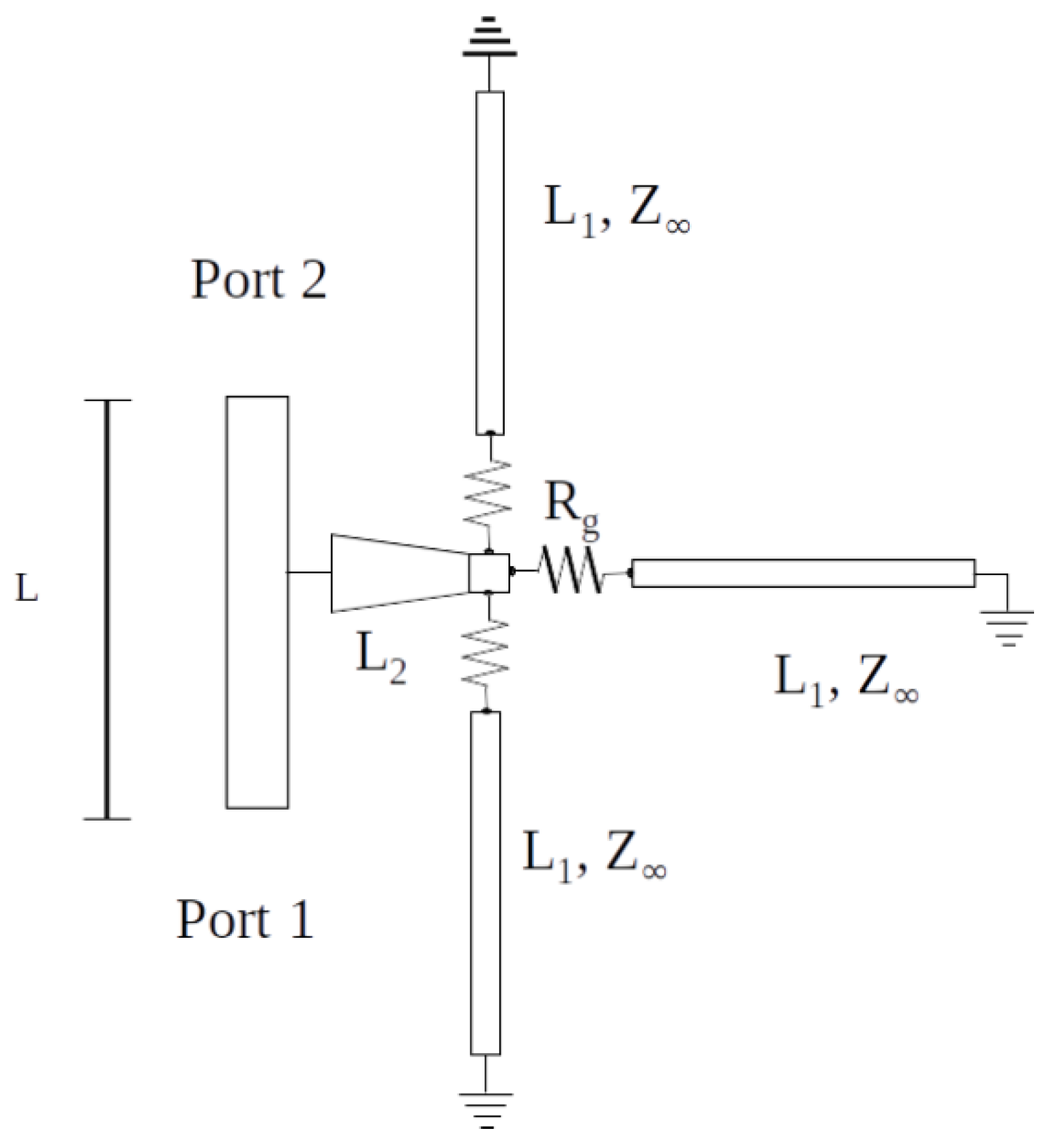
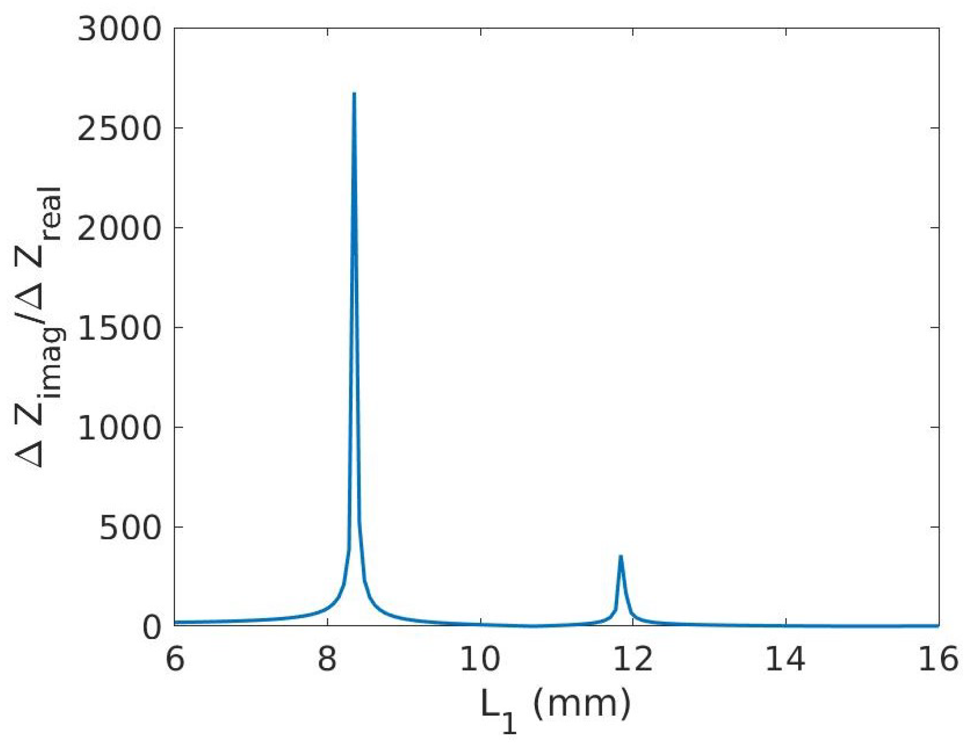
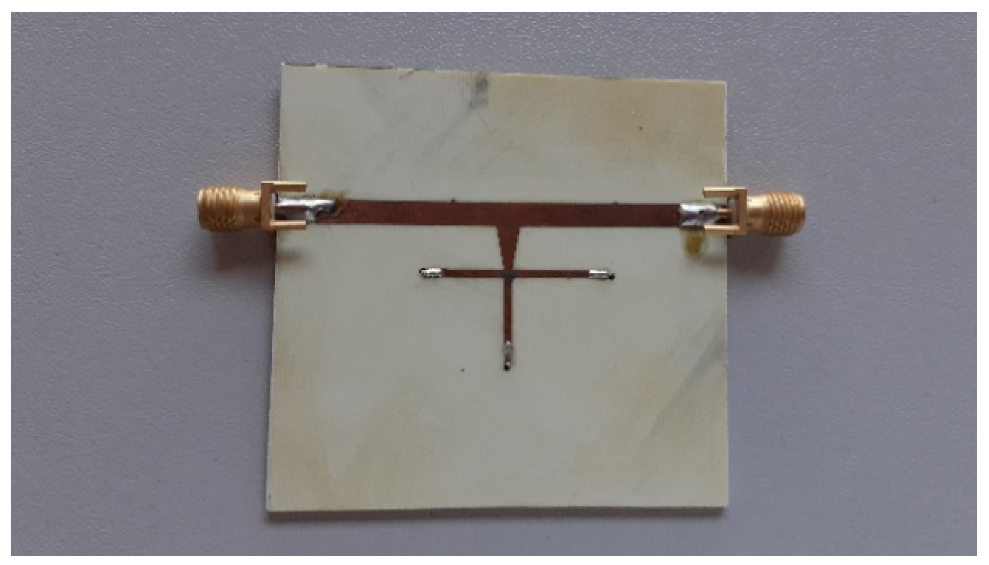
2. Materials and Methods
3. Graphene Flakes Analysis
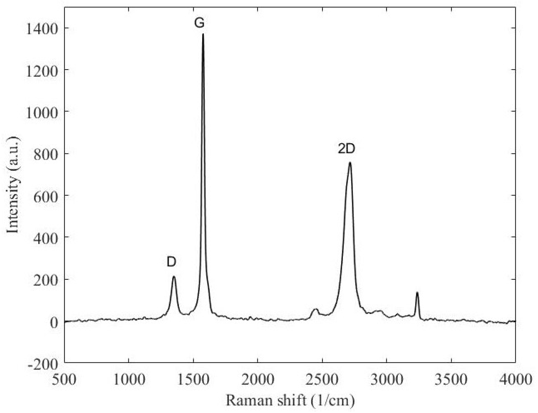
3.1. Raman Analysis
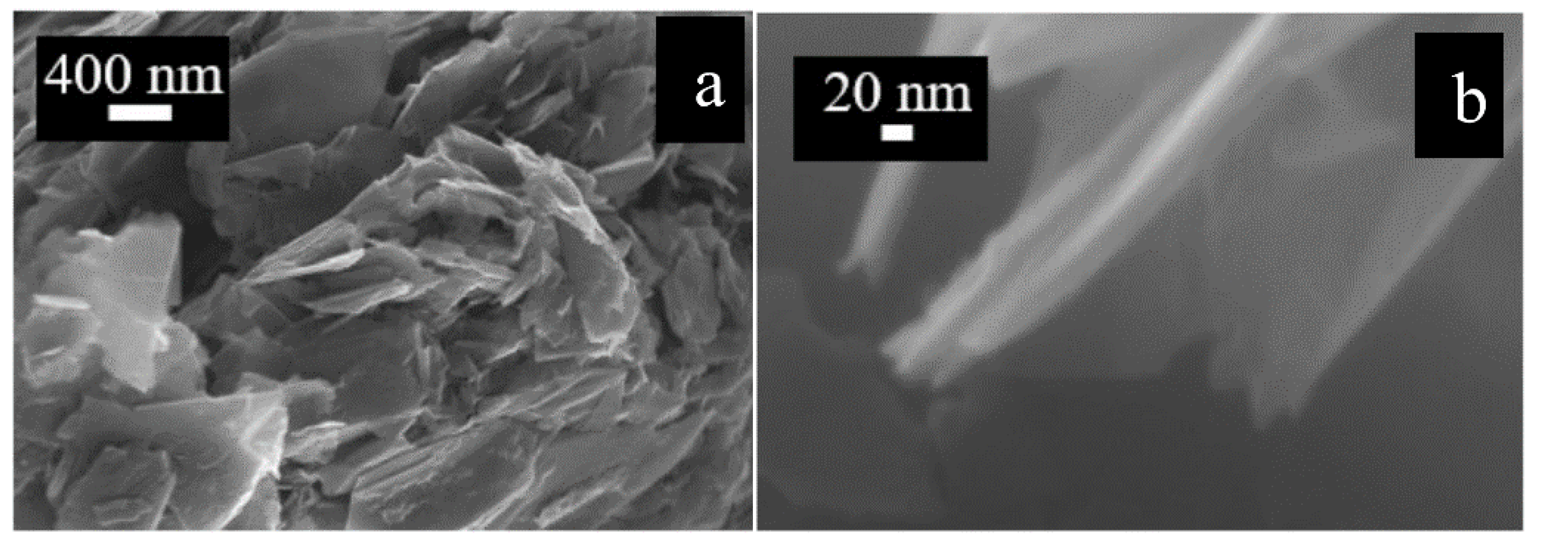
3.2. Fesem Analysis
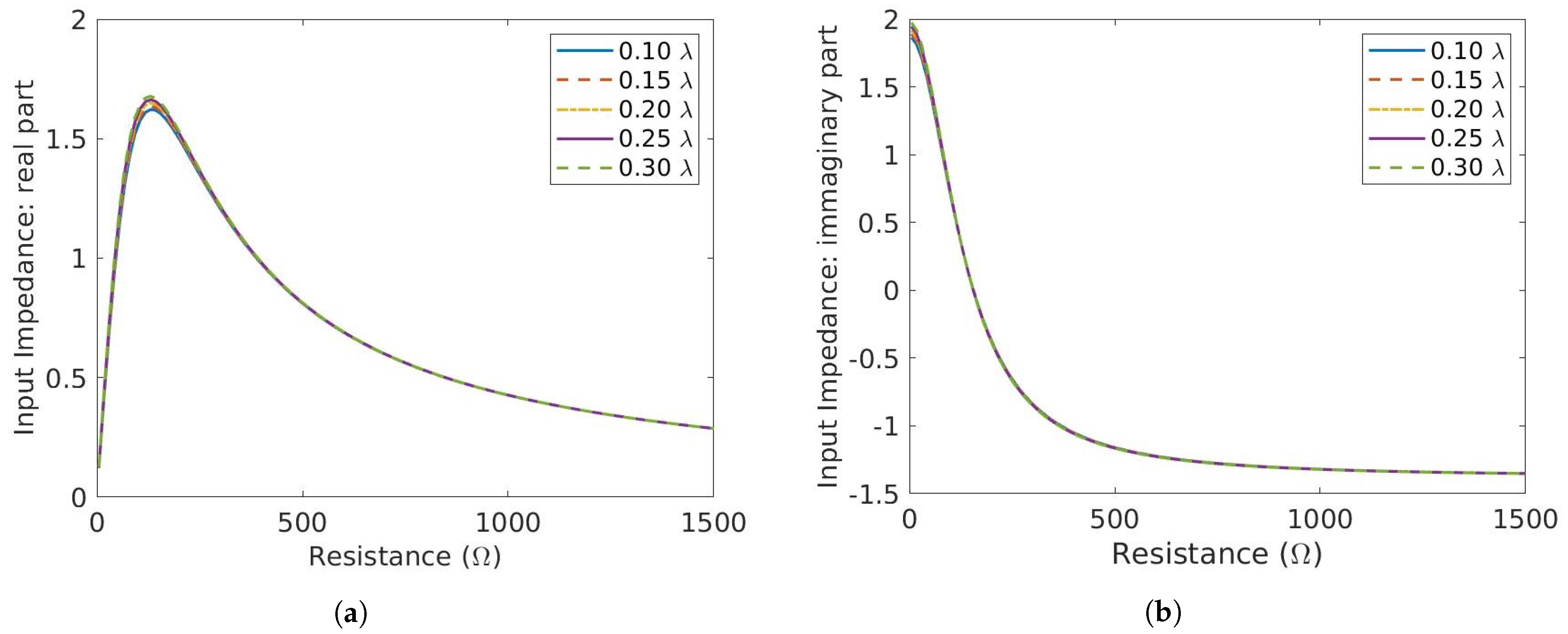
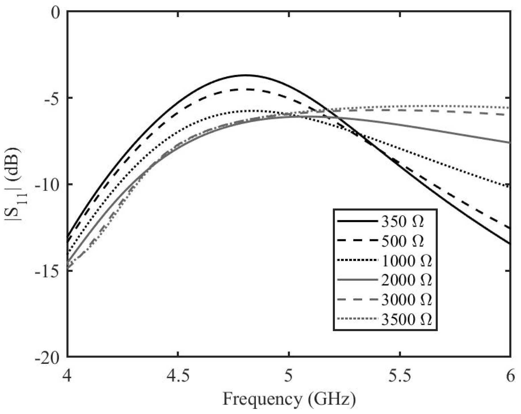
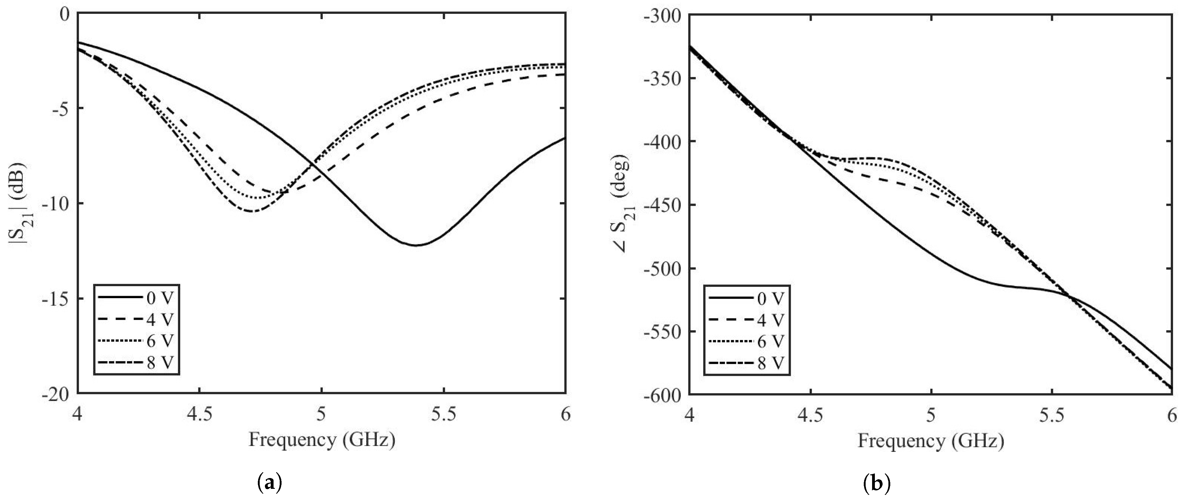
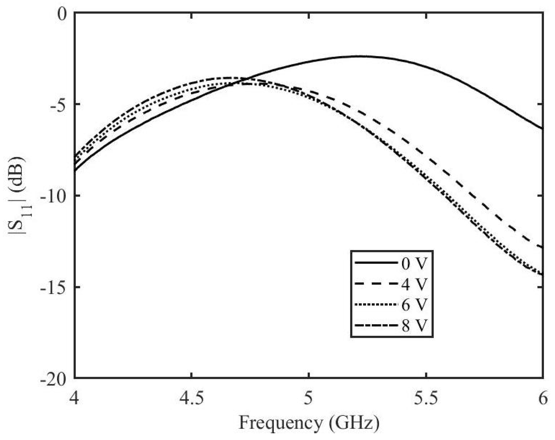
4. Results
5. Conclusions
Author Contributions
Funding
Data Availability Statement
Conflicts of Interest
References
- Wang, Y.; Zhang, L.; Hou, H.; Xu, W.; Duan, G.; He, S.; Liu, K.; Jiang, S. Recent progress in carbon-based materials for supercapacitor electrodes: A review. J. Mater. Sci. 2021, 56, 173–200. [Google Scholar] [CrossRef]
- Yang, Y.; Asiri, A.M.; Tang, Z.; Du, D.; Lin, Y. Graphene based materials for biomedical applications. Mater. Today 2013, 16, 365–373. [Google Scholar] [CrossRef]
- Geim, A.K. Graphene: Status and prospects. Science 2009, 324, 1530–1534. [Google Scholar] [CrossRef] [PubMed]
- Neto, A.C.; Guinea, F.; Peres, N.M.; Novoselov, K.S.; Geim, A.K. The electronic properties of graphene. Rev. Mod. Phys. 2009, 81, 109. [Google Scholar] [CrossRef]
- Liu, J.; Xue, Y.; Zhang, M.; Dai, L. Graphene-based materials for energy applications. MRS Bull. 2012, 37, 1265–1272. [Google Scholar] [CrossRef]
- Oğuzer, T.; Altıntaş, A. Evaluation of the E-polarization focusing ability in Thz range for microsize cylindrical parabolic reflector made of thin dielectric layer sandwiched between graphene. IET Microw. Antennas Propag. 2021, 15, 1240–1248. [Google Scholar] [CrossRef]
- Yevtushenko, F.O.; Dukhopelnykov, S.V.; Zinenko, T.L.; Rapoport, Y.G. Electromagnetic characterization of tuneable graphene-strips-on-substrate metasurface over entire THz range: Analytical regularization and natural-mode resonance interplay. IET Microw. Antennas Propag. 2021, 15, 1225–1239. [Google Scholar] [CrossRef]
- Lotfalizadeh, H.; Ghaffari-Miab, M. Dyadic Green’s function of partially filled graphene-loaded rectangular waveguides. IET Microw. Antennas Propag. 2021, 15, 1785–1798. [Google Scholar] [CrossRef]
- Lin, Z.C.; Zhang, Y.; Li, L.; Zhao, Y.T.; Chen, J.; Xu, K.D. Extremely wideband metamaterial absorber using spatial lossy transmission lines and resistively loaded high impedance surface. IEEE Trans. Microw. Theory Tech. 2023, 71, 3323–3332. [Google Scholar] [CrossRef]
- Cai, Y.; Huang, Y.; Feng, N.; Huang, Z. Improved Transformer-Based Target Matching of Terahertz Broadband Reflective Metamaterials with Monolayer Graphene. IEEE Trans. Microw. Theory Tech. 2023, 71, 3284–3293. [Google Scholar] [CrossRef]
- Karthik, V.; Selvakumar, P.; Senthil Kumar, P.; Vo, D.V.N.; Gokulakrishnan, M.; Keerthana, P.; Tamil Elakkiya, V.; Rajeswari, R. Graphene-based materials for environmental applications: A review. Environ. Chem. Lett. 2021, 19, 3631–3644. [Google Scholar] [CrossRef]
- Han, M.; Muhammad, Y.; Wei, Y.; Zhu, Z.; Huang, J.; Li, J. A review on the development and application of graphene based materials for the fabrication of modified asphalt and cement. Constr. Build. Mater. 2021, 285, 122885. [Google Scholar] [CrossRef]
- Liu, H.; Wang, P.; Wu, J.; Yan, X.; Yuan, X.; Zhang, Y.; Zhang, X. Switchable and dual-tunable multilayered terahertz absorber based on patterned graphene and vanadium dioxide. Micromachines 2021, 12, 619. [Google Scholar] [CrossRef] [PubMed]
- Chen, Z.; Cai, P.; Wen, Q.; Chen, H.; Tang, Y.; Yi, Z.; Wei, K.; Li, G.; Tang, B.; Yi, Y. Graphene Multi-Frequency Broadband and Ultra-Broadband Terahertz Absorber Based on Surface Plasmon Resonance. Electronics 2023, 12, 2655. [Google Scholar] [CrossRef]
- Zhang, J.; Tao, S.; Yan, X.; Zhang, X.; Guo, J.; Wen, Z. Dual-frequency polarized reconfigurable terahertz antenna based on graphene metasurface and TOPAS. Micromachines 2021, 12, 1088. [Google Scholar] [CrossRef]
- Yasir, M.; Fatikow, S.; Haenssler, O.C. Amplitude-phase variation in a graphene-based microstrip line. Micromachines 2022, 13, 1039. [Google Scholar] [CrossRef]
- Zhang, J.; Song, R.; Zhao, X.; Fang, R.; Zhang, B.; Qian, W.; Zhang, J.; Liu, C.; He, D. Flexible graphene-assembled film-based antenna for wireless wearable sensor with miniaturized size and high sensitivity. ACS Omega 2020, 5, 12937–12943. [Google Scholar] [CrossRef]
- Dragoman, M.; Neculoiu, D.; Dragoman, D.; Deligeorgis, G.; Konstantinidis, G.; Cismaru, A.; Coccetti, F.; Plana, R. Graphene for microwaves. IEEE Microw. Mag. 2010, 11, 81–86. [Google Scholar] [CrossRef]
- Hanson, G.W. Dyadic Green’s functions and guided surface waves for a surface conductivity model of graphene. J. Appl. Phys. 2008, 103, 064302. [Google Scholar] [CrossRef]
- Huang, X.; Leng, T.; Chang, K.H.; Chen, J.C.; Novoselov, K.S.; Hu, Z. Graphene radio frequency and microwave passive components for low cost wearable electronics. 2D Mater. 2016, 3, 025021. [Google Scholar] [CrossRef]
- Pierantoni, L.; Mencarelli, D.; Bozzi, M.; Moro, R.; Moscato, S.; Perregrini, L.; Micciulla, F.; Cataldo, A.; Bellucci, S. Broadband microwave attenuator based on few layer graphene flakes. IEEE Trans. Microw. Theory Tech. 2015, 63, 2491–2497. [Google Scholar] [CrossRef]
- Yasir, M.; Bistarelli, S.; Cataldo, A.; Bozzi, M.; Perregrini, L.; Bellucci, S. Voltage-controlled and input-matched tunable microstrip attenuators based on few-layer graphene. IEEE Trans. Microw. Theory Tech. 2019, 68, 701–710. [Google Scholar] [CrossRef]
- Yasir, M.; Bistarelli, S.; Cataldo, A.; Bozzi, M.; Perregrini, L.; Bellucci, S. Enhanced tunable microstrip attenuator based on few layer graphene flakes. IEEE Microw. Wirel. Compon. Lett. 2017, 27, 332–334. [Google Scholar] [CrossRef]
- Yasir, M.; Savi, P.; Bistarelli, S.; Cataldo, A.; Bozzi, M.; Perregrini, L.; Bellucci, S. A planar antenna with voltage-controlled frequency tuning based on few-layer graphene. IEEE Antennas Wirel. Propag. Lett. 2017, 16, 2380–2383. [Google Scholar] [CrossRef]
- Yasir, M.; Bistarelli, S.; Cataldo, A.; Bozzi, M.; Perregrini, L.; Bellucci, S. Tunable phase shifter based on few-layer graphene flakes. IEEE Microw. Wirel. Compon. Lett. 2018, 29, 47–49. [Google Scholar] [CrossRef]
- Yasir, M.; Savi, P. Dynamically Tunable Phase Shifter with Commercial Graphene Nanoplatelets. Micromachines 2020, 11, 600. [Google Scholar] [CrossRef]
- Rasappa, S.; Caridad, J.M.; Schulte, L.; Cagliani, A.; Borah, D.; Morris, M.A.; Bøggild, P.; Ndoni, S. High quality sub-10 nm graphene nanoribbons by on-chip PS-b-PDMS block copolymer lithography. RSC Adv. 2015, 5, 66711–66717. [Google Scholar] [CrossRef]
- Ferrari, A.C.; Meyer, J.C.; Scardaci, V.; Casiraghi, C.; Lazzeri, M.; Mauri, F.; Piscanec, S.; Jiang, D.; Novoselov, K.S.; Roth, S.; et al. Raman spectrum of graphene and graphene layers. Phys. Rev. Lett. 2006, 97, 187401. [Google Scholar] [CrossRef]


Disclaimer/Publisher’s Note: The statements, opinions and data contained in all publications are solely those of the individual author(s) and contributor(s) and not of MDPI and/or the editor(s). MDPI and/or the editor(s) disclaim responsibility for any injury to people or property resulting from any ideas, methods, instructions or products referred to in the content. |
© 2023 by the authors. Licensee MDPI, Basel, Switzerland. This article is an open access article distributed under the terms and conditions of the Creative Commons Attribution (CC BY) license (https://creativecommons.org/licenses/by/4.0/).
Share and Cite
Yasir, M.; Peinetti, F.; Savi, P. Enhanced Graphene Based Electronically Tunable Phase Shifter. Micromachines 2023, 14, 1877. https://doi.org/10.3390/mi14101877
Yasir M, Peinetti F, Savi P. Enhanced Graphene Based Electronically Tunable Phase Shifter. Micromachines. 2023; 14(10):1877. https://doi.org/10.3390/mi14101877
Chicago/Turabian StyleYasir, Muhammad, Fabio Peinetti, and Patrizia Savi. 2023. "Enhanced Graphene Based Electronically Tunable Phase Shifter" Micromachines 14, no. 10: 1877. https://doi.org/10.3390/mi14101877
APA StyleYasir, M., Peinetti, F., & Savi, P. (2023). Enhanced Graphene Based Electronically Tunable Phase Shifter. Micromachines, 14(10), 1877. https://doi.org/10.3390/mi14101877