Abstract
In this article, an innovative GaN-based trench current-aperture vertical electron transistor (CAVET) with a stepped doping microstructure is proposed and studied using Silvaco-ATLAS. According to the simulation and analyzed characteristics, the best performance renders a remarkable Baliga’s figure of merit (FOM) of 4.767 GW·cm2 owing to the modulation of the electric-field distribution. By adjusting the size of the stepped doping microstructure and doping concentration in the GaN drift, the maximum optimized result can achieve a relatively high breakdown voltage (BV) of 2523 V with a very low specific on-resistance (Ron,sp) of 1.34 mΩ·cm2, or the BV can be improved to 3024 V with a specific on-resistance (Ron,sp) of 2.08 mΩ·cm2. Compared with the conventional superjunction GaN-based trench CAVET, the newly demonstrated structure can achieve a 43% reduction in Ron,sp and increase by almost 20% the original BV. These results indicate the superiority of using the stepped doping microstructure in a trench CAVET to improve the BV and decrease Ron,sp, providing a reference for further development of GaN-based CAVETs.
1. Introduction
Over the past few decades, GaN-based devices went through rapid development, such as GaN MOSFETs, GaN Schottky diodes [1] and GaN photodetectors [2]. In the field of high-power applications, GaN-based power devices with a vertical structure attract much attention for their suitability in the fabrication of high-efficiency power converters [3]. Although typical lateral structures [4,5] dominate the GaN-based high-electron-mobility transistors (HEMTs), vertical devices holding a vertical conduction path draw great interests for their superior ability in achieving high breakdown voltages (BVs) and high current levels without enlarging the chip size or introducing extra thermal management [6,7], such as GaN vertical MOSFETs [8], GaN interlayer-based vertical MOSFETs [9] and GaN-based trench current-aperture vertical electron transistors (CAVETs) [10]. Among these, the trench CAVET deserves attention since it enables the normally off mode to be easily realized, compared with planar-gate CAVETs [11]. In addition, the high-electron-mobility channels formed by polarization-based 2DEG in GaN-based CAVETs make them more suitable for applications in the order of kilowatts [7]. In 2013, Li [10] et al. proposed an enhancement-mode CAVET with a superjunction (SJ). The design of a half p-GaN pillar below the current blocking layer (CBL) greatly improved the BV of the device. The best Ron,sp of 4.2 mΩ·cm2 with a BV of 12.4 kV was obtained. In 2016, Shibata [11] et al. reported a CAVET with a regrown p-GaN/AlGaN/GaN trench-gate semi-polar structure. Making possible normally off operation, the CAVET held a specific on-resistance (Ron,sp) of 1.0 mΩ·cm2 and a BV of 1.7 kV. In 2018, Ji [12] et al. successfully fabricated an MIS trench-gate CAVET with a high BV of 880 V and low Ron,sp of 2.7 mΩ·cm2. By adopting standard GaN-HEMT epitaxial high temperature, the high-quality in situ Si3N4 gate dielectric brought a low hysteresis of ~0.1 V. In 2022, Bai [13] et al. simulated a novel trench-gate CAVET with dual-current aperture. By inserting the p-GaN island between the two p-GaN CBLs, the electric-field distribution was properly modulated to achieve a high BV of 1504 V and low Ron,sp of 0.77 mΩ·cm2.
In conventional planar MOSFETs, Ron,sp has a weak correlation with the BV [14], whereas vertical structures such as SJ-HEMTs and CAVETs establish a linear relationship between Ron,sp and the BV [15]. CAVETs are specialized in high-voltage and high-power applications, especially when introducing an SJ, which is a bulk of p-buried layers to deplete the 2DEG in the channel. The geometry, thickness and doping are significant parameters to determine the forward characteristics and balance the tradeoff between Ron,sp and the BV. However, while the BV can be improved utilizing the P-buried layer since it can fully deplete the 2DEG in the channel [16], it also increases Ron,sp and reduces the maximum saturation current due to the decrease in the 2DEG density of the channel, which degrade the forward characteristics of the device. As per the principle of charge compensation, modulating the drift region in CAVETs using a uniform doping profile is a feasible method to surpass the performance of conventional SJ-CAVETs. Yet, seldom investigations and experiments were carried out on GaN-based CAVETs using p-buried layers or SJs in the drift. Although a few simulations [17,18] designed nonuniform doping profiles in the drift of GaN-based CAVETs, these studies only focused on the half pillar of the SJ and its doping variation in the longitudinal direction. There are no research studies reporting about the alternation in the drift doping region along the plane axis. Thus, the purpose of this paper is to design a reliable GaN-based CAVET model to explore and predict the influence of nonuniform profile doping in the horizontal direction.
In this paper, a GaN-based trench CAVET with stepped doping microstructure is proposed to further improve both the breakdown voltage (BV) and specific on-resistance (Ron,sp). By alternating the size and doping concentration of n-, p-buried regions in the GaN drift layer, the 2DEG can be appropriately depleted in the channel, and the vertical excess electric field from source to drain can be absorbed as an extra current blocking layer (CBL). Meanwhile, the current density in the channel can be appropriately promoted, and the electric field in the vertical path can be boosted. Utilizing this method, the increase in specific on-resistance can be ignored, while the BV can be remarkably enhanced. Thus, the option of modulating the GaN drift layer via stepped doping is a feasible choice to achieve a trade-off performance enhancement. To evaluate the performance and investigate the parameters, two-dimensional numerical simulations are operated and analyzed using Silvaco-Atlas.
2. TCAD Model Simulation
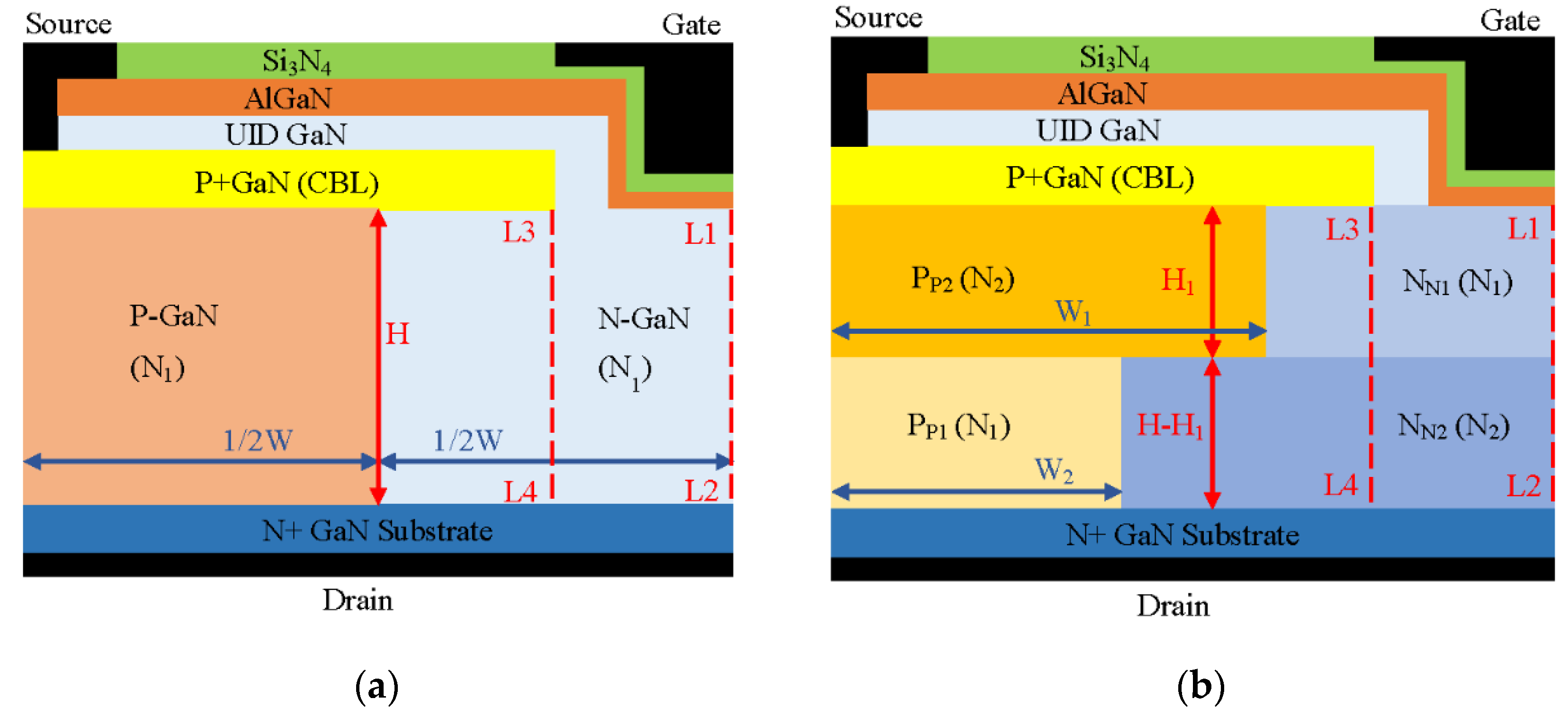
The half-cell schematic cross-section of a GaN-based trench CAVET with stepped doping microstructure (SDS-Trench CAVET) is illustrated in Figure 1b. In addition, a superjunction GaN-based trench CAVET (SJ-Trench CAVET) is also exhibited in Figure 1a for comparison. With an overall width of 5 μm, the main parameters include a 2 μm thick GaN n+ substrate, a 15 μm thick n-GaN drift layer and a 700 nm thick p+ GaN current blocking layer (CBL). The channel layer is composed of 20 nm thick Al0.25Ga0.75N and 210 nm thick UID GaN. In addition, 60 nm thick silicon nitride (Si3N4) serves as a gate dielectric. The gate length, trench depth and CBL length are set as 2 μm, 1 μm and 4 μm, respectively. The n+ GaN substrate is heavily doped with Si, and the p+ GaN is heavily doped with Mg. On the basis of Ref. [19], the origin CAVET is redesigned, and the other detailed device parameters are represented in Table 1.
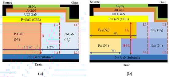
Figure 1.
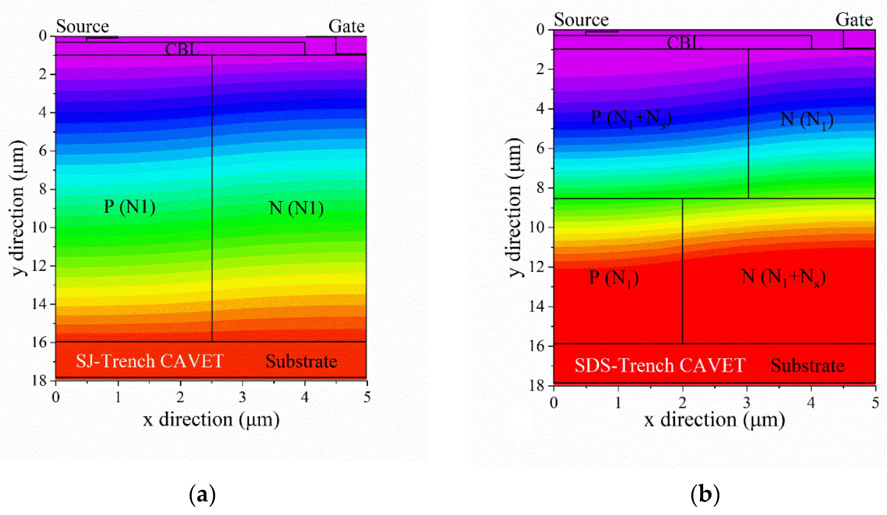
Schematic diagrams of (a) SJ-Trench CAVET and (b) SDS-Trench CAVET. Lines L1L2 and L3L4 indicate the vertical path along device center and CBL, respectively.

Table 1.
Key device parameters set in simulation [19].
As is shown in Figure 1a, half of the GaN drift layer in the SJ-Trench CAVET is divided into an n-pillar and a p-pillar with the same width (1/2W) and the same height (H). In the SDS-Trench CAVET, the GaN drift layer is evenly separated into a top stepped doping microstructure and a bottom stepped doping microstructure. In addition, both the top part and bottom part of the stepped doping microstructure are divided into two parts, the p-doping area below the CBL and the n-doping area adjacent to it. The same doping concentration (N1) is used in both top n-doping part NN1 and bottom p-doping part PP1. Simultaneously, the same doping concentration (N2) is used in both bottom n-doping part NN2 and top p-doping part PP2. Doping concentration increment Ns is defined as N2 minus N1. In addition, doping concentration N1 in the SDS-Trench CAVET is initially set equal to that of the n- and p-pillars in the SJ-Trench CAVET. For simplicity, typical N1 concentrations, namely, from 0.5 × 1016 cm−3 to 2 × 1016 cm−3, are utilized in simulations. Top part NN1 and bottom part PP1 keep the same width (W2); thus, bottom part NN2 and top part PP2 are given the same width (W1). It is worth noting that W1 should not exceed the length of the CBL to avoid excessive depletion of 2DEG in the channel.
To obtain more accurate results in Silvaco TCAD, the concentration dependent (CONSRH) and Auger physical models are used as recombination models, while Selberherr’s Model (IMPACT SELB) is adopted for impact ionization. In addition, the high-field-saturation and -polarization models are also used in the simulation. According to Ref. [10], Li et al. proposed and simulated a classic GaN vertical superjunction HEMT. Thus, the model and material parameters could refer to a similar device. The parameter details of low-field-mobility models and Farahmand-Modified Caughey–Thomas (FMCT) models are listed in Table 2.
Table 2.
Material parameters used in simulation.
When the breakdown performance is simulated, the avalanche model with a dependent electric field is adopted in the simulations. The impact-ionization rate is defined by [20]:
In Equation (1), and refer to the concentrations of electrons and holes, respectively, while and refer to the saturation velocities of electrons and holes, respectively, where and are the values of the impact-ionization coefficient related to the electric field. Equations (2) and (3) define and as follows:
In Equations (2) and (3) the temperature dependence of the phonon gas against which carriers are accelerated is expressed by parameters and . Coefficients , , and are fitting parameters, with modeling parameters = 2.81 × 108 cm−1, = 3.43 × 10⁷ V/cm, = 5.41 × 106 cm−1 and = 1.96 × 10⁷ V/cm [21].
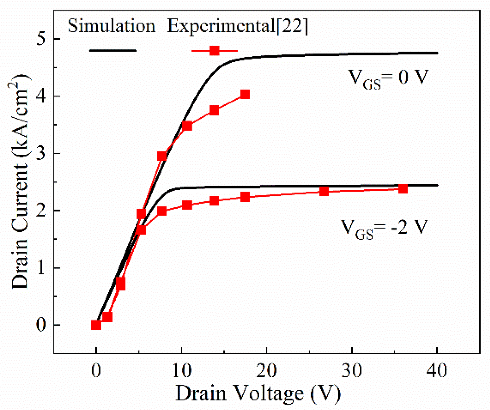
In order to examine the validity of the proposed model and parameters, Figure 2 compares the experimental results from Chowdhury [22] et al. and the simulation results when the normally on CAVET is in the on state at VGS = 0, −2 V. The reference is similar to the designed CAVET; thus, these models are considered available in simulations. As shown in Figure 2, the IDS–VDS curve shows a great fit between the experimental data and the simulation results. In addition, Ron,sp also obviously indicates a good agreement between them. Thus, the models adopted are proved to be effective and correct.
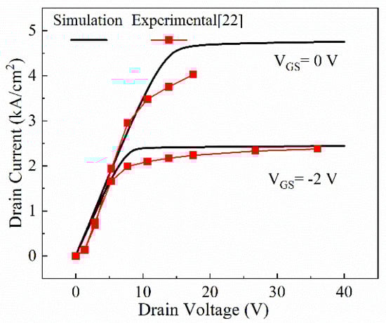
Figure 2.
Experimental- [22] and numerical-result comparison of on-state I–V characteristics.
3. Results and Discussion
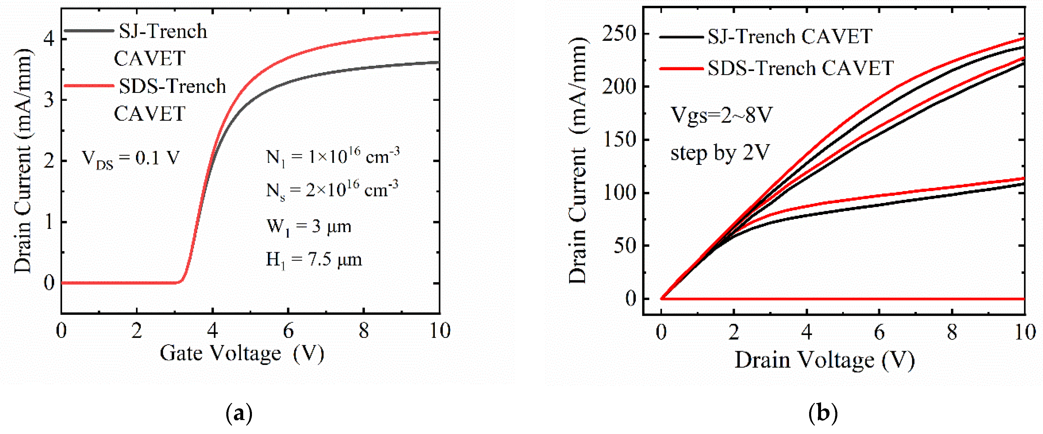
Figure 3 juxtaposes the transfer characteristics of the two devices with their output characteristics. In Figure 3a, the same threshold voltage (Vth) of 3.1 V is manifested in the SDS-Trench CAVET and SJ-Trench CAVET. However, compared with the SJ-Trench CAVET, the drain current of the SDS-Trench CAVET prevails when the gate voltage goes beyond Vth, which indicates a smaller resistance in the proposed structure. Furthermore, in Figure 3b, the noticeable enhancement of the on-state I–V curve demonstrates that the Ron,sp value of 2.08 mΩ·cm2 in the SDS-Trench CAVET is smaller than that of 2.37 mΩ·cm2 in the SJ-Trench CAVET.
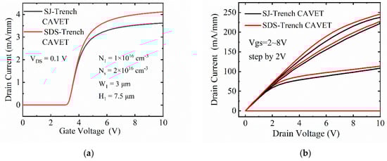
Figure 3.
Comparison of on-state I–V characteristics for two structures, including (a) transfer curves and (b) output curves.
To explain the upgraded performance of the SDS-Trench CAVET, the on-state current-density distributions are analyzed in Figure 4. For both devices, only the n-doping area in the drift is conductive, since n+ substrate/p-GaN is under reversed bias as well as lateral n/p connection [10,23]. As shown in Figure 3b,c, the horizontal current paths are exhibited in the SDS-Trench CAVET and SJ-Trench CAVET. Obviously, in the SDS-Trench CAVET, NN1 owns a narrower current path, but NN2 holds a wider current path, owing to the varied width of the stepped doping part. However, the current density in NN1 is greater than that in the corresponding position in the SJ-Trench CAVET, which is attributed to the extended PP1 with a higher doping concentration, making the electric charge accumulate in NN1. From Figure 4a, a greater current density along line L1L2 can be seen in the n-doping area of the SDS-Trench CAVET. It can be noticed that the current-density curve in NN2 is slightly lower than that in the corresponding position in the SJ-Trench CAVET. As for the reason, the higher doping concentration in NN2 may bring higher current density, but the electrons disperse in the wider N GaN drift. Consequently, with a spacious current direction and a high current density, the proposed device represents the potential to modulate current density and promote current conduction.
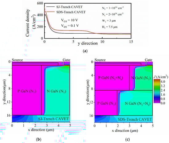
Figure 4.
(a) On-state current-density curve of two devices along line L1L2 and (b,c) corresponding total two-dimensional distribution for SJ-Trench CAVET and SDS-Trench CAVET under the conditions of VGS = 10 V and VDS = 0.1 V (in log scale).
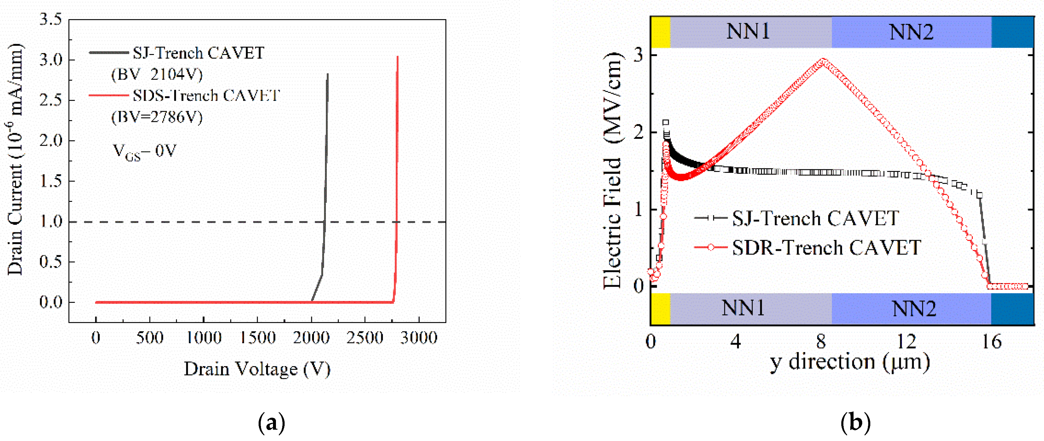
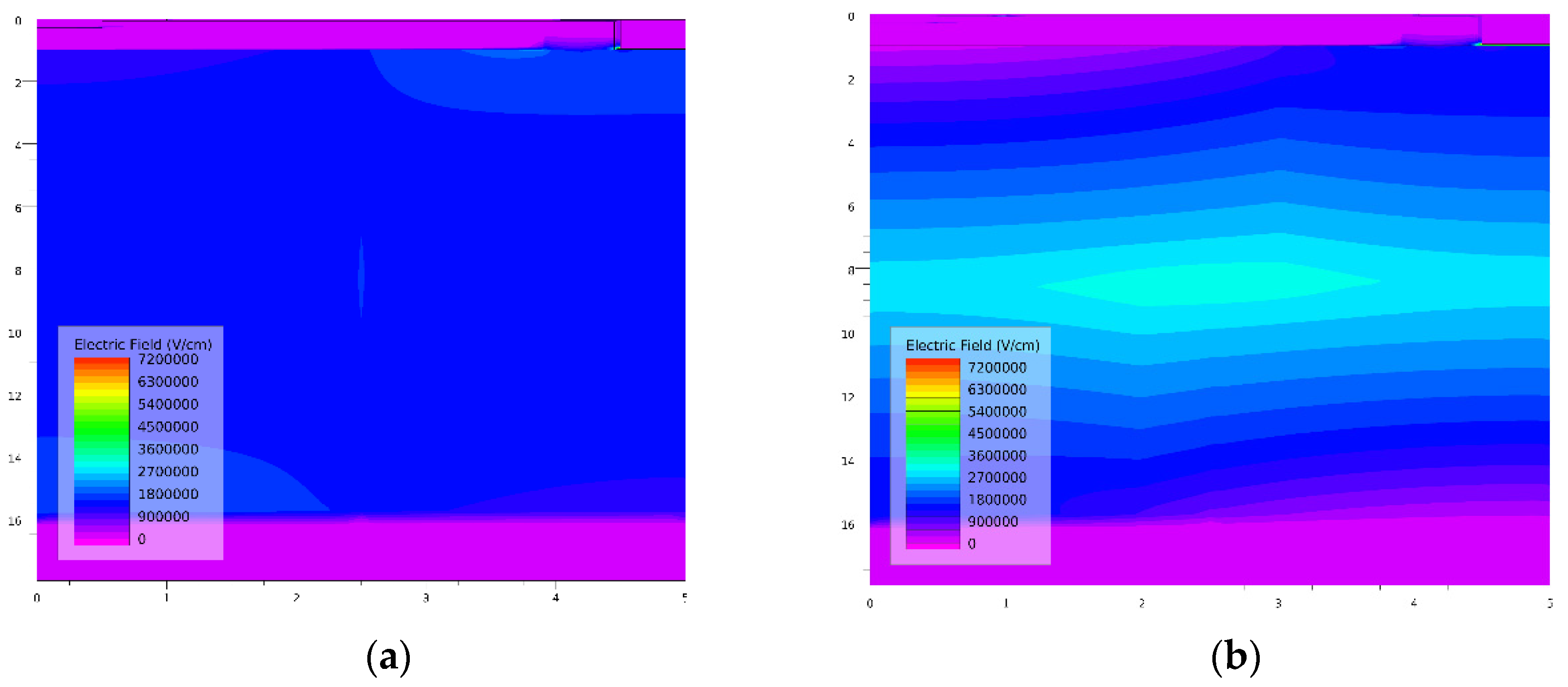
From the corresponding off-state breakdown characteristics in Figure 5a, the BVs of the SJ-Trench CAVET and SDS-Trench CAVET extracted at ID = 1 × 10⁻⁶ mA/mm are 2104 V and 2786 V, respectively. To investigate the distinction between the two devices and mechanisms accounting for it, the electric field and the corresponding contour plots are illustrated in Figure 5b and Figure 6, respectively. Figure 5b represents the comparison of the electric-field strengths along line L3L4 in the proposed structures. As can be seen, owing to the incomplete depleted 2DEG in the trench, there are two small peaks of electric field in the corresponding position. However, the larger p-GaN region below the CBL in the SDS-Trench CAVET consumes more electric field in the trench corner, resulting in a lower peak at the CBL/GaN drift interface. Additionally, since NN2 is given a higher doping concentration and a larger region, the electric-field strength is enhanced and reaches its maximum at the dividing line. In addition, the electric-field strength approaching the substrate is smaller in the SDS-Trench CAVET, which could be explained by the fact that the electric field is distributed and weakened in the larger NN2. The greater value of the electric field in the SDS-Trench CAVET results in the tolerance to higher forward voltage [24]. Figure 6 plots more details about the two peaks and the whole distribution in the GaN drift. In the SJ-CAVET, there are only two strong electric fields, which are located in the trench corner and substrate. However, the drift layer in the SDS-CAVET is much brighter than the former, especially at the stepped doping interface. Such a great electric-field strength guarantees the high current levels and high voltage tolerance of the device.
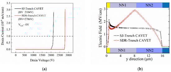
Figure 5.
(a) Off-state BV curves of SJ-Trench CAVET and SDS-Trench CAVET and (b) electric-field strength comparison in the GaN drift along line L3L4.
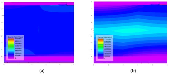
Figure 6.
Corresponding entire-electric-field contour plots of (a) SJ-CAVET and (b) SDS-CAVET
In Figure 7, the off-state potential equipotential lines show similar slopes in the SJ-Trench CAVET and SDS-Trench CAVET, which guarantee device stability in breakdown performance. Compared with the SJ-Trench CAVET, in the SDS-Trench CAVET, the low-potential areas below the CBL move down slightly, and the high-potential areas above the substrate move upward a lot, causing narrower medium-potential areas. The variation in equipotential-line densities verifies the electric-field-distribution result in Figure 5, whereby the electric-field strength near the middle is enhanced, while that near the bottom is degraded in n- and p-pillars. The total enlarged high-potential distribution in the bottom area is beneficial for breakdown performance, especially during reverse blocking.

Figure 7.
Off-state performance of (a) SJ-Trench CAVET compared with (b) SDS-Trench CAVET according to potential equipotential surface.
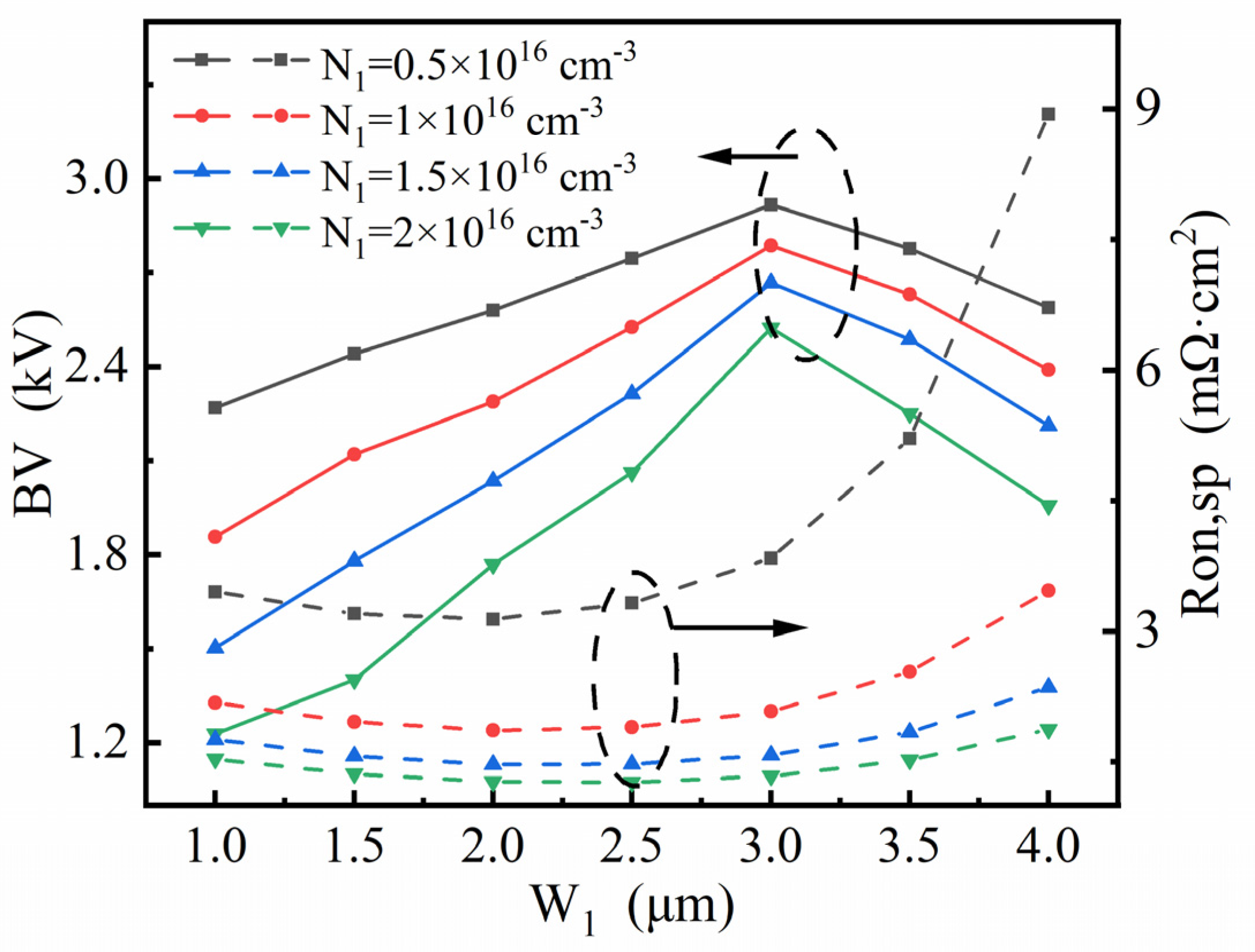
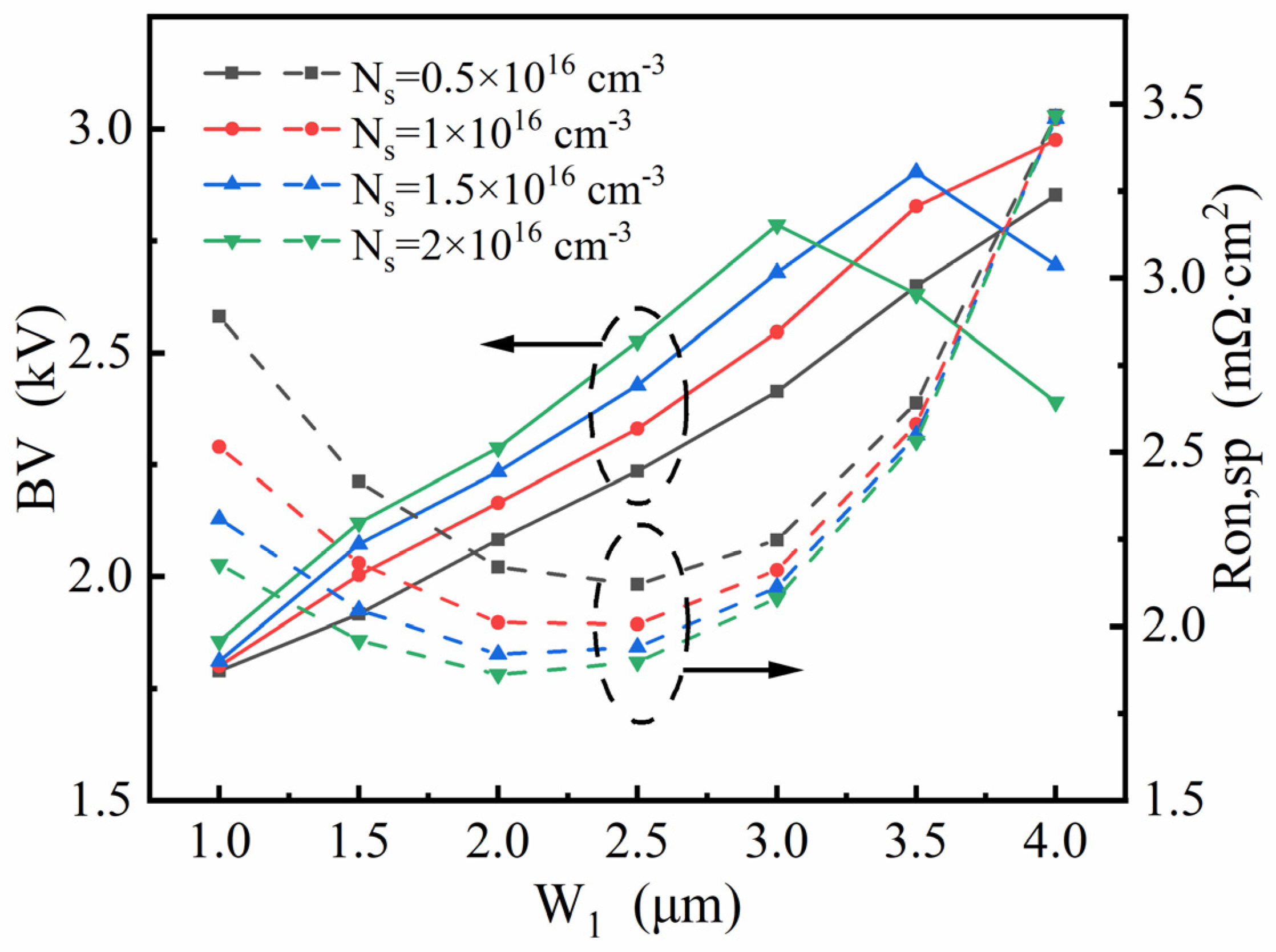
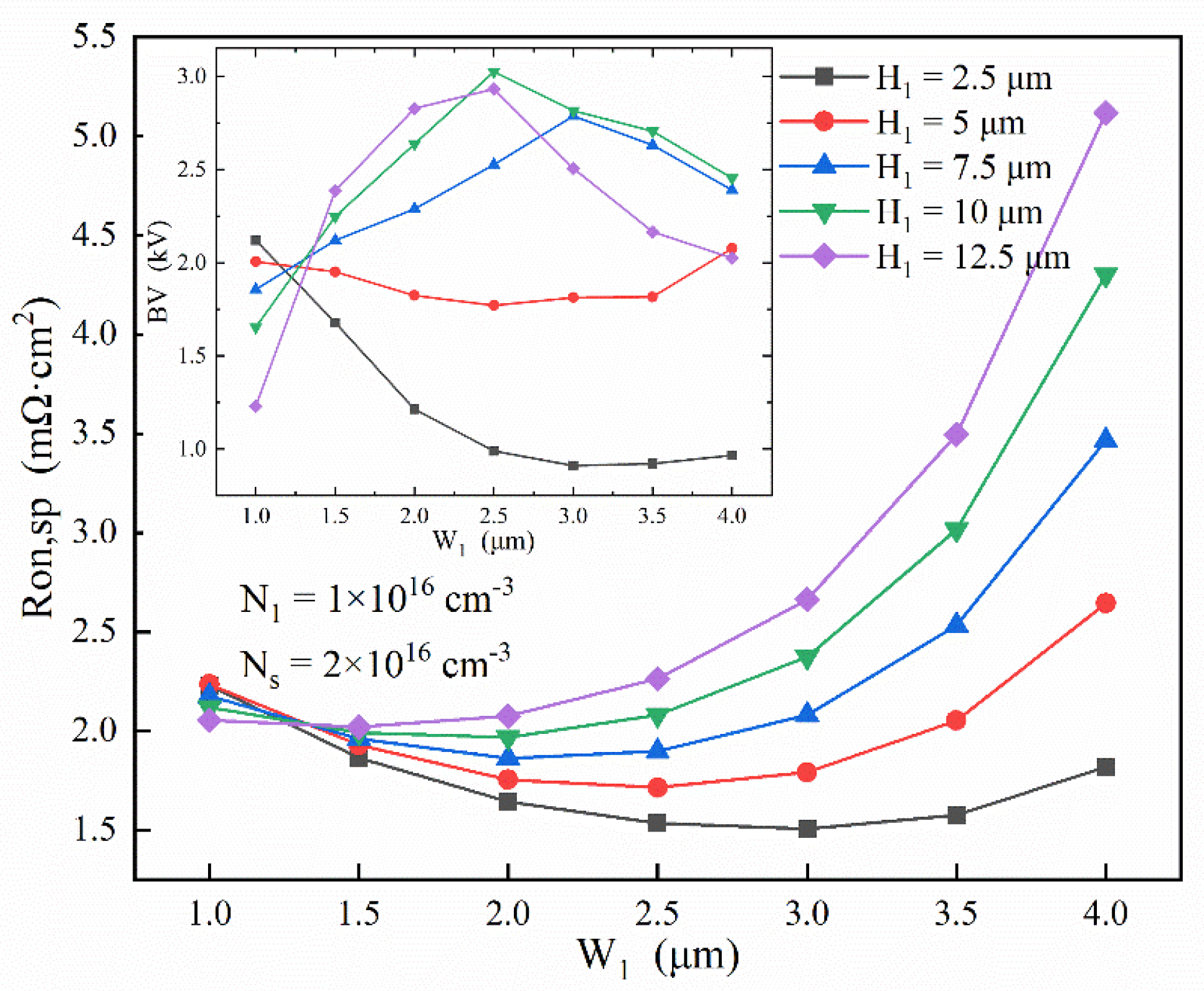
Figure 8, Figure 9 and Figure 10 show how the four key parameters, N1, Ns, H1 and W1, influence the breakdown characteristics and Ron,sp. Since the stepped doping region is composed of top part and bottom parts, step lengths W1 and W2 deserve investigation to explore their modulation effect and are consequently selected as the main variations in the optimization. Figure 8 shows the plots of the breakdown voltage and specific on-resistance versus length W1 for different values of N1 for given Ns and H1 in the SDS-Trench CAVET. As shown, Ron,sp is at its minimum when W1 is 2.0 μm or 2.5 μm, while the maximum BV appears when W1 is 3 μm. Although the largest BV is obtained with N1 = 0.5×1016 cm−3, its Ron,sp exceeds the original Ron,sp in the SJ-Trench CAVET. Thus, the best BV result, 2786 V, is obtained with N1 = 1 × 1016 cm−3 with a slightly reduced Ron,sp of 2.08 mΩ·cm2, or a lower Ron,sp of 1.34 mΩ·cm2 and a relatively high BV of 2500 V could be acquired when N1 = 2 × 1016 cm−3. The above two trade-offs are both represented with W1 = 3 μm, which means that such a stepped doping method is effective and significant in enhancing the performance of the devices.
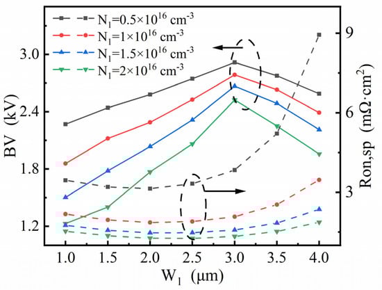
Figure 8.
Investigation of W1 affecting optimized BV and Ron,sp in SDS-Trench CAVET for varied values of N1 for a given Ns = 2 × 1016 cm−3.
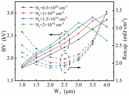
Figure 9.
Investigation of W1 affecting optimized BV and Ron,sp in SDS-Trench CAVET for varied values of Ns for a given N1 = 1 × 1016 cm−3.
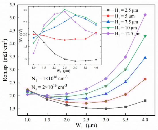
Figure 10.
Investigation of H1 and W1 affecting optimized BV and Ron,sp in SDS-Trench CAVET for varied values of N1 for given Ns = 2 × 1016 cm−3 and N1 = 1 × 1016 cm−3.
In Figure 9, for given N1 and H1, the different values of Ns are investigated to further examine the above results. The peak of the BV emerges when W1 is 3 μm or longer. While the BV increases as Ns declines, the rapidly enlarged Ron,sp cannot be ignored. Therefore, the optimized result is achieved with Ns = 2 × 1016 cm−3, since it represents a higher BV and lower Ron,sp than other Ns, especially when W1 is smaller than 3 μm.
Based on the above results, Figure 10 explores how the thickness of the stepped doping structure affects the performance of the SDS-Trench CAVET with given Ns = 2 × 1016 cm−3 and N1 = 1 × 1016 cm−3. It seems that Ron,sp follows a regular pattern, whereby as W1 is expanded, Ron,sp first decreases and then increases. In addition, when H1 is enlarged, Ron,sp rapidly declines, which could be ascribed to the overconsumption of 2DEG by the broadened p-doping region. However, in the embedded figure of BV variation, the trend is not the same as that of Ron,sp. As is shown, when W1 is extended, the BV first increases and then drops when H1 is larger than 5 μm, while the BV seldom changes or even descends when H1 is smaller than 5 μm. Pursuing the highest BV, 10 μm H1 provides a 3024 V breakdown voltage with a non-deteriorated Ron,sp of 2.08 mΩ·cm2, which is obtained when W1 = 2.5 μm. Such a high breakdown voltage could be attributed to the thickened p-doping region beneath the CBL, greatly affecting the reverse-blocking process [25].
4. Fabrication Process
Recent years witnessed more and more mature GaN-growth technologies, such as technologies for thick in situ doping-GaN-layer growth, GaN-based selective-area-growth technologies (SAG) and GaN etching technologies. The height of the GaN drift layer grown via SAG and the depth of the plasma-etched GaN trench were reported to be more than 10 μm [26]. Therefore, the fabrication of the proposed GaN-based trench CAVET with a stepped doping microstructure is achievable, since the n-doping region and p-doping region could alternately be grown using the above technologies.
The diagrams in Figure 11 and the following procedures demonstrate an available process to realize the proposed SDS-Trench CAVET. Firstly, a p-GaN layer with doping concentration N1 and height H minus H1 is epitaxially grown via metal–organic chemical vapor deposition (MOCVD) on a bulk conductive GaN substrate. Mg ions could be implanted into the bottom p-GaN layer at 80 keV [22]. Utilizing the Cl-based inductively coupled plasma (ICP) etching process, trench 1 with width 2W1 and height H–H1 is formed. Then, the rest of the p-GaN layer is masked and an n-GaN layer with doping concentration N2 and height H–H1 is regrown via SAG in trench 1. Secondly, a p-GaN layer with doping concentration N2 and height H1 is epitaxially deposited via MOCVD. The same Mg ion-implantation method is applied to it. Simultaneously, trench 2 is etched via ICP, and the n-GaN layer with doping concentration N1 and height H1 is regrown via SAG to fill trench 2. Thirdly, a heavily Mg-implanted doped p-GaN layer is epitaxially grown via MOCVD to form a CBL layer. The current aperture is protected using an implantation mask consisting of Ti/Ni on SiO2 deposited via PECVD. The implantation mask is later removed with the wet-etching technique using hydrofluoric acid. After wet etching and MOCVD growth on the CBL layer, the final main procedures involve the deposition of the UID-GaN channel and MIS trench-gate structure. After p+GaN activation and HF surface treatment, unintentionally doped (UID) GaN is regrown on the CBL via MOCVD. Using Cl2/BCl3 gases in reactive-ion etching (RIE) to etch the trench, UV–ozone and HF cleaning treatments are performed after trench formation [12]. Subsequently, the AlGaN layers are grown via MOCVD at a high temperature. The Si3N4 dielectric is deposited on the AlGaN barrier layer via PECVD. Then, the trench gate and source are formed via ICP etching, followed by surface treatment. Next, the buried p-GaN and CBL are processed via thermal annealing with the diffusion of hydrogen and Mg activation. Later, the dielectric gate is patterned via ALD. Finally, the Ni/Au stack is taken as the gate, while the Ti/Al stack is used to form the source and backside drains, after which the entire proposed device is obtained.
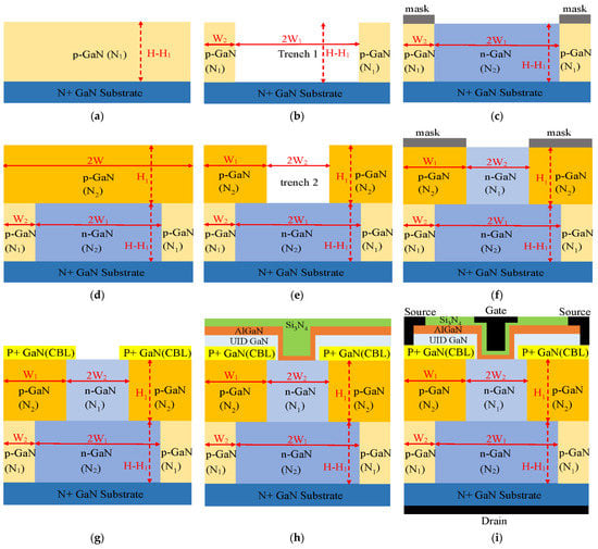
Figure 11.
A feasible process to realize the proposed SDS-Trench CAVET, showing (a) bottom-p-GaN-layer growth, (b) trench 1 etching, (c) bottom-n-GaN-layer regrowth in trench 1, (d) top-p-GaN-layer growth, (e) trench 2 etching, (f) top-n-GaN-layer regrowth in trench 2, (g) CBL-layer growth and etching, (h) UID-GaN/AlGaN/Si3N4 triple-trench-layer regrowth and (i) selective etching to form electrode and complete fabrication.
5. Conclusions
A GaN-based trench CAVET with a stepped doping microstructure is demonstrated and evaluated using two-dimensional simulations to promote the BV and Ron,sp. By modulating the step width, thickness, doping concentration and variation in the GaN drift layer, the structure presents an extremely high BV of 3024 V with Ron,sp of 2.08 mΩ·cm2. Defining Baliga’s figure of merit (FOM) as BV2/Ron,sp, the optimized device achieves a high FOM of 4.396 GW·cm−2, or the device can manifest an extremely low Ron,sp of 1.34 mΩ·cm2 with a BV of 2523 V, yielding a remarkable FOM of 4.767 GW·cm−2. The above two trade-offs exhibit the potential and superiority of the stepped doping microstructure in enhancing the performance of high-power GaN devices and applications.
Author Contributions
Conceptualization, investigation and simulation, writing—original draft preparation, Y.L.; supervision, writing—review and editing, L.X.; funding acquisition, Z.G.; validation, H.S. All authors have read and agreed to the published version of the manuscript.
Funding
This research study was funded by Key-Area Research and Development Program of Guangdong Province (2019B010128002, 2020B010171002), Guangzhou Liwan District Science and technology planning project under Grant 202004008, and Foshan Science and Technology Bureau under project No. 1920001000724.
Conflicts of Interest
The authors declare no conflict of interest.
References
- Xiao, M.; Ma, Y.; Liu, K.; Cheng, K.; Zhang, Y. 10 kV, 39 mΩ·cm2 multi-channel AlGaN/GaN schottky barrier diodes. IEEE Electron Device Lett. 2021, 42, 808–811. [Google Scholar] [CrossRef]
- Sung, J.; Park, S.; So, H. Cube-shaped GaN UV photodetectors using 3D-printed panels for omnidirectional detection. IEEE Sens. J. 2021, 21, 16403–16408. [Google Scholar] [CrossRef]
- Pengelly, R.S.; Wood, S.M.; Milligan, J.W.; Sheppard, S.T.; Pribble, W.L. A review of GaN on SiC high electron-mobility power transistors and MMICs. IEEE Trans. Microw. Theory Tech. 2012, 60, 1764–1783. [Google Scholar] [CrossRef]
- Huang, H.; Liang, Y.C.; Samudra, G.S.; Chang, T.-F.; Huang, C.-F. Effects of gate field plates on the surface state related current collapse in AlGaN/GaN HEMTs. IEEE Trans. Power Electron 2014, 29, 2164–2173. [Google Scholar] [CrossRef]
- Mao, W.; Fan, J.-S.; Du, M.; Zhang, J.-F.; Zheng, X.-F.; Wang, C.; Ma, X.-H.; Zhang, J.-C.; Hao, Y. Analysis of the modulation mechanisms of the electric field and breakdown performance in AlGaN/GaN HEMT with a T-shaped field-plate. Chin. Phys. B 2016, 25, 430–434. [Google Scholar] [CrossRef]
- Heidel, T.D.; Gradzki, P. Power devices on bulk gallium nitride substrates: An overview of ARPA-E’s SWITCHES program. In Proceedings of the IEEE International Electron Devices Meeting, San Francisco, CA, USA, 15–17 December 2014. [Google Scholar]
- Fu, H.; Fu, K.; Chowdhury, S.; Palacios, T.; Zhao, Y. Vertical GaN power devices: Device principles and fabrication technologies—Part I. IEEE Trans. Electron Devices. 2021, 68, 3200–3211. [Google Scholar] [CrossRef]
- Li, W.; Chowdhury, S. Design and fabrication of a 1.2kV GaN-based MOS vertical transistor for single chip normally off operation. Phys. Status Solidi A Appl. Mat. 2016, 213, 2714–2720. [Google Scholar] [CrossRef]
- Gupta, C.; Chan, S.H.; Enatsu, Y.; Agarwal, A.; Keller, S.; Mishra, U.K. OG-FET: An in-situ oxide, GaN interlayer-based vertical trench MOSFET. IEEE Electron Device Lett. 2016, 37, 1601–1604. [Google Scholar] [CrossRef]
- Li, Z.; Chow, T.P. Design and Simulation of 5-20-kV GaN Enhancement-Mode Vertical Superjunction HEMT. IEEE Trans. Electron Devices. 2013, 60, 3230–3237. [Google Scholar] [CrossRef]
- Shibata, D.; Kajitani, R.; Ogawa, M.; Tanaka, K.; Tamura, S.; Hatsuda, T.; Ishida, M.; Ueda, T. 1. In 7 kV/1.0 mΩ cm2 normally-off vertical GaN transistor on GaN substrate with regrown p-GaN/AlGaN/GaN semipolar gate structure. In Proceedings of the 2016 IEEE International Electron Devices Meeting (IEDM), San Francisco, CA, USA, 3–7 December 2016. [Google Scholar]
- Ji, D.; Agarwal, A.; Li, H.; Li, W.; Keller, S.; Chowdhury, S. 880V/2.7 mΩ·cm2 MIS gate trench CAVET on bulk GaN substrates. IEEE Electron Device Lett. 2018, 39, 863–865. [Google Scholar] [CrossRef]
- Bai, P.; Zhou, Q.; Huang, P.; Chen, K.; Zhu, L.; Wang, S.; Gao, W.; Zhou, C.; Zhang, B. A novel trench-gated vertical GaN transistor with dual-current-aperture by electric-field engineering for high breakdown voltage. IEEE Trans. Electron Devices. 2022, 69, 1219–1225. [Google Scholar] [CrossRef]
- Deboy, G.; Marz, N.; Stengl, J.-P.; Strack, H.; Tihanyi, J.; Weber, H. A new generation of high voltage MOSFETs breaks the limit line of silicon. In Proceedings of the International Electron Devices Meeting 1998. Technical Digest (Cat. No. 98CH36217), San Francisco, CA, USA, 6–9 December 1998. [Google Scholar]
- Chen, J.; Sun, W.; Zhang, L.; Zhu, J.; Lin, Y. A review of superjunction vertical diffused MOSFET. IETE Tech. Rev. 2012, 29, 44–52. [Google Scholar] [CrossRef]
- Luo, X.; Wang, Y.; Cao, F.; Yu, C.-H.; Fei, X.-X. A breakdown enhanced AlGaN/GaN MISFET with source-connected P-buried layer. Superlattices Microstruct. 2017, 112, 517–527. [Google Scholar] [CrossRef]
- Zhu, C.; Zhou, X.; Feng, Z.; Zhao, Z.; Wei, Z.; Zhao, Z. Theoretical investigation of high-voltage superjunction GaN-based vertical heterojunction field effect transistor with ununiformly doped buffer to suppress charge imbalance effect. Semicond. Sci. Technol. 2019, 34, 065012. [Google Scholar] [CrossRef]
- Zhang, M.; Guo, Z.; Huang, Y.; Li, Y.; Ma, J.; Xia, X.; Tan, X.; Xia, F.; Sun, H. Study of AlGaN/GaN vertical superjunction HEMT for improvement of breakdown voltage and specific on-resistance. IEEE Access. 2021, 9, 9895–9902. [Google Scholar] [CrossRef]
- Zhang, X.; Chen, X.; Li, W.; Wang, L.; Tao, L.; Li, X. Simulation study of GaN-based Trench CAVET with p-shielded region. In Proceedings of the 21st International Conference on Electronic Packaging Technology (ICEPT), Guangzhou, China, 12–15 August 2020. [Google Scholar]
- Wang, Y.; Bao, M.-T.; Cao, F.; Tang, J.-X.; Luo, X. Technology computer aided design study of GaN MISFET with double p-buried layers. A breakdown enhanced AlGaN/GaN MISFET with source-connected P-buried layer. IEEE Access. 2019, 7, 87574–87581. [Google Scholar] [CrossRef]
- Oguzman, I.H.; Bellotti, E.; Brennan, K.F.; Kolnik, J.; Wang, R.; Ruden, P.P. Theory of hole initiated impact ionization in bulk zincblende and wurtzite GaN. J. Appl. Phys. 1997, 81, 7827–7834. [Google Scholar] [CrossRef]
- Chowdhury, S.; Wong, M.H.; Swenson, B.L.; Mishra, U.K. CAVET on bulk GaN substrates achieved with MBE-regrown AlGaN/GaN layers to suppress dispersion. IEEE Electron Device Lett. 2012, 33, 41–43. [Google Scholar] [CrossRef]
- Ji, D.; Laurent, M.A.; Agarwal, A.; Li, W.; Mandal, S.; Keller, S.; Chowdhury, S. Normally OFF trench CAVET with active mg-doped GaN as current blocking layer. IEEE Trans. Electron Devices. 2017, 64, 805–808. [Google Scholar] [CrossRef]
- Yin, R.; Li, Y.; Wen, C.P.; Fu, Y.; Hao, Y.; Wang, M.; Shen, B. High Voltage Vertical GaN-on-GaN Schottky Barrier Diode with High Energy Fluorine Ion Implantation Based on Space Charge Induced Field Modulation (SCIFM) Effect. In Proceedings of the 32nd International Symposium on Power Semiconductor Devices and ICs (ISPSD), Vienna, Austria, 13–18 September 2020. [Google Scholar]
- Abhinay, S.; Arulkumaran, S.; Ng, G.L.; Ranjan, K.; Deki, M.; Nitta, S.; Honda, Y.; Amano, H. Effects of drift layer thicknesses in reverse conduction mechanism on vertical GaN-on-GaN SBDs grown by MOCVD. In Proceedings of the 2019 Electron Devices Technology and Manufacturing Conference (EDTM), Singapore, 12–15 March 2019. [Google Scholar]
- Harrison, S.E.; Voss, L.F.; Torres, A.M.; Frye, C.D.; Shao, Q.; Nikolic, R.J. Ultradeep electron cyclotron resonance plasma etching of GaN. J. Vac. Sci. Technol. 2017, 35, 061303. [Google Scholar] [CrossRef]


Publisher’s Note: MDPI stays neutral with regard to jurisdictional claims in published maps and institutional affiliations. |
© 2022 by the authors. Licensee MDPI, Basel, Switzerland. This article is an open access article distributed under the terms and conditions of the Creative Commons Attribution (CC BY) license (https://creativecommons.org/licenses/by/4.0/).