
SAW Resonators and Filters Based on Sc0.43Al0.57N on Single Crystal and Polycrystalline Diamond

 , , and
Abstract
:1. Introduction
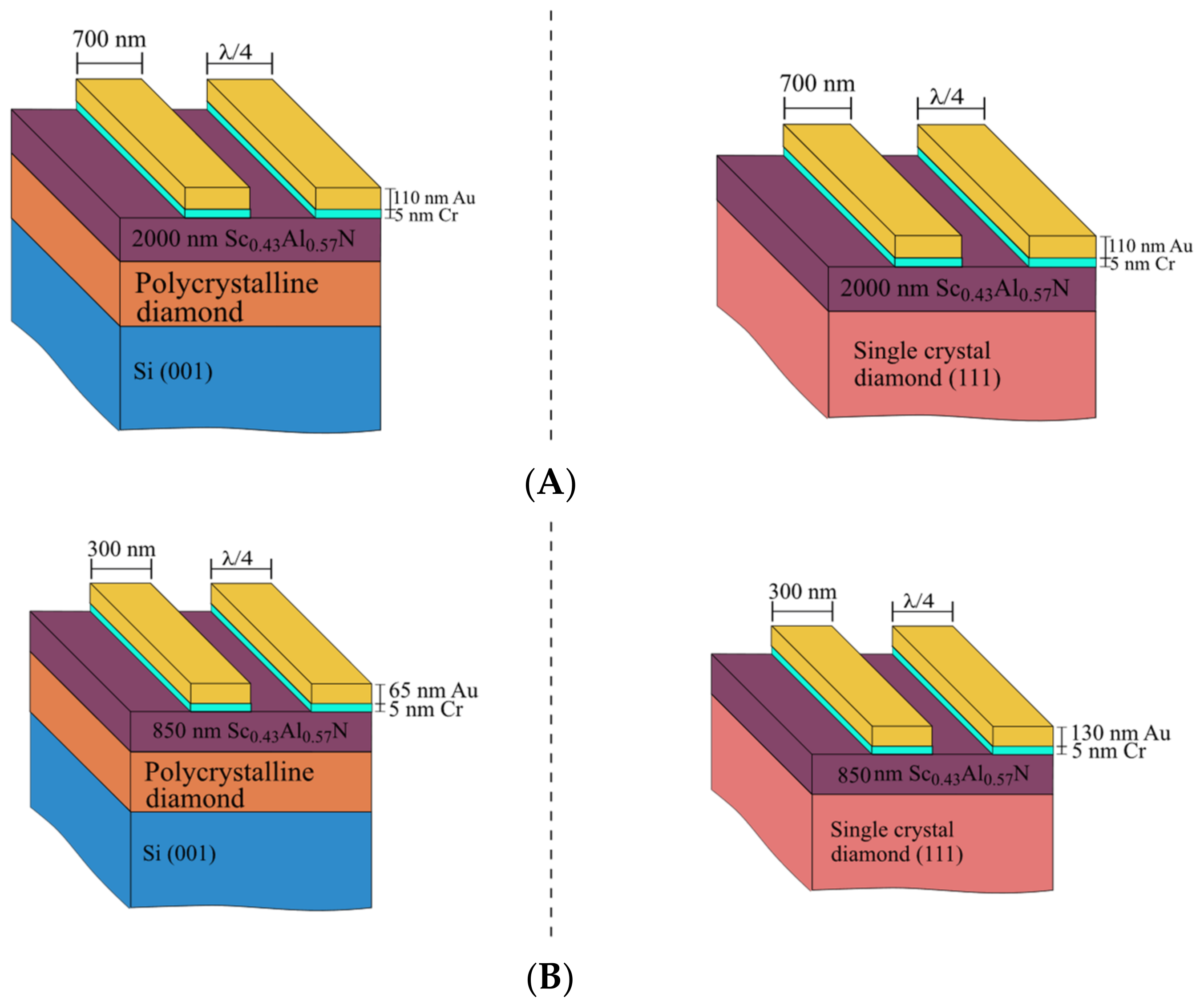
2. Materials and Methods
3. Results
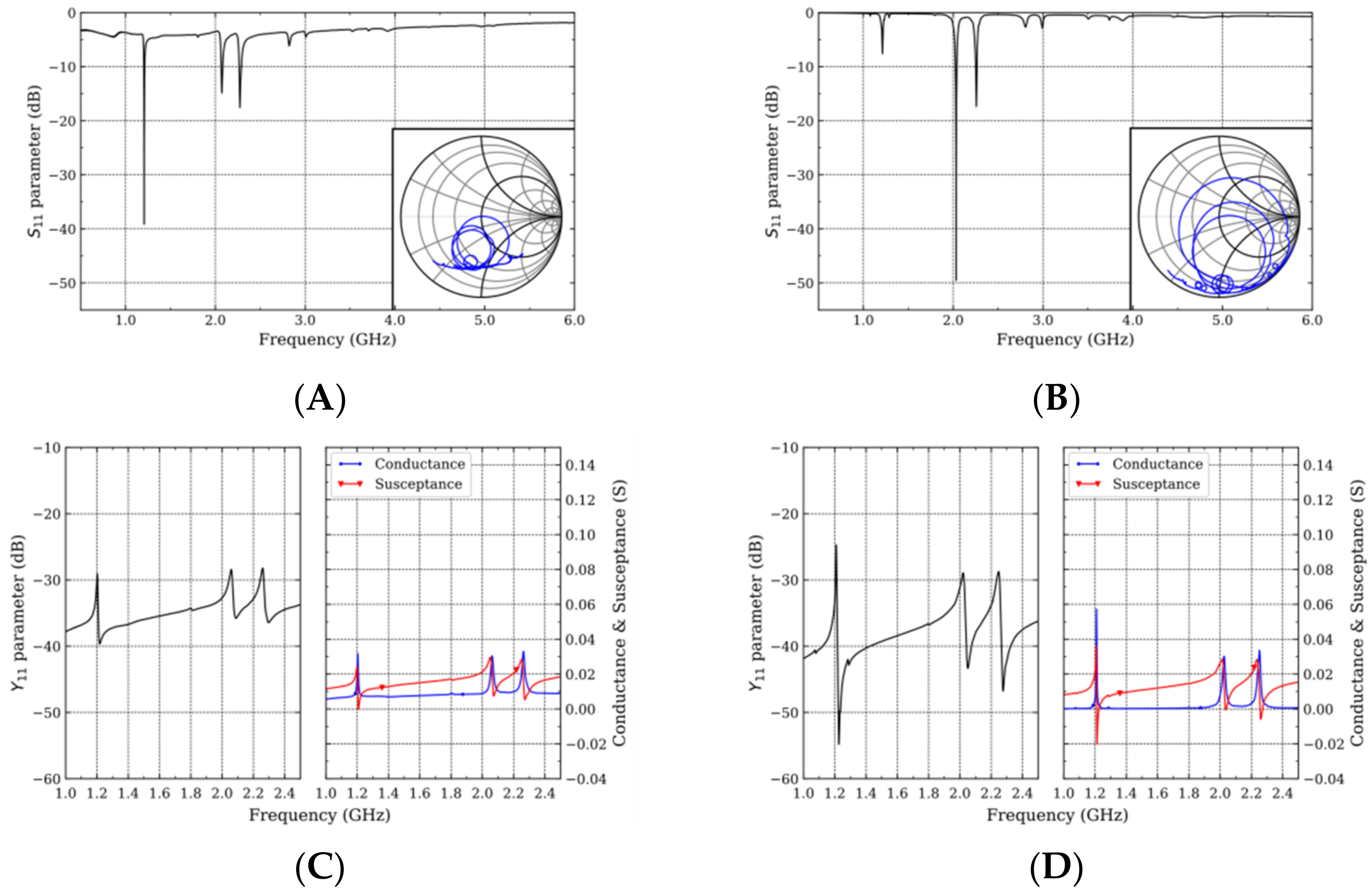
3.1. Resonators
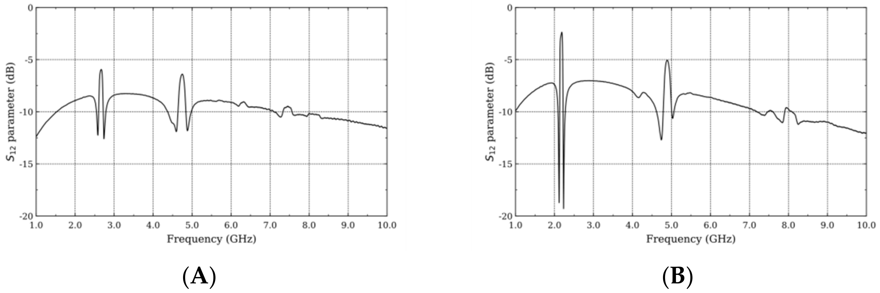
3.2. Filters
4. Discussion

| ScAlN Composition | Synthesis Technique | Target | Substrate | Resonance Frequency (GHz) | Electrode Metal | Q | |
|---|---|---|---|---|---|---|---|
| [29] | MBE | - | Si | 3.6 | Ti/Au | 3.7 | 146 |
| [17] | RF | PCD | 2.5−3.5 | Al/Cr | 5.5–4.5 | 396–227 | |
| [30] | DC | ScAlN alloy | Si | 0.2–0.3 | Ti/Au | 2 | 100 |
| [33] | Pulsed DC | Si | R 1.4 | Pt | 0.5 | 140 | |
| [18] | Pulsed DC | PCD | R 1.5–S 2.6 | Pt | 2.8 | R167–S180 | |
| [34] | RF | Dual | SCD SCD | 3.75 2.9 | Cu Cu | 6.1 3.8 | 520 - |
| [32] | Pulsed DC | Dual (Al + Sc targets) | Sapphire | 1.9–1.7 | Pt | 1.3–2.4 | 659–538 |
| This work | Pulsed DC | PCD&SCD | R 1.2–S 2.03 | Cr/Au | 3.2–3.7 | R 250–S ~50 |
5. Conclusions
Supplementary Materials
Author Contributions
Funding
Conflicts of Interest
References
- Farnell, G.; Adler, E. Elastic Wave Propagation in Thin Layers. In Physical Acoustics; Academic Press: New York, NY, USA, 1972; Volume 9, pp. 35–127. [Google Scholar] [CrossRef]
- Campbell, C.; Burgess, J.C. Surface Acoustic Wave Devices and Their Signal Processing Applications. J. Acoust. Soc. Am. 1991, 89, 1479–1480. [Google Scholar] [CrossRef]
- Morgan, D.P. History of SAW devices. In Proceedings of the 1998 IEEE International Frequency Control Symposium (Cat. No.98CH36165), Pasadena, CA, USA, 29 May 1998; pp. 439–460. [Google Scholar] [CrossRef]
- Delsing, P.; Cleland, A.N.; Schuetz, M.J.; Knörzer, J.; Giedke, G.; Cirac, J.I.; Srinivasan, K.; Wu, M.; Balram, K.C.; Bäuerle, C.; et al. The 2019 surface acoustic waves roadmap. J. Phys. D Appl. Phys. 2019, 52, 353001. [Google Scholar] [CrossRef]
- Hashimoto, K. Advances in RF SAW devices: What are demanded? In Proceedings of the 2016 European Frequency and Time Forum (EFTF), York, UK, 4–7 April 2016; pp. 1–4. [Google Scholar] [CrossRef]
- Wang, W.; Wu, H. High selectivity SAW DMS filter with in-between shorted-gratings. In Proceedings of the 2010 IEEE International Ultrasonics Symposium, San Diego, CA, USA, 11–14 October 2010; no. 10774073. pp. 1263–1266. [Google Scholar] [CrossRef]
- Ababneh, A.; Schmid, U.; Hernando, J.; Sánchez-Rojas, J.L.; Seidel, H. The influence of sputter deposition parameters on piezoelectric and mechanical properties of AlN thin films. Mater. Sci. Eng. B 2010, 172, 253–258. [Google Scholar] [CrossRef]
- Duquenne, C.; Besland, M.-P.; Tessier, P.-Y.; Gautron, E.; Scudeller, Y.; Averty, D. Thermal conductivity of aluminium nitride thin films prepared by reactive magnetron sputtering. J. Phys. D Appl. Phys. 2012, 45, 015301. [Google Scholar] [CrossRef]
- Akiyama, M.; Kamohara, T.; Kano, K.; Teshigahara, A.; Takeuchi, Y.; Kawahara, N. Enhancement of Piezoelectric Response in Scandium Aluminum Nitride Alloy Thin Films Prepared by Dual Reactive Cosputtering. Adv. Mater. 2009, 21, 593–596. [Google Scholar] [CrossRef]
- Tasnádi, F.; Alling, B.; Höglund, C.; Wingqvist, G.; Birch, J.; Hultman, L.; Abrikosov, I.A. Origin of the Anomalous Piezoelectric Response in WurtziteScxAl1−xNAlloys. Phys. Rev. Lett. 2010, 104, 137601. [Google Scholar] [CrossRef] [Green Version]
- Högund, C.; Birch, J.; Alling, B.; Bareño, J.; Czigany, Z.; Persson, P.; Wingqvist, G.; Zukauskaite, A.; Hultman, L. Wurtzite structure Sc1−xAlxN solid solution films grown by reactive magnetron sputter epitaxy: Structural characterization and first-principles calculations. J. Appl. Phys. 2010, 107, 123515. [Google Scholar] [CrossRef] [Green Version]
- Talley, K.R.; Millican, S.L.; Mangum, J.; Siol, S.; Musgrave, C.B.; Gorman, B.; Holder, A.M.; Zakutayev, A.; Brennecka, G.L. Implications of heterostructural alloying for enhanced piezoelectric performance of (Al,Sc)N. Phys. Rev. Mater. 2018, 2, 063802. [Google Scholar] [CrossRef] [Green Version]
- Caro, M.A.; Zhang, S.; Riekkinen, T.; Ylilammi, M.; Moram, A.M.; Lopez-Acevedo, O.; Molarius, J.; Laurila, T. Piezoelectric coefficients and spontaneous polarization of ScAlN. J. Phys. Condens. Matter 2015, 27, 245901. [Google Scholar] [CrossRef] [PubMed]
- Zhang, S.; Holec, D.; Fu, W.Y.; Humphreys, C.J.; Moram, M.A. Tunable optoelectronic and ferroelectric properties in Sc-based III-nitrides. J. Appl. Phys. 2013, 114, 133510. [Google Scholar] [CrossRef] [Green Version]
- Berlincourt, D.A.; Curran, D.R.; Jaffe, H. Piezoelectric and piezomagnetic materials and their function in transducers. In Physical Acoustics Principles and Methods; Mason, W.P., Ed.; Academic Press: New York, NY, USA, 1964; pp. 170–270. [Google Scholar]
- Arsenovic, A.; Hillairet, J.; Anderson, J.; Forsten, H.; Ries, V.; Eller, M.; Sauber, N.; Weikle, R.; Barnhart, W.; Forstmayr, F. scikit-rf: An Open Source Python Package for Microwave Network Creation, Analysis, and Calibration [Speaker’s Corner]. IEEE Microw. Mag. 2022, 23, 98–105. [Google Scholar] [CrossRef]
- Kobayashi, Y.; Tsuchiya, T.; Okazaki, M.; Asao, Y.; Hashimoto, K.; Shikata, S. High-frequency surface acoustic wave resonator with ScAlN/hetero-epitaxial diamond. Diam. Relat. Mater. 2021, 111, 108190. [Google Scholar] [CrossRef]
- Lozano, M.S.; Chen, Z.; Williams, O.A.; Iriarte, G.F. Giant Reflection Coefficient on Sc 0.26 Al 0.74 N Polycrystalline Diamond Surface Acoustic Wave Resonators. Phys. Status Solidi 2019, 216, 1900360. [Google Scholar] [CrossRef]
- Liu, H.; Zhang, Q.; Zhao, X.; Wang, F.; Chen, M.; Li, B.; Fu, S.; Wang, W. Highly coupled leaky surface acoustic wave on hetero acoustic layer structures based on ScAlN thin films with a c-axis tilt angle. Jpn. J. Appl. Phys. 2021, 60, 031002. [Google Scholar] [CrossRef]
- Lu, R.; Li, M.-H.; Yang, Y.; Manzaneque, T.; Gong, S. Accurate Extraction of Large Electromechanical Coupling in Piezoelectric MEMS Resonators. J. Microelectromech. Syst. 2019, 28, 209–218. [Google Scholar] [CrossRef]
- Feld, D.A.; Parker, R.; Ruby, R.; Bradley, P.; Dong, S. After 60 years: A new formula for computing quality factor is warranted. In Proceedings of the 2008 IEEE Ultrasonics Symposium, Beijing, China, 2–5 November 2008; pp. 431–436. [Google Scholar] [CrossRef]
- Ruby, R. 11E-2 Review and Comparison of Bulk Acoustic Wave FBAR, SMR Technology. In Proceedings of the 2007 IEEE Ultrasonics Symposium Proceedings, New York, NY, USA, 28–31 October 2007; pp. 1029–1040. [Google Scholar] [CrossRef]
- Zhang, S.; Li, F.; Jiang, X.; Kim, J.; Luo, J.; Geng, X. Advantages and challenges of relaxor-PbTiO3 ferroelectric crystals for electroacoustic transducers—A review. Prog. Mater. Sci. 2015, 68, 1–66. [Google Scholar] [CrossRef] [Green Version]
- Hashimoto, K. Surface Acoustic Wave Devices in Telecommunications; Springer: Berlin/Heidelberg, Germany, 2000. [Google Scholar] [CrossRef]
- Wu, D.; Chen, Y.; Manna, S.; Talley, K.; Zakutayev, A.; Brennecka, G.L.; Ciobanu, C.V.; Constantine, P.; Packard, C.E. Characterization of Elastic Modulus Across the (Al1–xScx)N System Using DFT and Substrate-Effect-Corrected Nanoindentation. IEEE Trans. Ultrason. Ferroelectr. Freq. Control 2018, 65, 2167–2175. [Google Scholar] [CrossRef]
- Fujii, S.; Odawara, T.; Yamada, H.; Omori, T.; Hashimoto, K.-Y.; Torii, H.; Umezawa, H.; Shikata, S. Low propagation loss in a one-port SAW resonator fabricated on single-crystal diamond for super-high-frequency applications. IEEE Trans. Ultrason. Ferroelectr. Freq. Control 2013, 60, 986–992. [Google Scholar] [CrossRef]
- Fujii, S.; Shikata, S.; Uemura, T.; Nakahata, H.; Harima, H. Effect of crystalline quality of diamond film to the propagation loss of surface acoustic wave devices. IEEE Trans. Ultrason. Ferroelectr. Freq. Control 2005, 52, 1817–1822. [Google Scholar] [CrossRef]
- Elmazria, O.; Bénédic, F.; El Hakiki, M.; Moubchir, H.; Assouar, M.; Silva, F.; Assouar, B. Nanocrystalline diamond films for surface acoustic wave devices. Diam. Relat. Mater. 2006, 15, 193–198. [Google Scholar] [CrossRef]
- Hao, Z.; Park, M.; Kim, D.G.; Clark, A.; Dargis, R.; Zhu, H.; Ansari, A. Single Crystalline ScAlN Surface Acoustic Wave Resonators with Large Figure of Merit (Q × k). In Proceedings of the IEEE MTT-S International Microwave Symposium Digest, Boston, MA, USA, 7 June 2019; pp. 786–789. [Google Scholar] [CrossRef]
- Wang, W.; Mayrhofer, P.M.; He, X.; Gillinger, M.; Ye, Z.; Wang, X.; Bittner, A.; Schmid, U.; Luo, J. High performance AlScN thin film based surface acoustic wave devices with large electromechanical coupling coefficient. Appl. Phys. Lett. 2014, 105, 133502. [Google Scholar] [CrossRef]
- Zhang, Q.; Han, T.; Chen, J.; Wang, W.; Hashimoto, K. Enhanced coupling factor of surface acoustic wave devices employing ScAlN/diamond layered structure with embedded electrodes. Diam. Relat. Mater. 2015, 58, 31–34. [Google Scholar] [CrossRef]
- Ding, A.; Kirste, L.; Lu, Y.; Driad, R.; Kurz, N.; Lebedev, V.; Christoph, T.; Feil, N.M.; Lozar, R.; Metzger, T.; et al. Enhanced electromechanical coupling in SAW resonators based on sputtered non-polar Al0.77Sc0.23N 1120 thin films. Appl. Phys. Lett. 2020, 116, 101903. [Google Scholar] [CrossRef] [Green Version]
- Lozano, M.S.; Pérez-Campos, A.; Reusch, M.; Kirste, L.; Fuchs, T.; Zukauskaite, A.; Chen, Z.; Iriarte, G.F. Piezoelectric characterization of Sc0.26Al0.74N layers on Si (001) substrates. Mater. Res. Express 2018, 5, 036407. [Google Scholar] [CrossRef]
- Hashimoto, K.-Y.; Fujii, T.; Sato, S.; Omori, T.; Ahn, C.; Teshigahara, A.; Kano, K.; Umezawa, H.; Shikata, S.-I. High Q surface acoustic wave resonators in 2-3 GHz range using ScAlN/single crystalline diamond structure. In Proceedings of the 2012 IEEE International Ultrasonics Symposium, Dresden, Germany, 7–10 October 2012; pp. 1–4. [Google Scholar] [CrossRef]
- Wang, F.; Xiao, F.; Song, D.; Qian, L.; Feng, Y.; Fu, B.; Dong, K.; Li, C.; Zhang, K. Research of micro area piezoelectric properties of AlN films and fabrication of high frequency SAW devices. Microelectron. Eng. 2018, 199, 63–68. [Google Scholar] [CrossRef]
- Kimura, T.; Omura, M.; Kishimoto, Y.; Hashimoto, K. Comparative Study of Acoustic Wave Devices Using Thin Piezoelectric Plates in the 3–5-GHz Range. IEEE Trans. Microw. Theory Tech. 2019, 67, 915–921. [Google Scholar] [CrossRef]
- Uemura, T.; Fujii, S.; Kitabayashi, H.; Itakura, K.; Hachigo, A.; Nakahata, H.; Shikata, S.-I.; Ishibashi, K.; Imai, T. Low-Loss Diamond Surface Acoustic Wave Devices Using Small-Grain Poly-Crystalline Diamond. Jpn. J. Appl. Phys. 2002, 41, 3476–3479. [Google Scholar] [CrossRef]
- Higaki, K.; Nakahata, H.; Kitabayashi, H.; Fujii, S.; Tanabe, K.; Seki, Y.; Shikata, S. High power durability of diamond surface acoustic wave filter. IEEE Trans. Ultrason. Ferroelectr. Freq. Control 1997, 44, 1395–1400. [Google Scholar] [CrossRef]
- Lozano, M.S.; Chen, Z.; Williams, A.O.; Iriarte, G.F. Temperature characteristics of SAW resonators on Sc0.26Al0.74N/polycrystalline diamond heterostructures. Smart Mater. Struct. 2018, 27, 075015. [Google Scholar] [CrossRef]
- Majer, M. “SIMNRA.” MAX-PLANCK-INSTITUT FÜR PLASMAPHYSIK. 1997. Available online: https://home.mpcdf.mpg.de/~mam/index.html (accessed on 5 June 2022).


| Single Crystal Diamond | Polycrystalline Diamond | |||||||
|---|---|---|---|---|---|---|---|---|
| Mode | ||||||||
| Rayleigh | 1.20 | 1.22 | 3425 | 3.46 | 1.20 | 1.22 | 3402 | 3.19 |
| Sezawa | 2.02 | 2.05 | 5725 | 3.72 | 2.06 | 2.09 | 5830 | 3.65 |
| 2nd Rayleigh | 2.25 | 2.28 | 6361 | 3.04 | 2.27 | 2.30 | 6407 | 4.24 |
| Single Crystal Diamond | Polycrystalline Diamond | |||||||
|---|---|---|---|---|---|---|---|---|
| Mode | ||||||||
| Rayleigh | 251 | 187 | 8.69 | 6.49 | 103 | 4 | 3.28 | 0.14 |
| Sezawa | 52 | 69 | 1.91 | 2.58 | 10 | 10 | 0.376 | 0.372 |
| 2nd Rayleigh | 67 | 132 | 2.03 | 4.02 | 62 | 8 | 2.63 | 0.336 |
| Single Crystalline Diamond | Polycrystalline Diamond | |||||||
|---|---|---|---|---|---|---|---|---|
| Mode | −3 dB Bandwidth (MHz) | −3 dB Bandwidth (MHz) | ||||||
| Rayleigh | 2.14 | 2.21 | 2.17 | 72 | 2.61 | 2.72 | 2.66 | 107 |
| Sezawa | 4.81 | 4.99 | 4.90 | 181 | 4.64 | 4.83 | 4.74 | 189 |
| Reference | Substrate | Piezoelectric Thin Film | Electrode Metal | Center Frequency (GHz) | −3 dB Bandwidth (MHz) | IL (dB) | Q |
|---|---|---|---|---|---|---|---|
| [35] | /Si | AlN | Pt | 4.47 | 30 | –40 | 149 |
| [36] | /Si | Al | 3.5 | 205 | –1 | 17 | |
| [37] | PCD/Si | /ZnO | Al | 2.488 | 3 | –5 | 700 |
| [38] | PCD/Si | ZnO | Al | 2.9 | 15 | –20 | 193 |
| This work | SCD/Si | Cr/Au | R 2.17–S 4.90 | R 72–S 181 | R − 2.5–S − 5 | R 30–S 27 | |
| PCD/Si | Cr/Au | R 2.66–S 4.74 | R 107–S 189 | R − 6–S – 6 | R 25–S 25 |
Publisher’s Note: MDPI stays neutral with regard to jurisdictional claims in published maps and institutional affiliations. |
© 2022 by the authors. Licensee MDPI, Basel, Switzerland. This article is an open access article distributed under the terms and conditions of the Creative Commons Attribution (CC BY) license (https://creativecommons.org/licenses/by/4.0/).
Share and Cite
Sinusia Lozano, M.; Fernández-García, L.; López-Romero, D.; Williams, O.A.; Iriarte, G.F. SAW Resonators and Filters Based on Sc0.43Al0.57N on Single Crystal and Polycrystalline Diamond. Micromachines 2022, 13, 1061. https://doi.org/10.3390/mi13071061
Sinusia Lozano M, Fernández-García L, López-Romero D, Williams OA, Iriarte GF. SAW Resonators and Filters Based on Sc0.43Al0.57N on Single Crystal and Polycrystalline Diamond. Micromachines. 2022; 13(7):1061. https://doi.org/10.3390/mi13071061
Chicago/Turabian StyleSinusia Lozano, Miguel, Laura Fernández-García, David López-Romero, Oliver A. Williams, and Gonzalo F. Iriarte. 2022. "SAW Resonators and Filters Based on Sc0.43Al0.57N on Single Crystal and Polycrystalline Diamond" Micromachines 13, no. 7: 1061. https://doi.org/10.3390/mi13071061
APA StyleSinusia Lozano, M., Fernández-García, L., López-Romero, D., Williams, O. A., & Iriarte, G. F. (2022). SAW Resonators and Filters Based on Sc0.43Al0.57N on Single Crystal and Polycrystalline Diamond. Micromachines, 13(7), 1061. https://doi.org/10.3390/mi13071061