
A Timing-Based Split-Path Sensing Circuit for STT-MRAM


Abstract
:1. Introduction
2. Previous SCs and Proposed TSSC
2.1. Existing SCs
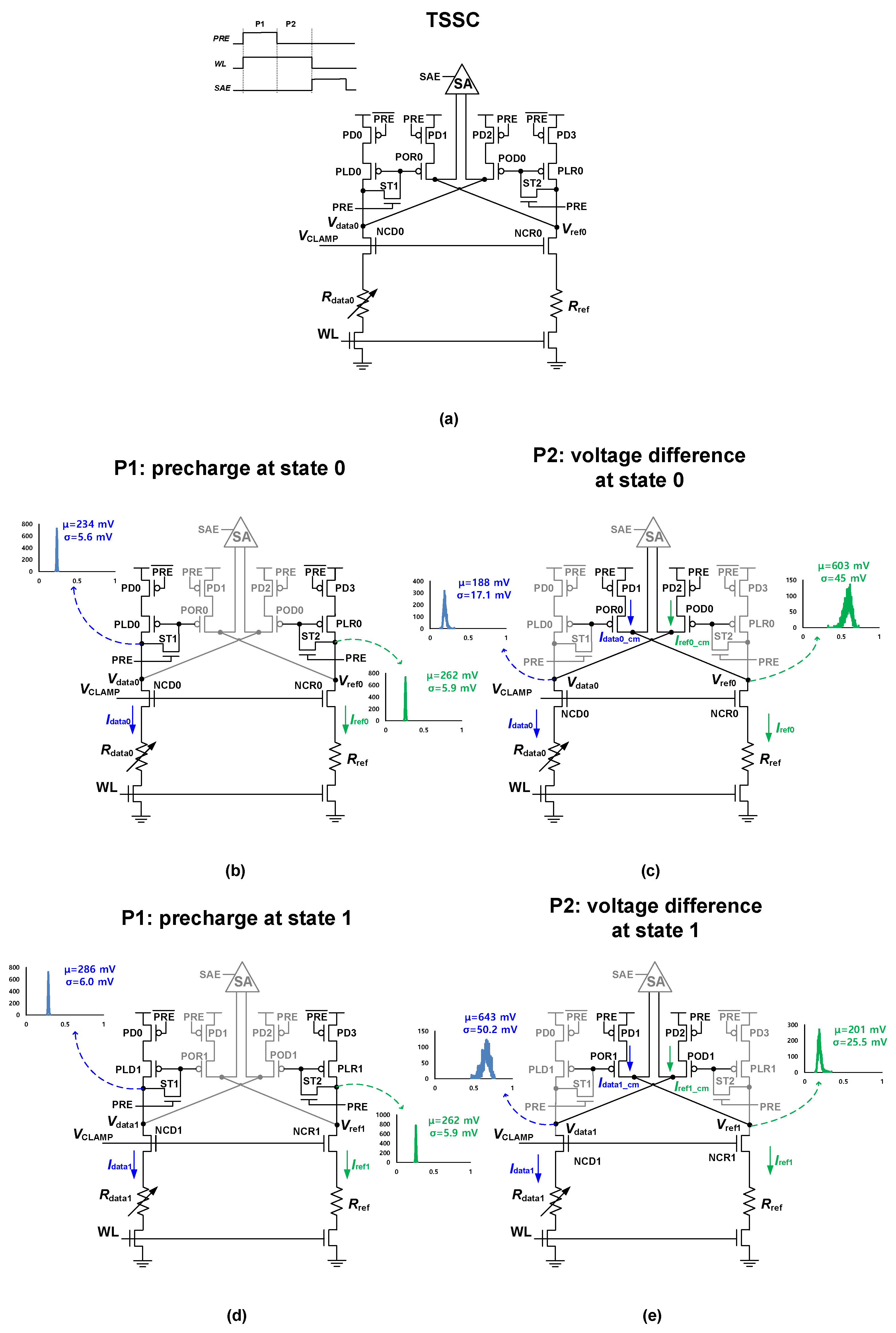
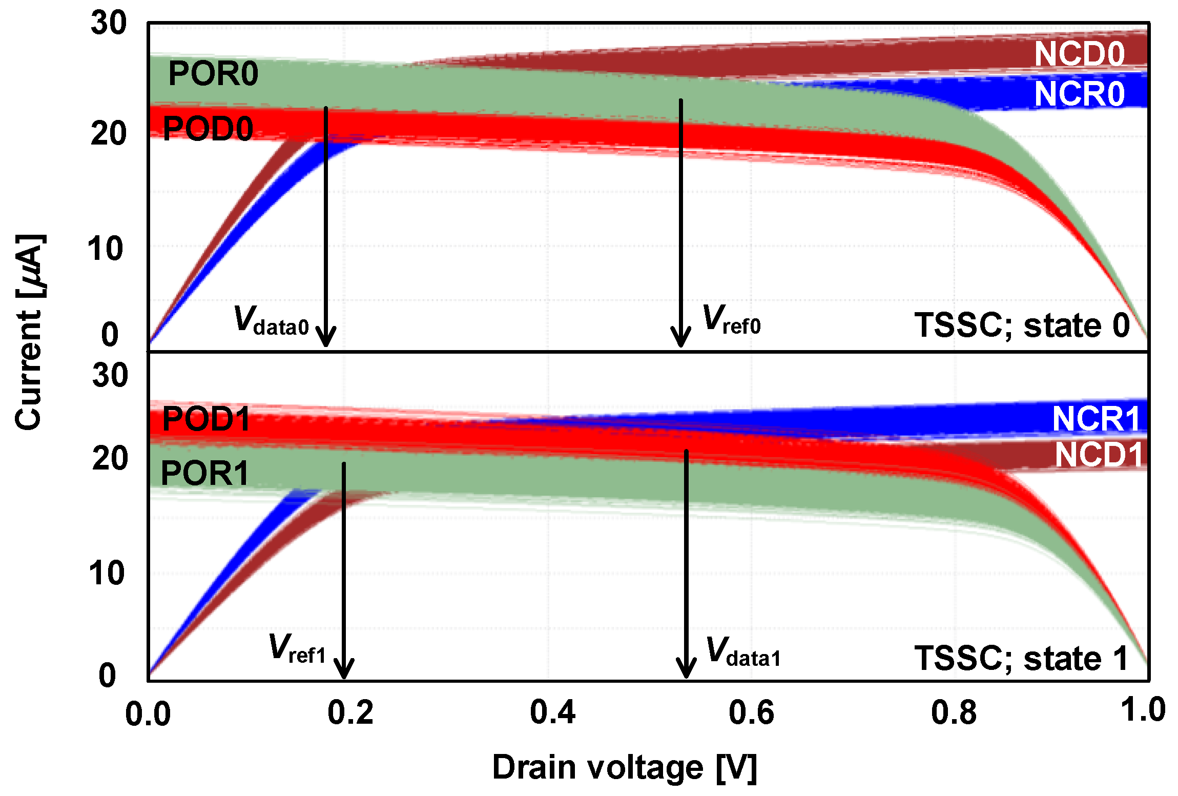
2.2. Proposed TSSC
3. Simulation Results
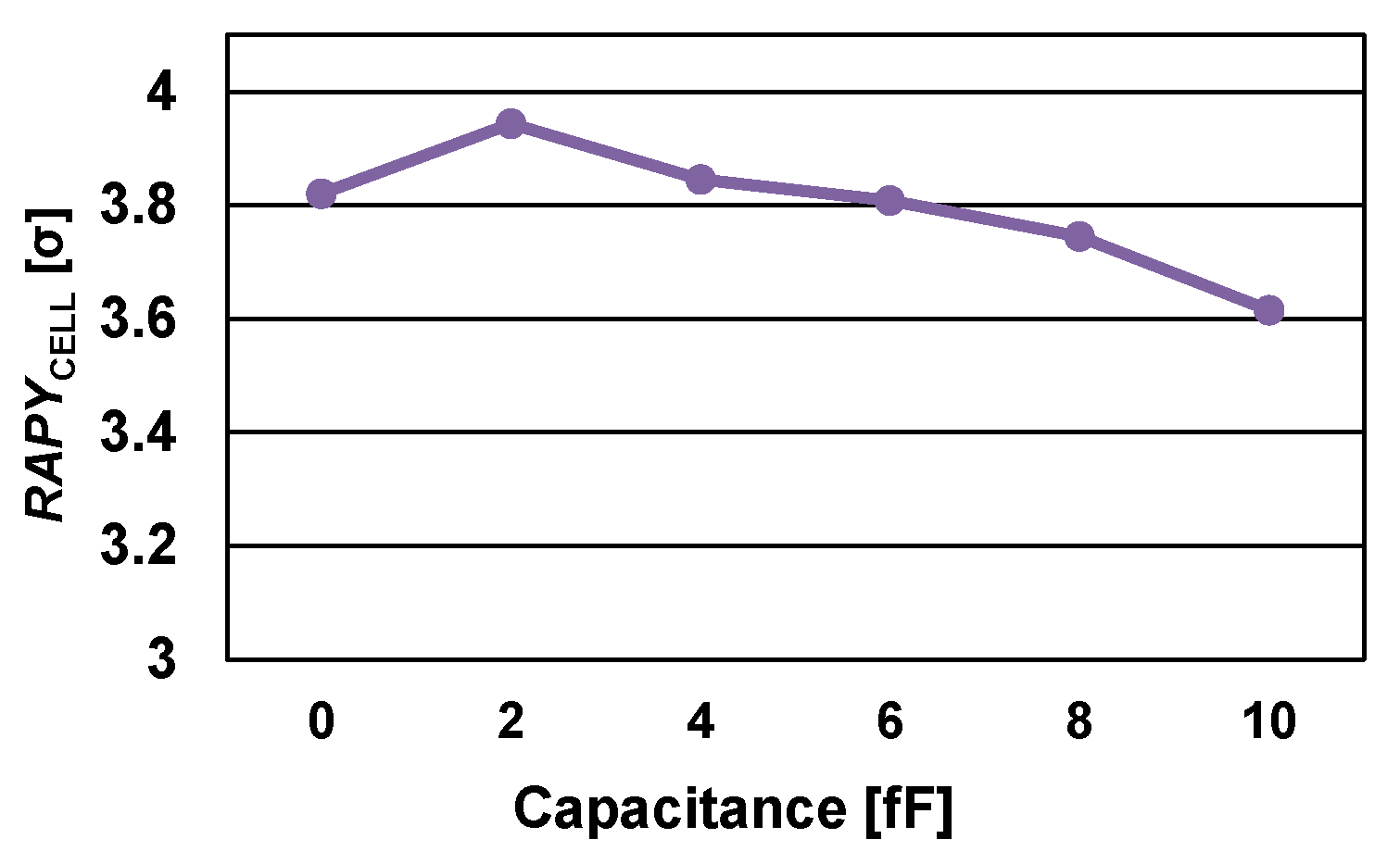
3.1. Simulation Conditions
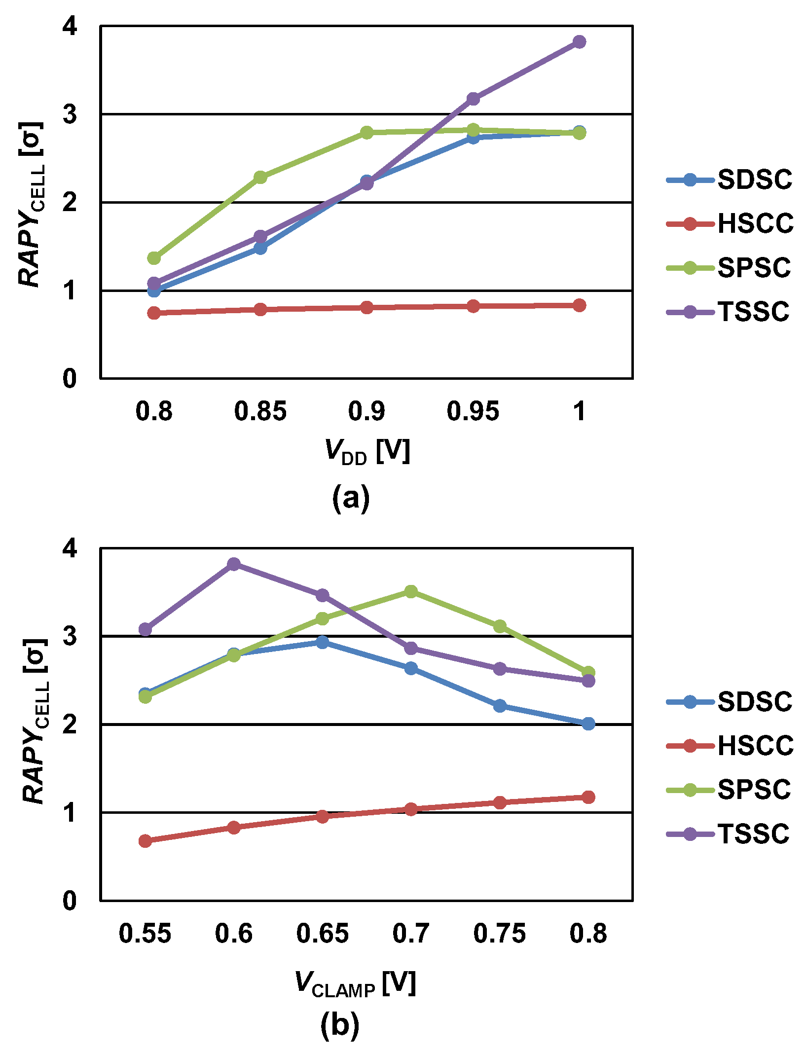
3.2. Results and Comparison
4. Conclusions
Author Contributions
Funding
Institutional Review Board Statement
Informed Consent Statement
Data Availability Statement
Acknowledgments
Conflicts of Interest
References
- Huang, W.; Liu, L.; Zhu, Z. A sub-200nW all-in-one bandgap voltage and current reference without amplifiers. IEEE Trans. Circuits Syst. II Exp. Briefs 2021, 1, 121–125. [Google Scholar] [CrossRef]
- Kim, C.; Kwon, K.; Park, C.; Jang, S.; Choi, J. A covalent-bonded cross-coupled current-mode sense amplifier for STT-MRAM with 1T1MTJ common source-line structure array. In Proceedings of the 2015 IEEE International Solid-State Circuits Conference—(ISSCC) Digest of Technical Papers, San Francisco, CA, USA, 22–26 February 2015; pp. 1–3. [Google Scholar]
- Hosomi, M.; Yamagishi, H.; Yamamoto, T.; Bessho, K.; Higo, Y.; Yamane, K.; Yamada, H.; Shoji, M.; Hachino, H.; Fukumoto, C.; et al. A novel nonvolatile memory with spin torque transfer magnetization switching: Spin-RAM. In Proceedings of the IEEE International Electron Devices Meeting, 2005. IEDM Technical Digest, Washington, DC, USA, 5 December 2005; pp. 459–462. [Google Scholar]
- Ikeda, S.; Miura, K.; Yamamoto, H.; Mizunuma, K.; Gan, H.D.; Endo, M.; Kanai, S.; Hayakawa, J.; Matsukura, F.; Ohno, H. A perpendicular-anisotropy CoFeB-MgO magnetic tunnel junction. Nat. Mater. 2010, 9, 721–724. [Google Scholar] [CrossRef] [PubMed]
- Takemura, R.; Kawahara, T.; Miura, K.; Yamamoto, H.; Hayakawa, J.; Matsuzaki, N.; Ono, K.; Yamanouchi, M.; Ito, K.; Takahashi, H.; et al. A 32-Mb SPRAM with 2T1R memory cell, localized bi-directional write driver and ‘1’/’0’ dual-array equalized reference scheme. IEEE J. Solid-State Circuits 2010, 4, 869–879. [Google Scholar] [CrossRef]
- Tsuchida, K.; Inaba, T.; Fujita, K.; Ueda, Y.; Shimizu, T.; Asao, Y.; Kajiyama, T.; Iwayama, M.; Sugiura, K.; Ikegawa, S.; et al. A 64Mb MRAM with Clamped-Reference and Adequate-Reference Schemes. In Proceedings of the 2010 IEEE International Solid-State Circuits Conference—(ISSCC), San Francisco, CA, USA, 7–11 February 2010; pp. 258–259. [Google Scholar]
- Driskill-Smith, A.; Apalkov, D.; Nikitin, V.; Tang, X.; Watts, S.; Lottis, D.; Moon, K.; Khvalkovskiy, A.; Kawakami, R.; Luo, X.; et al. Latest Advances and Roadmap for In-Plane and Perpendicular STT-RAM. In Proceedings of the 2011 3rd IEEE International Memory Workshop (IMW), Monterey, CA, USA, 22–25 May 2011; pp. 1–3. [Google Scholar]
- Tabrizi, F. Non-Volatile STT-RAM: A True Universal Memory; Grandis Inc.: Milpitas, CA, USA, 2009. [Google Scholar]
- Na, T.; Kim, J.; Kim, J.P.; Kang, S.H.; Jung, S.-O. Reference-scheme study and novel reference scheme for deep submicrometer STT-RAM. IEEE Trans. Circuits Syst. I Regul. Pap. 2014, 61, 3376–3385. [Google Scholar] [CrossRef]
- Kim, J.; Na, T.; Kim, J.P.; Kang, S.H.; Jung, S.-O. A split-path sensing circuit for spin torque transfer MRAM. IEEE Trans. Circuits Syst. II Exp. Briefs 2014, 3, 193–197. [Google Scholar] [CrossRef]
- Kim, J.; Ryu, K.; Kang, S.H.; Jung, S.-O. A novel sensing circuit for deep submicron spin transfer torque MRAM (STT-MRAM). IEEE Trans. Very Large Scale Integr. (VLSI) Syst. 2012, 1, 181–186. [Google Scholar] [CrossRef]
- Nho, H.; Yoon, S.; Wong, S.S.; Jung, S. Numerical Estimation of Yield in Sub-100-nm SRAM Design Using Monte Carlo Simulation. IEEE Trans. Circuits Syst. II Express Briefs 2008, 9, 907–911. [Google Scholar]
- Maffitt, T.M.; DeBrosse, J.K.; Gabric, J.A.; Gow, E.T.; Lamorey, M.C.; Parenteau, J.S.; Willmott, D.R.; Wood, M.A.; Gallagher, W.J. Design considerations for MRAM. IBM J. Res. Develop. 2012, 1, 181–186. [Google Scholar] [CrossRef]
- Trinh, Q.; Ruocco, S.; Alioto, M. Dynamic reference voltage sensing scheme for read margin improvement in STT-MRAMs. IEEE Trans. Circuits Syst. I 2018, 65, 1269–1278. [Google Scholar] [CrossRef]
- Datta, T.; Abshire, P. Mismatch compensation of CMOS current mirrors using floating-gate transistors. In Proceedings of the 2009 IEEE International Symposium on Circuits and Systems, Taipei, Taiwan, 24–27 May 2009. [Google Scholar]
- Lakshmikumar, K.R.; Hadaway, R.A.; Copeland, M.A. Characterisation and modeling of mismatch in MOS transistors for precision analog design. IEEE J. Solid-State Circuits 1986, 6, 1057–1066. [Google Scholar] [CrossRef] [Green Version]
- Na, T.; Woo, S.-H.; Kim, J.; Jeong, H.; Jung, S.-O. Comparative study of various latch-type sense amplifiers. IEEE Trans. Very Large Scale Integr. (VLSI) Syst. 2014, 2, 425–429. [Google Scholar] [CrossRef]


| SDSC [11] | HSSC [13] | SPSC [10] | TSSC (Proposed) | |
|---|---|---|---|---|
| Process technology | 28 nm | |||
| DRV technique | X | O | O | O |
| ICELL [μA] @ state 1 | 20.0 | |||
| Layout Area of SC [μm2] @ iso-area (Layout Area of SC [μm2] @ identical Tr. size(1)) | 1.76 (1.28) | 1.76 (3.04) | 1.76 (2.56) | 1.76 (1.76) |
| RAPYCELL(2) [σ] @ VDD = 1.0 V, iso-area (RAPYCELL(2) [σ] @ VDD = 1.0 V, identical Tr. size) | 3.3 (3.12) | 1.1 (1.19) | 3.3 (3.36) | 4.7 (4.7) |
| RAPYCELL(3) [σ] @ VDD = 1.0 V, iso-area (RAPYCELL(3) [σ] @ VDD = 1.0 V, identical Tr. size) | 2.80 (2.68) | 0.83 (0.89) | 2.78 (2.79) | 3.82 (3.82) |
| Average sensing time [ns] @ VDD = 1.0 V, iso-area (Average sensing time [ns] @ VDD = 1.0 V, identical Tr. size) | 7 (7) | 8 (8) | 8 (8) | 14 (14) |
| PAVG [μA] @ state 0, VDD = 1.0 V, iso-area (PAVG [μA] @ state 0, VDD = 1.0 V, identical Tr. size) | 50.1 (48.1) | 153 (213) | 53.0 (62.9) | 48.9 (48.9) |
| PAVG [μA] @ state 1, VDD = 1.0 V, iso-area (PAVG [μA] @ state 1, VDD = 1.0 V, identical Tr. size) | 46.6 (44.7) | 137 (188.7) | 47.0 (55.8) | 44.0 (44.0) |
Publisher’s Note: MDPI stays neutral with regard to jurisdictional claims in published maps and institutional affiliations. |
© 2022 by the authors. Licensee MDPI, Basel, Switzerland. This article is an open access article distributed under the terms and conditions of the Creative Commons Attribution (CC BY) license (https://creativecommons.org/licenses/by/4.0/).
Share and Cite
Ishdorj, B.; Kim, J.; Kim, J.H.; Na, T. A Timing-Based Split-Path Sensing Circuit for STT-MRAM. Micromachines 2022, 13, 1004. https://doi.org/10.3390/mi13071004
Ishdorj B, Kim J, Kim JH, Na T. A Timing-Based Split-Path Sensing Circuit for STT-MRAM. Micromachines. 2022; 13(7):1004. https://doi.org/10.3390/mi13071004
Chicago/Turabian StyleIshdorj, Bayartulga, Jeongyeon Kim, Jae Hwan Kim, and Taehui Na. 2022. "A Timing-Based Split-Path Sensing Circuit for STT-MRAM" Micromachines 13, no. 7: 1004. https://doi.org/10.3390/mi13071004
APA StyleIshdorj, B., Kim, J., Kim, J. H., & Na, T. (2022). A Timing-Based Split-Path Sensing Circuit for STT-MRAM. Micromachines, 13(7), 1004. https://doi.org/10.3390/mi13071004