
Wireless Photometry Prototype for Tri-Color Excitation and Multi-Region Recording

 , , , and
Abstract
:1. Introduction
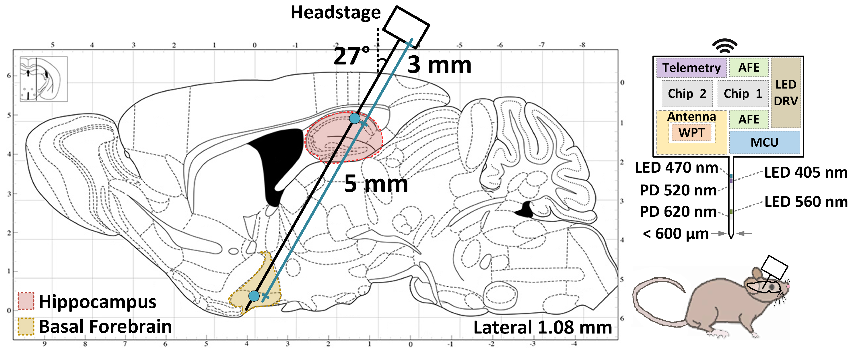
2. Target Application: Cholinergic Monitoring
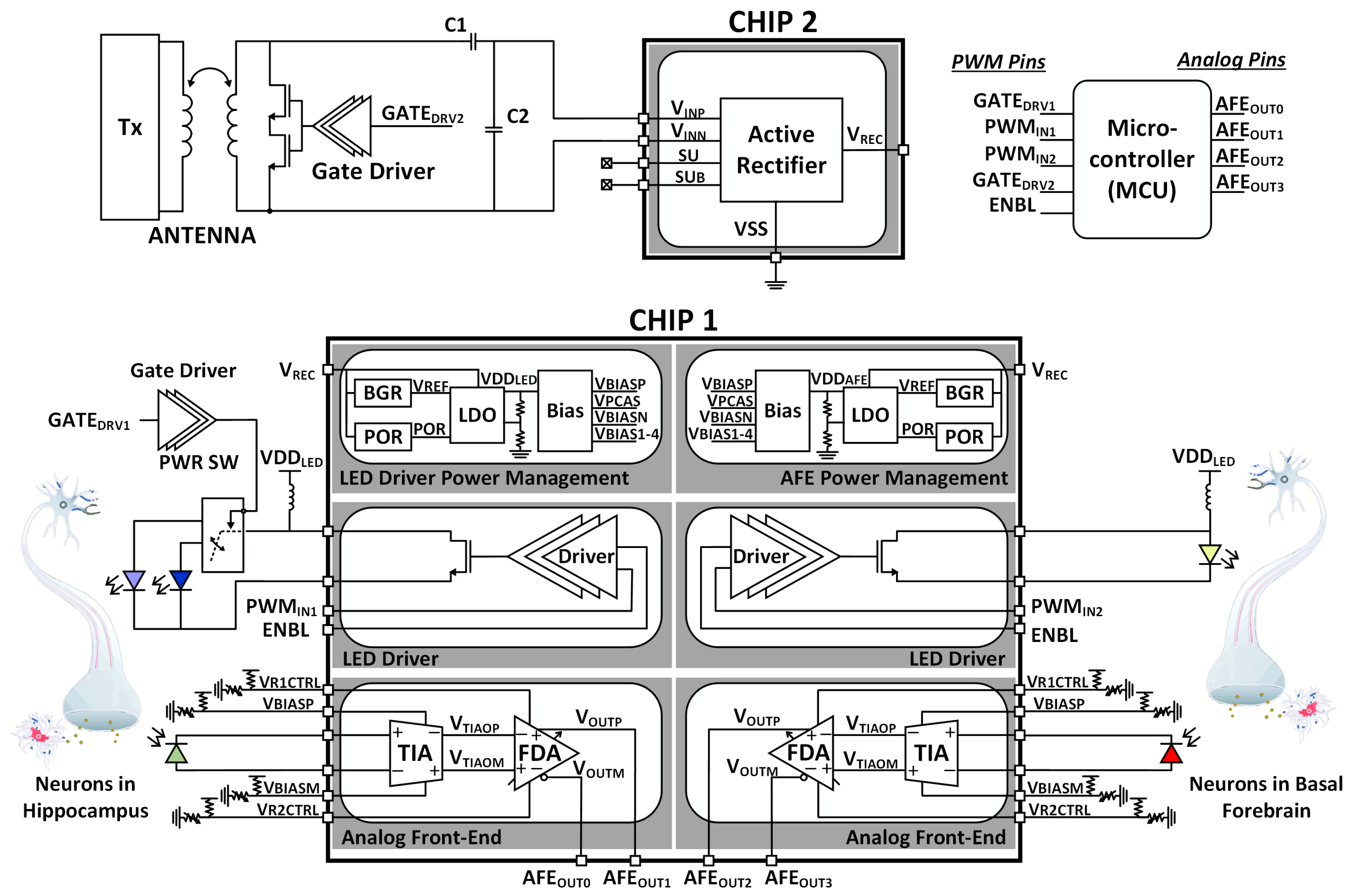
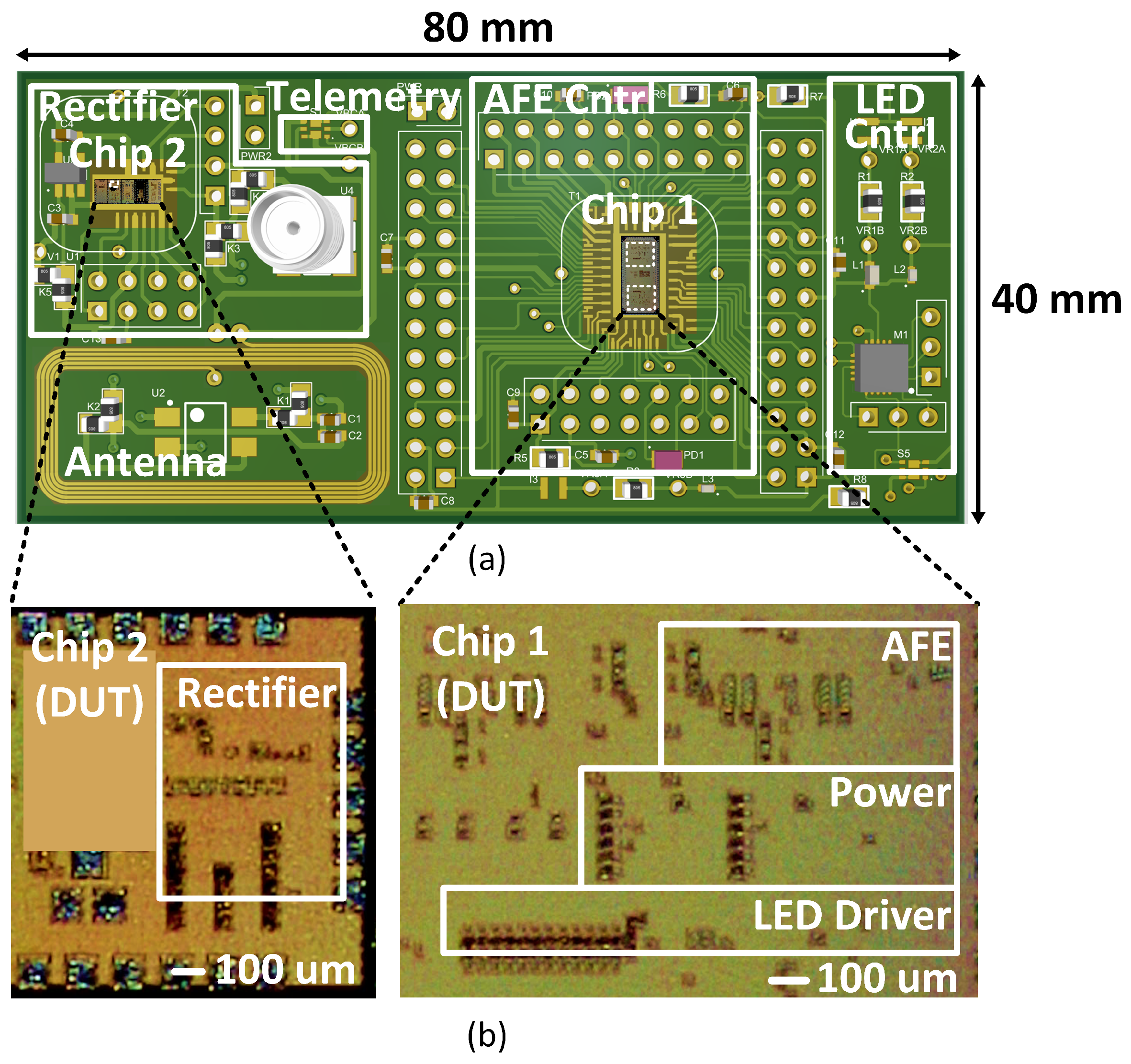
3. System Design
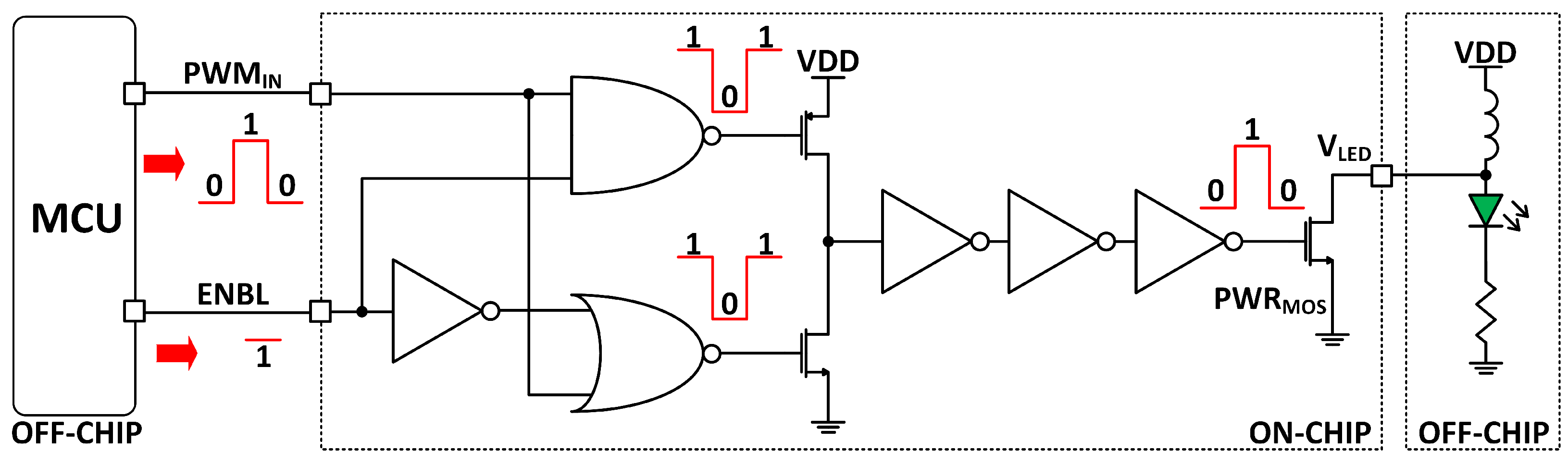
3.1. LED Driver
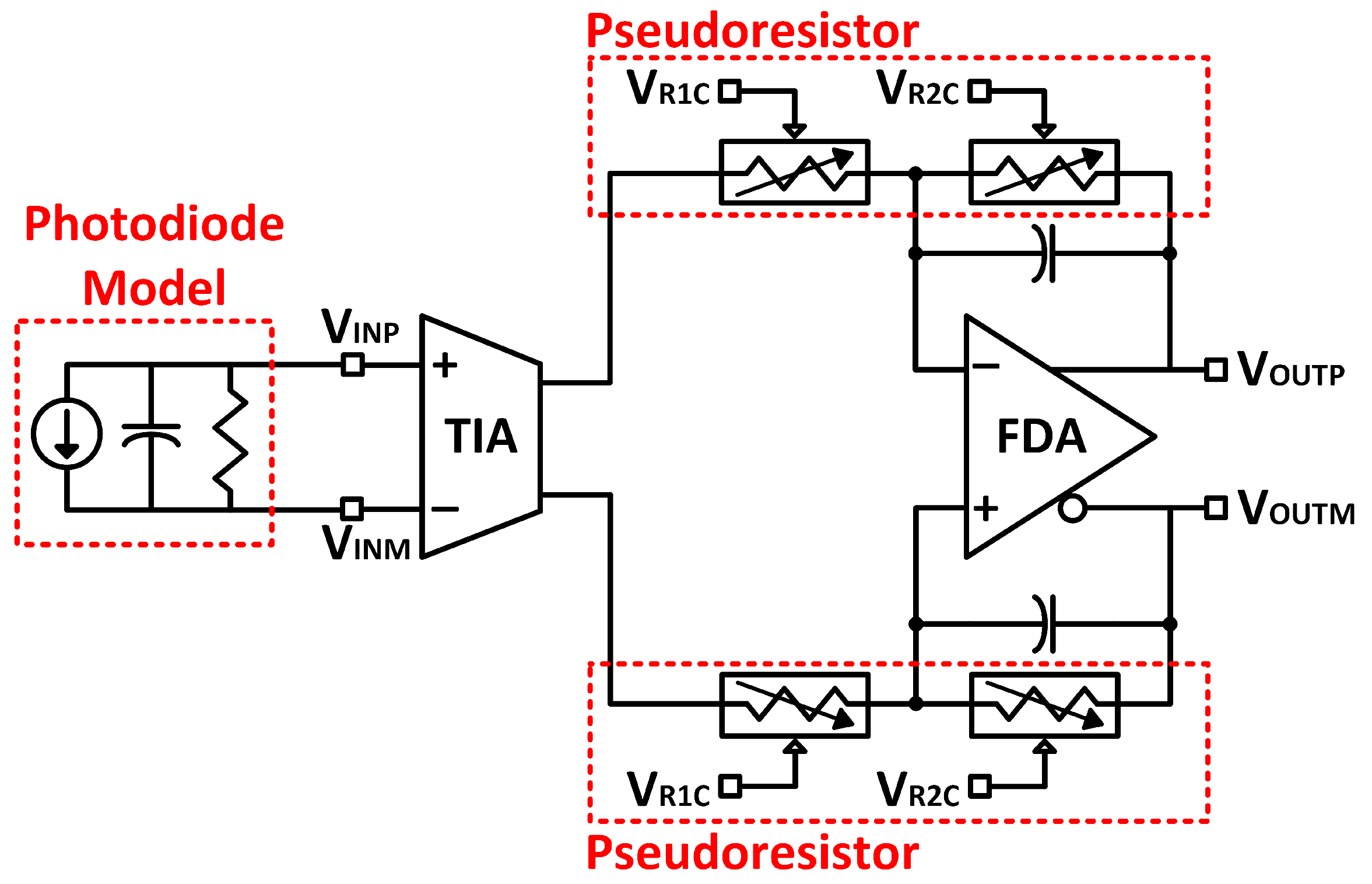
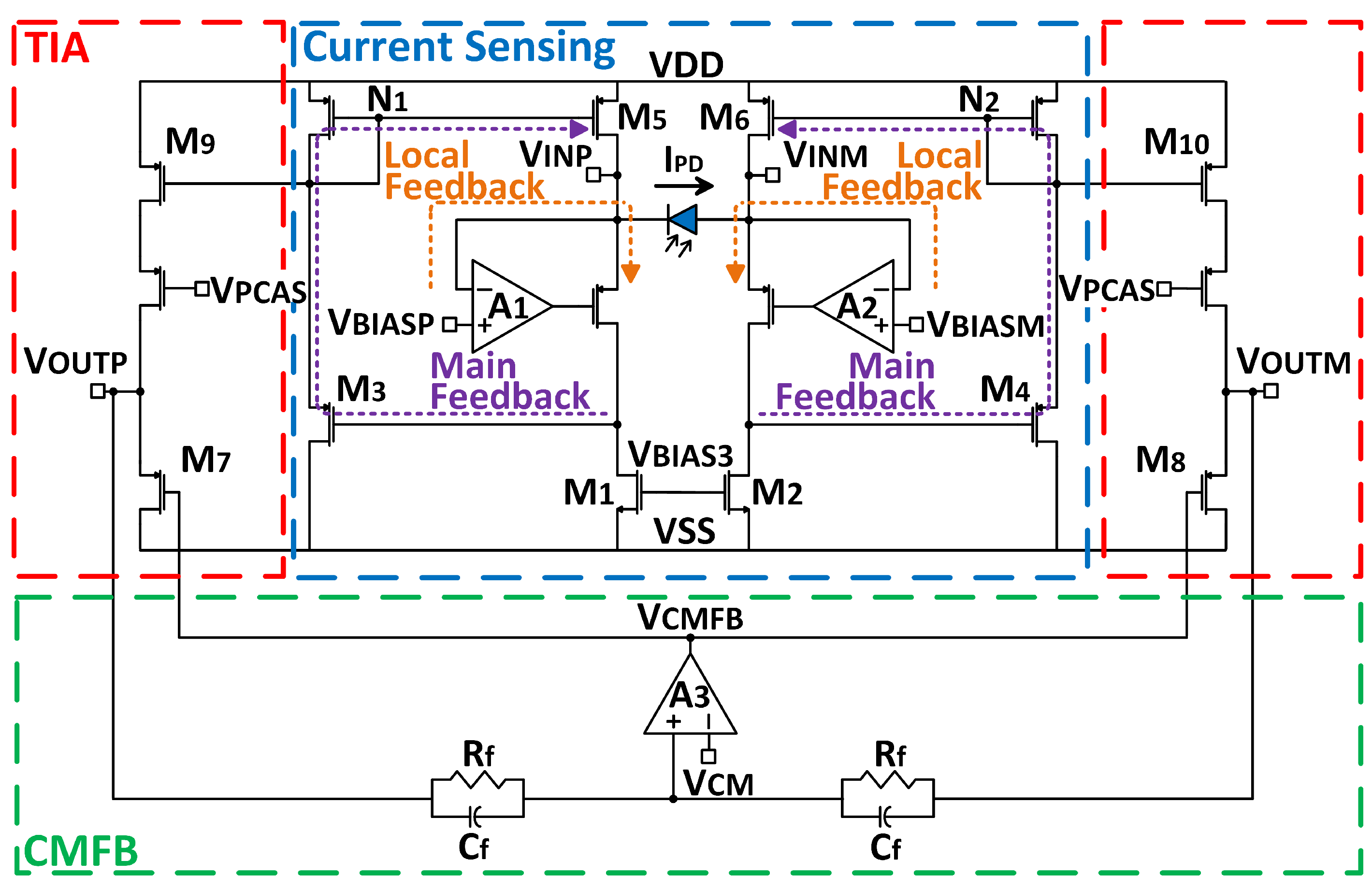
3.2. Analog Front-End (AFE)
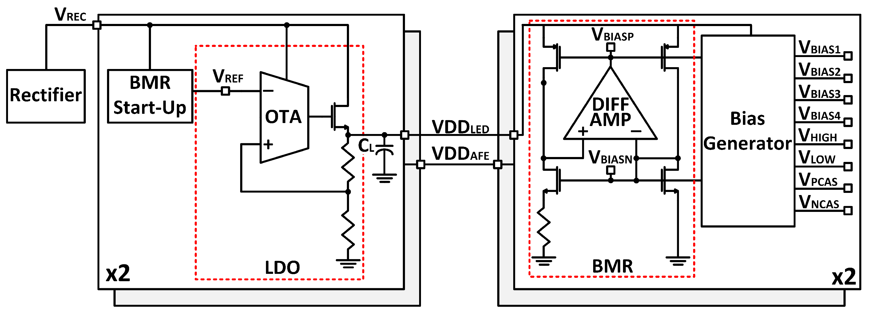
3.3. Power Management
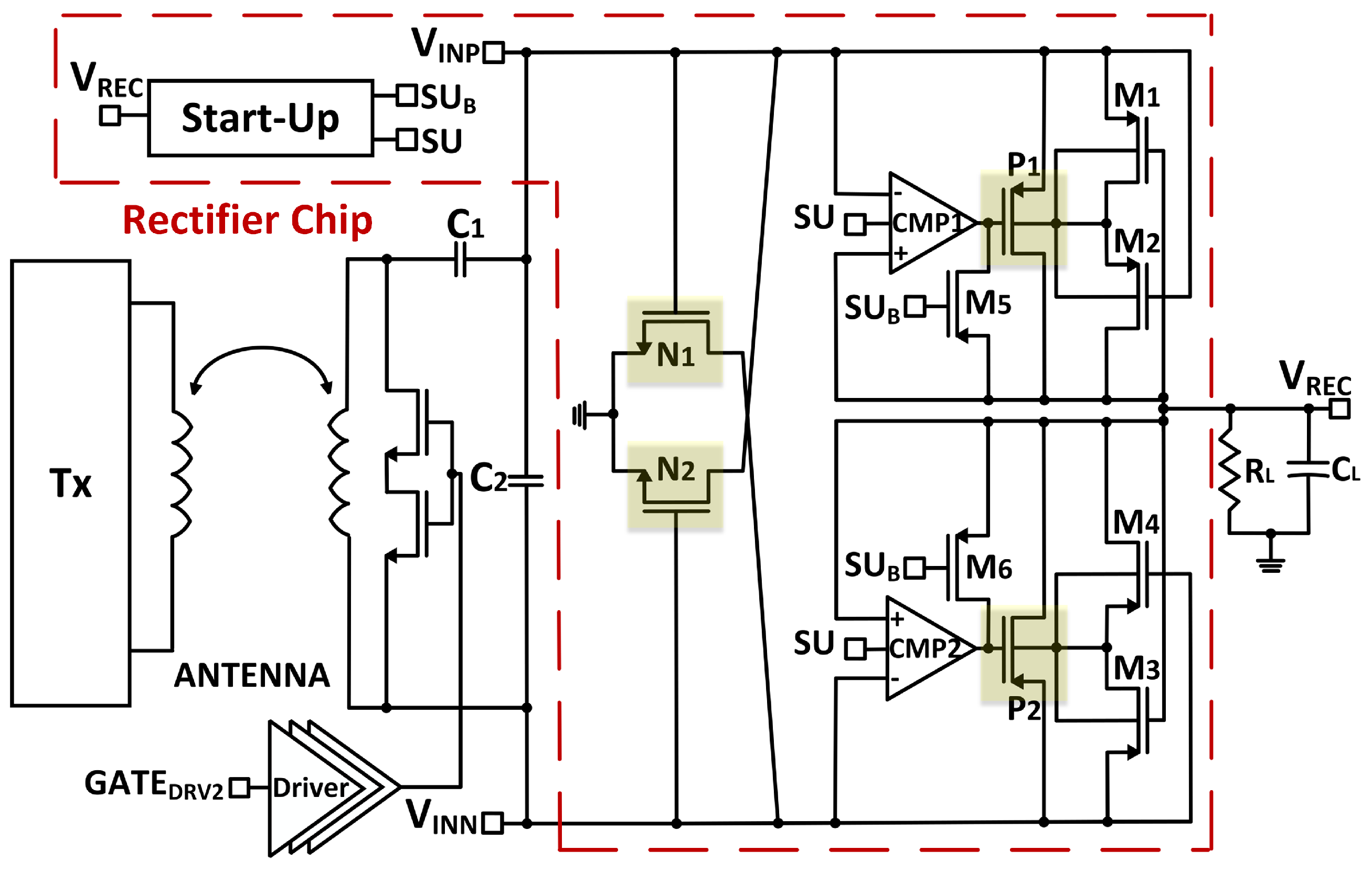
3.4. Wireless Power Transfer and Data Telemetry
4. Results and Discussion
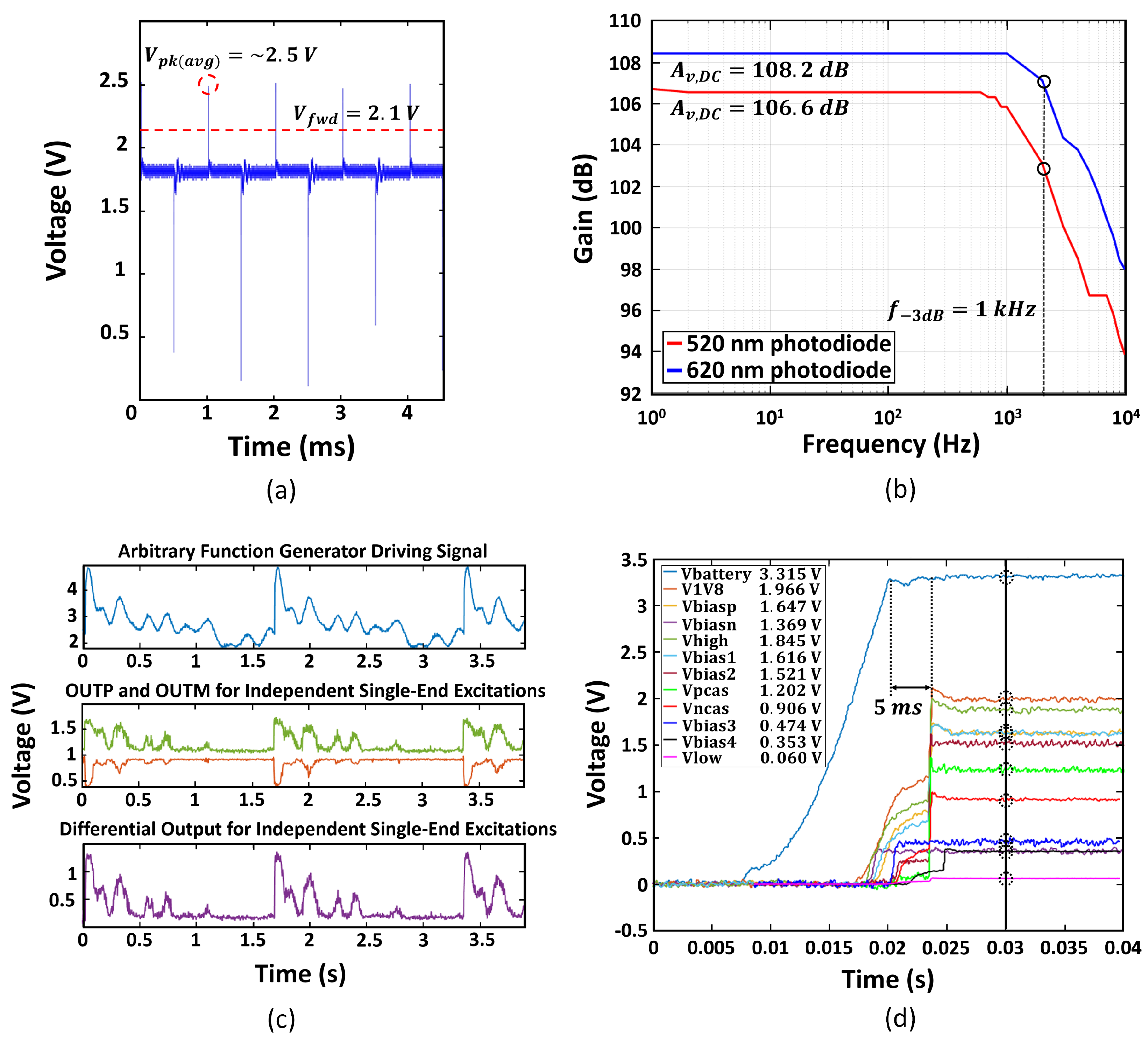
4.1. LED Driver Measurements
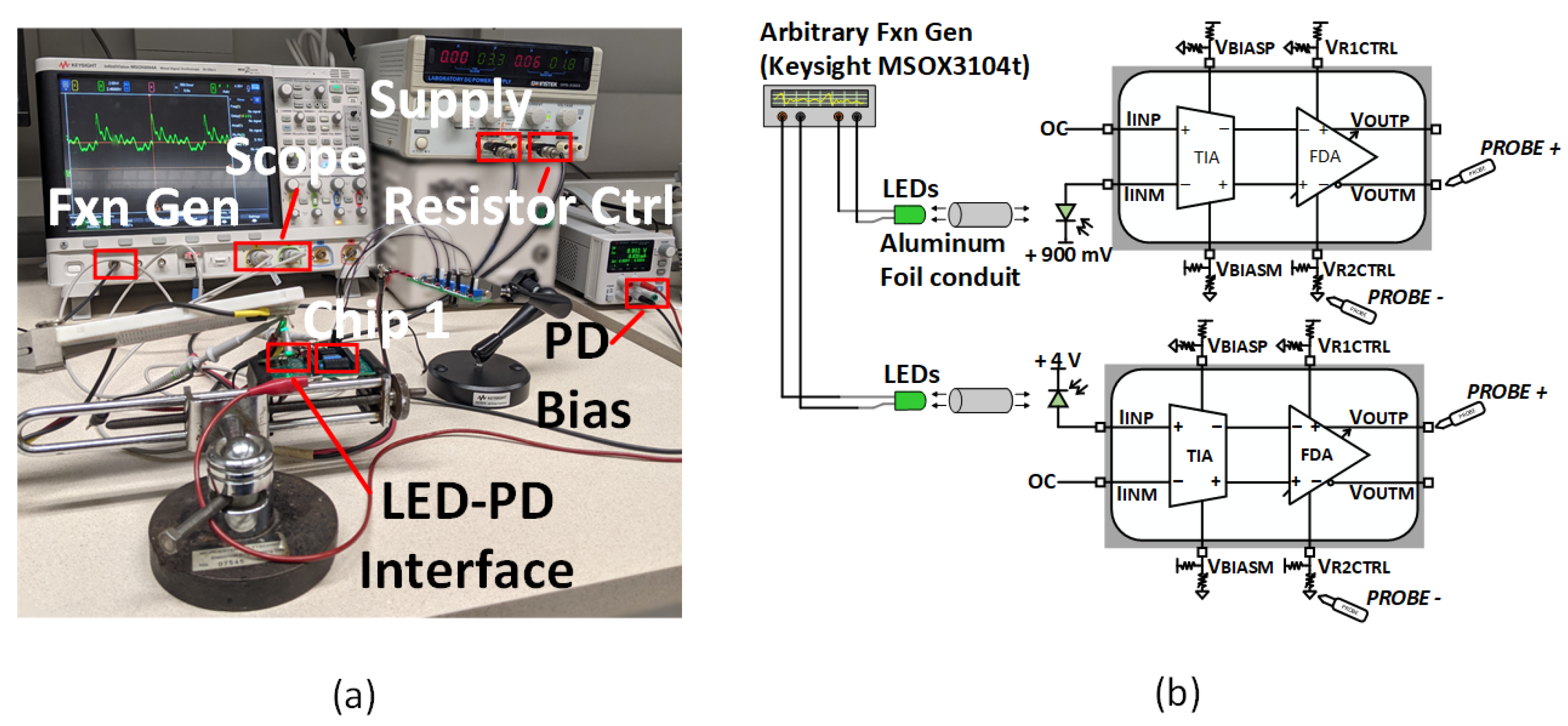
4.2. AFE Measurements
4.3. Power Management Measurements
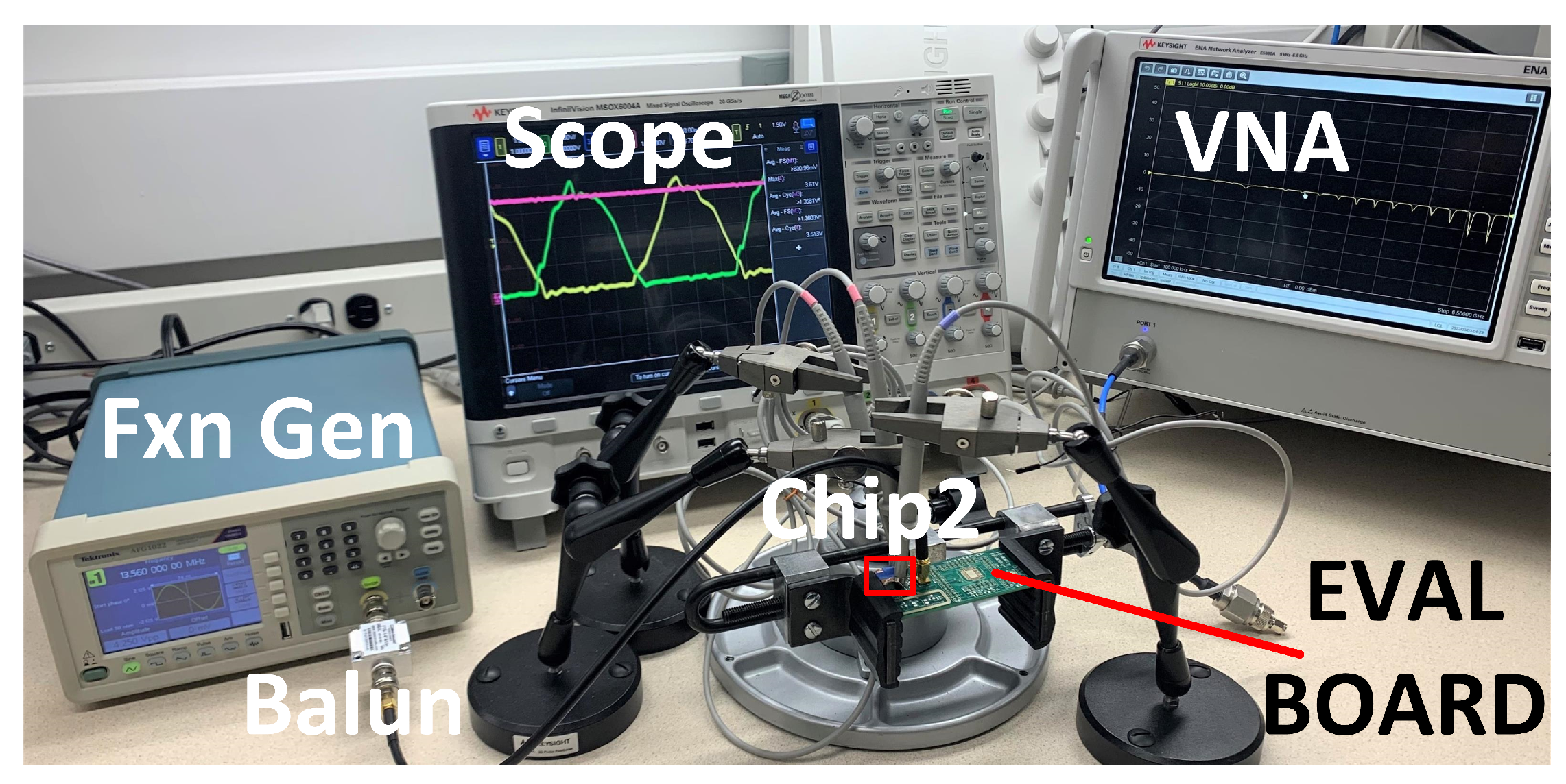
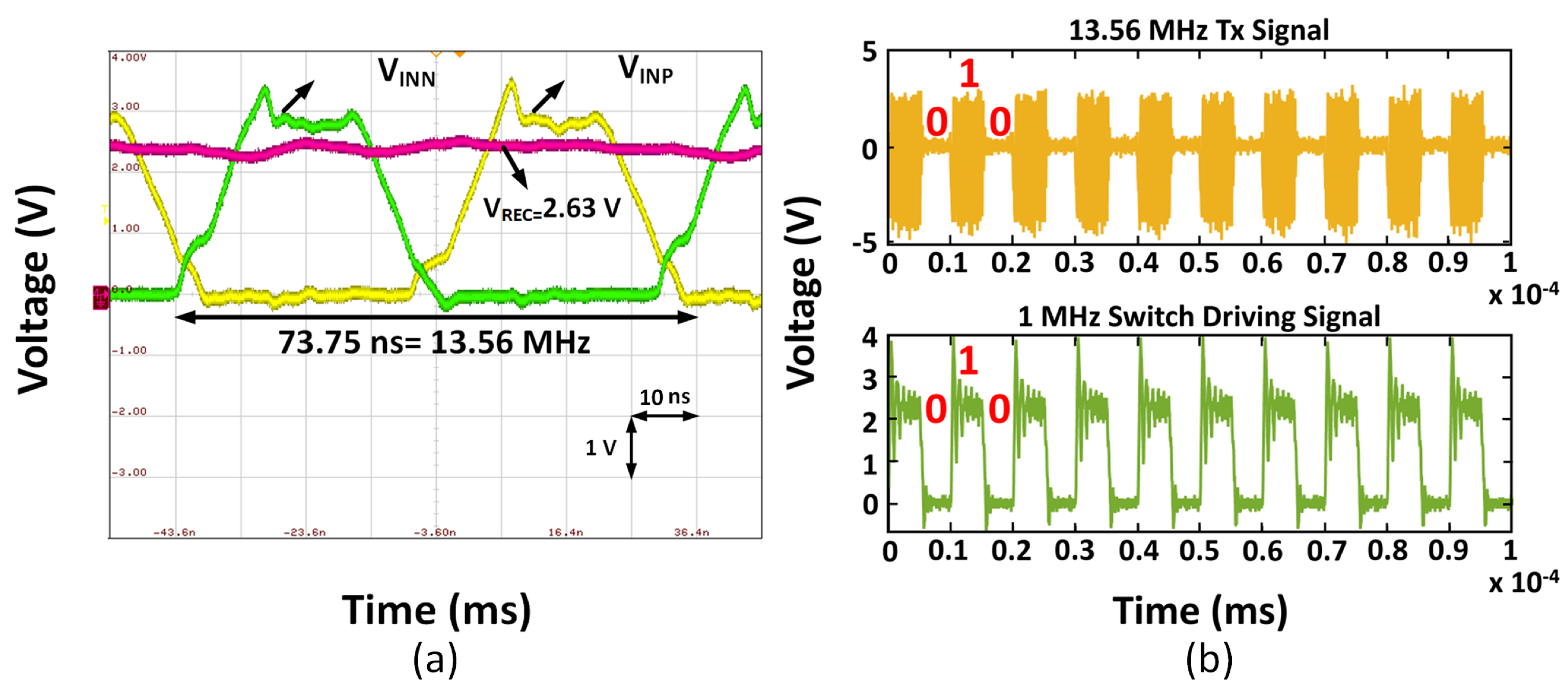
4.4. WPT and Data Telemetry Measurements
5. Benchmarking and Discussion
6. Conclusions
Author Contributions
Funding
Institutional Review Board Statement
Informed Consent Statement
Acknowledgments
Conflicts of Interest
References
- Dana, H.; Sun, Y.; Mohar, B.; Hulse, B.K.; Kerlin, A.M.; Hasseman, J.P.; Tsegaye, G.; Tsang, A.; Wong, A.; Patel, R.; et al. High-performance calcium sensors for imaging activity in neuronal populations and microcompartments. Nat. Methods 2019, 16, 649–657. [Google Scholar] [CrossRef]
- Dana, H.; Mohar, B.; Sun, Y.; Narayan, S.; Gordus, A.; Hasseman, J.P.; Tsegaye, G.; Holt, G.T.; Hu, A.; Walpita, D.; et al. Sensitive red protein calcium indicators for imaging neural activity. eLife 2019, 5, e12727. [Google Scholar] [CrossRef]
- Marvin, J.S.; Borghuis, B.G.; Tian, L.; Cichon, J.; Harnett, M.T.; Akerboom, J.; Gordus, A.; Renninger, S.L.; Chen, T.-W.; Bargmann, C.I.; et al. An optimized fluorescent probe for visualizing glutamate neurotransmission. Nat. Methods 2013, 10, 162–170. [Google Scholar] [CrossRef] [Green Version]
- Jing, M.; Li, Y.; Zeng, J.; Huang, P.; Skirzewski, M.; Kljakic, O.; Peng, W.; Qian, T.; Tan, K.; Zou, J.; et al. An optimized acetylcholine sensor for monitoring in vivo cholinergic activity. Nat. Methods 2020, 17, 1139–1146. [Google Scholar] [CrossRef] [PubMed]
- Sun, F.; Zeng, J.; Jing, M.; Zhou, J.; Feng, J.; Owen, S.F.; Luo, Y.; Li, F.; Wang, H.; Yamaguchi, T.; et al. A genetically-encoded fluorescent sensor enables rapid and specific detection of dopamine in flies, fish, and mice. Cell 2018, 174, 481–496.e19. [Google Scholar] [CrossRef] [PubMed]
- Patriarchi, T.; Cho, J.R.; Merten, K.; Howe, M.W.; Marley, A.; Xiong, W.-H.; Folk, R.W.; Broussard, G.J.; Liang, R.; Jang, M.J.; et al. Ultrafast neuronal imaging of dopamine dynamics with designed genetically encoded sensors. Science 2018, 360, eaat4422. [Google Scholar] [CrossRef] [Green Version]
- Inoue, M.; Takeuchi, A.; Manita, S.; Horigane, S.; Sakamoto, M.; Kawakami, R.; Yamaguchi, K.; Otomo, K.; Yokoyama, H.; Kim, R.; et al. Rational Engineering of XCaMPs, a Multicolor GECI Suite for In Vivo Imaging of Complex Brain Circuit Dynamics. Cell 2019, 177, 1346–1360. [Google Scholar] [CrossRef] [PubMed]
- Kim, C.K.; Yang, S.J.; Pichamoorthy, N.; Young, N.P.; Kauvar, I.; Jennings, J.H.; Lerner, T.N.; Berndt, A.; Lee, S.Y.; Ramakrishnan, C.; et al. Simultaneous fast measurement of circuit dynamics at multiple sites across the mammalian brain. Nat. Methods 2016, 13, 325–328. [Google Scholar] [CrossRef]
- Martianova, E.; Aronson, S.; Proulx, C.D. Multi-Fiber Photometry to Record Neural Activity in Freely-Moving Animals. J. Vis. Exp. 2019, 152, e60278. [Google Scholar] [CrossRef]
- Bartus, R.T.; Dean, R.L., 3rd; Beer, B.; Lippa, A.S. The Cholinergic Hypothesis of Geriatric Memory Dysfunction. Science 1982, 217, 408–414. [Google Scholar] [CrossRef] [PubMed]
- Chakravarti, A.; Tsuno, Y.; Guler, U. Towards a Tri-Color Wireless Photometry System for the Monitoring of Neuronal Activity in the Basal Forebrain and Hippocampus. In Proceedings of the 2021 43rd Annual International Conference of the IEEE Engineering in Medicine Biology Society (EMBC), Guadalajara, Mexico, 1–5 November 2021; pp. 7036–7039. [Google Scholar] [CrossRef]
- Paxinos, G.; Franklin, K.B.J. The Mouse Brain in Stereotaxic Coordinates, 2nd ed.; Academic Press: San Diego, CA, USA, 2001. [Google Scholar]
- Song, S.; Konijnenburg, M.; van Wegberg, R.; Xu, J.; Ha, H.; Sijbers, W.; Stanzione, S.; Biswas, D.; Breeschoten, A.; Vis, P.; et al. A 769 μW Battery-Powered Single-Chip SoC With BLE for Multi-Modal Vital Sign Monitoring Health Patches. IEEE Trans. Biomed. Circuits Syst. 2019, 13, 1506–1517. [Google Scholar] [CrossRef]
- Costanzo, I.; Sen, D.; Guler, U. An Integrated Readout Circuit for a Transcutaneous Oxygen Sensing Wearable Device. In Proceedings of the 2020 IEEE Custom Integrated Circuits Conference (CICC), Boston, MA, USA, 22–25 March 2020; pp. 1–4. [Google Scholar] [CrossRef]
- Lee, H.M.; Ghovanloo, M. An Integrated Power-Efficient Active Rectifier With Offset-Controlled High Speed Comparators for Inductively Powered Applications. IEEE Trans. Circuits Syst. I Regul. Pap. 2011, 58, 1749–1760. [Google Scholar] [CrossRef] [Green Version]
- Lee, H.M.; Ghovanloo, M. A High Frequency Active Voltage Doubler in Standard CMOS Using Offset-Controlled Comparators for Inductive Power Transmission. IEEE Trans. Biomed. Circuits Syst. 2013, 7, 213–224. [Google Scholar] [CrossRef] [PubMed] [Green Version]
- Ibrahim, T.S.; Abraham, D.; Rennaker, R.L. Electromagnetic Power Absorption and Temperature Changes due to Brain Machine Interface Operation. Ann. Biomed. Eng. 2007, 35, 825–834. [Google Scholar] [CrossRef]
- Guler, U.; Jia, Y.; Ghovanloo, M. A Reconfigurable Passive RF-to-DC Converter for Wireless IoT Applications. IEEE Trans. Circuits Syst. II Express Br. 2019, 66, 1800–1804. [Google Scholar] [CrossRef]
- Kampasi, K.; English, D.F.; Seymour, J.; Stark, E.; McKenzie, S.; Vöröslakos, M.; Buzsáki, G.; Wise, K.D.; Yoon, E. Dual color optogenetic control of neural populations using low-noise, multishank optoelectrodes. Microsyst. Nanoeng. 2018, 4, 10. [Google Scholar] [CrossRef] [PubMed] [Green Version]
- Brunert, D.; Tsuno, Y.; Rothermel, M.; Shipley, M.T.; Wachowiak, M. Cell-Type-Specific Modulation of Sensory Responses in Olfactory Bulb Circuits by Serotonergic Projections from the Raphe Nuclei. J. Neurosci. 2016, 36, 6820–6835. [Google Scholar] [CrossRef] [PubMed]
- Jia, Y.; Gong, Y.; Weber, A.; Li, W.; Ghovanloo, M. A mm-Sized Free-Floating Wireless Implantable Opto-Electro Stimulation Device. Micromachines 2020, 11, 621. [Google Scholar] [CrossRef] [PubMed]
- Yousefi, T.; Taghadosi, M.; Dabbaghian, A.; Siu, R.; Grau, G.; Zoidl, G.; Kassiri, H. An Energy-Efficient Optically-Enhanced Highly-Linear Implantable Wirelessly-Powered Bidirectional Optogenetic Neuro-Stimulator. IEEE Trans. Biomed. Circuits Syst. 2020, 14, 1274–1286. [Google Scholar] [CrossRef] [PubMed]
- Jia, Y.; Guler, U.; Lai, Y.P.; Gong, Y.; Weber, A.; Li, W.; Ghovanloo, M. A Trimodal Wireless Implantable Neural Interface System-on-Chip. IEEE Trans. Biomed. Circuits Syst. 2020, 14, 1207–1217. [Google Scholar] [CrossRef] [PubMed]


| Parameters | MDPI ’20 [21] | TBIOCAS ’20 [22] | TBIOCAS ’20 [23] | Nature ’18 [19] | MDPI ’22 [This Work] |
|---|---|---|---|---|---|
| Technology | 0.35u | 0.13u | 0.35u | NM | 0.18u |
| Recording (AFE) | |||||
| Modality | NA | Electrical | Electrical | Electrical | Optical |
| Gain (dB) | NA | 48 | 55–70 | NA | 106–108 |
| Bandwidth (Hz) | NA | 1k | 1–100, 10k | 20k | 1.1k |
| Power (uW) | NA | 160 | 800 | 320 | 620 |
| No. of channels | NA | 2 | 16 | 32 | 2 |
| Excitation/Stimulation | |||||
| Modality | Optical | Optical | Optical | Optical | Optical |
| Supply Voltage (V) | 5 | 3.3 | 4 | NM | 1.8 |
| Peak current (mA) | 12 | 15 | 24.8 | NM | 20 |
| Optical Power (uW) | NM | 85.3 | NM | NM | 1–300 |
| No. of colors | 1 | 1 | 1 | 2 | 3 |
| No. of channels | 16 | 2 | 16 | 32 | 3 |
| LED (nm) | 470 | 488 568 | 460 | 405 635 | 405 470 560 |
| WPT and Telemetry | |||||
| Structure | 3-coil | 2-coil | 4-coil | NA | 2-coil |
| Meas. PCE (%) | 43 | NM | 82 | NA | 63 |
| Load ()/() | NM/10 | NM/200 | NM/NM | NA | 500/10 |
| WPT Freq (MHz) | 60 | 85.86 | 13.56 | NA | 13.56 |
| Optimum (V) | 4.2 | 3.3 | 4.2 | NA | 2.63 |
| Data Modulation | OOK | NM | OOK-PPM | NA | OOK |
Publisher’s Note: MDPI stays neutral with regard to jurisdictional claims in published maps and institutional affiliations. |
© 2022 by the authors. Licensee MDPI, Basel, Switzerland. This article is an open access article distributed under the terms and conditions of the Creative Commons Attribution (CC BY) license (https://creativecommons.org/licenses/by/4.0/).
Share and Cite
Chakravarti, A.; Marangalou, A.H.; Costanzo, I.M.; Sen, D.; Sciulli, M.; Tsuno, Y.; Guler, U. Wireless Photometry Prototype for Tri-Color Excitation and Multi-Region Recording. Micromachines 2022, 13, 727. https://doi.org/10.3390/mi13050727
Chakravarti A, Marangalou AH, Costanzo IM, Sen D, Sciulli M, Tsuno Y, Guler U. Wireless Photometry Prototype for Tri-Color Excitation and Multi-Region Recording. Micromachines. 2022; 13(5):727. https://doi.org/10.3390/mi13050727
Chicago/Turabian StyleChakravarti, Aatreya, Amin Hazrati Marangalou, Ian Matthew Costanzo, Devdip Sen, Mirco Sciulli, Yusuke Tsuno, and Ulkuhan Guler. 2022. "Wireless Photometry Prototype for Tri-Color Excitation and Multi-Region Recording" Micromachines 13, no. 5: 727. https://doi.org/10.3390/mi13050727
APA StyleChakravarti, A., Marangalou, A. H., Costanzo, I. M., Sen, D., Sciulli, M., Tsuno, Y., & Guler, U. (2022). Wireless Photometry Prototype for Tri-Color Excitation and Multi-Region Recording. Micromachines, 13(5), 727. https://doi.org/10.3390/mi13050727