
Static High Voltage Actuation of Piezoelectric AlN and AlScN Based Scanning Micromirrors


 ,
,  , ,
, ,
Abstract
:1. Introduction
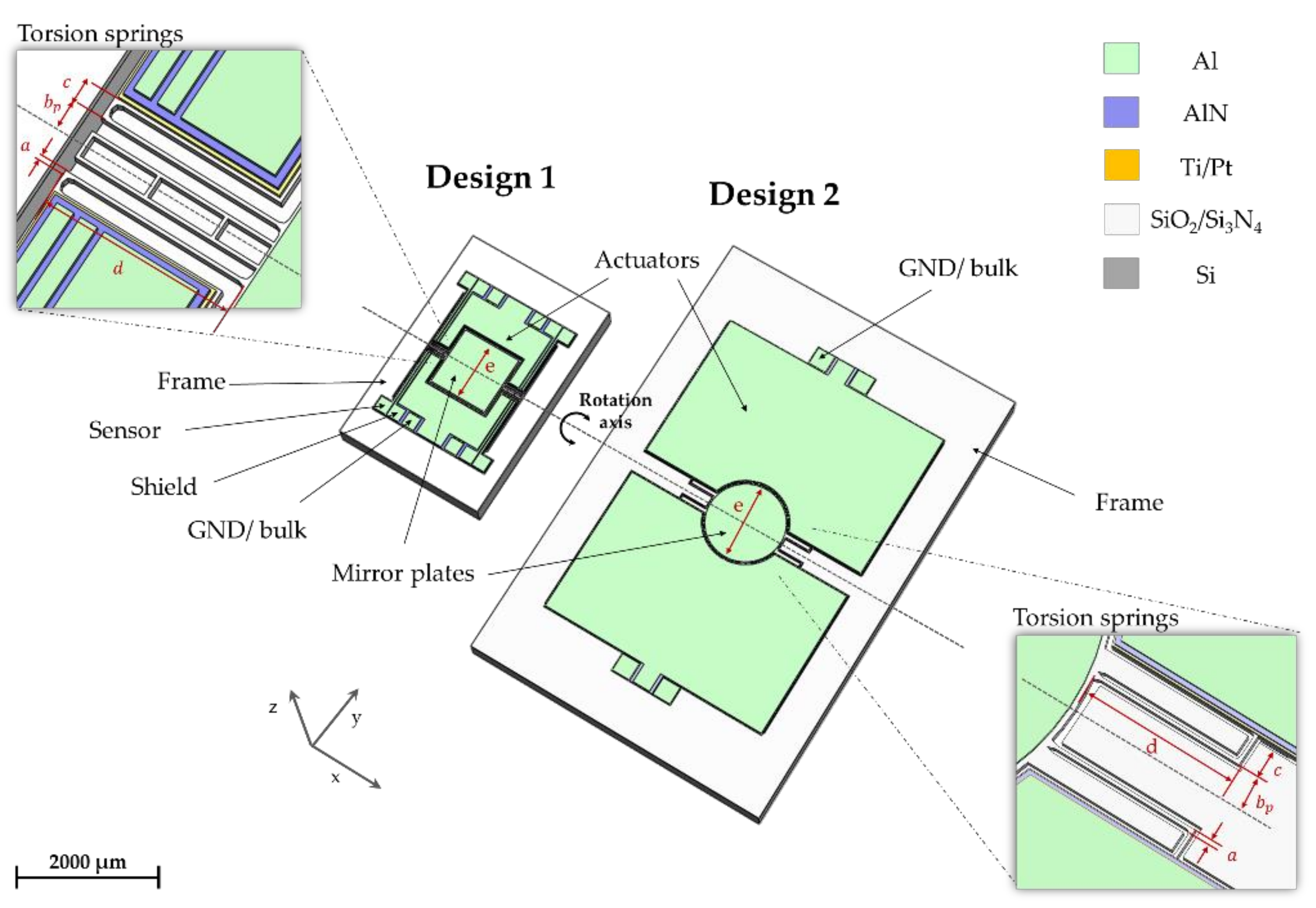
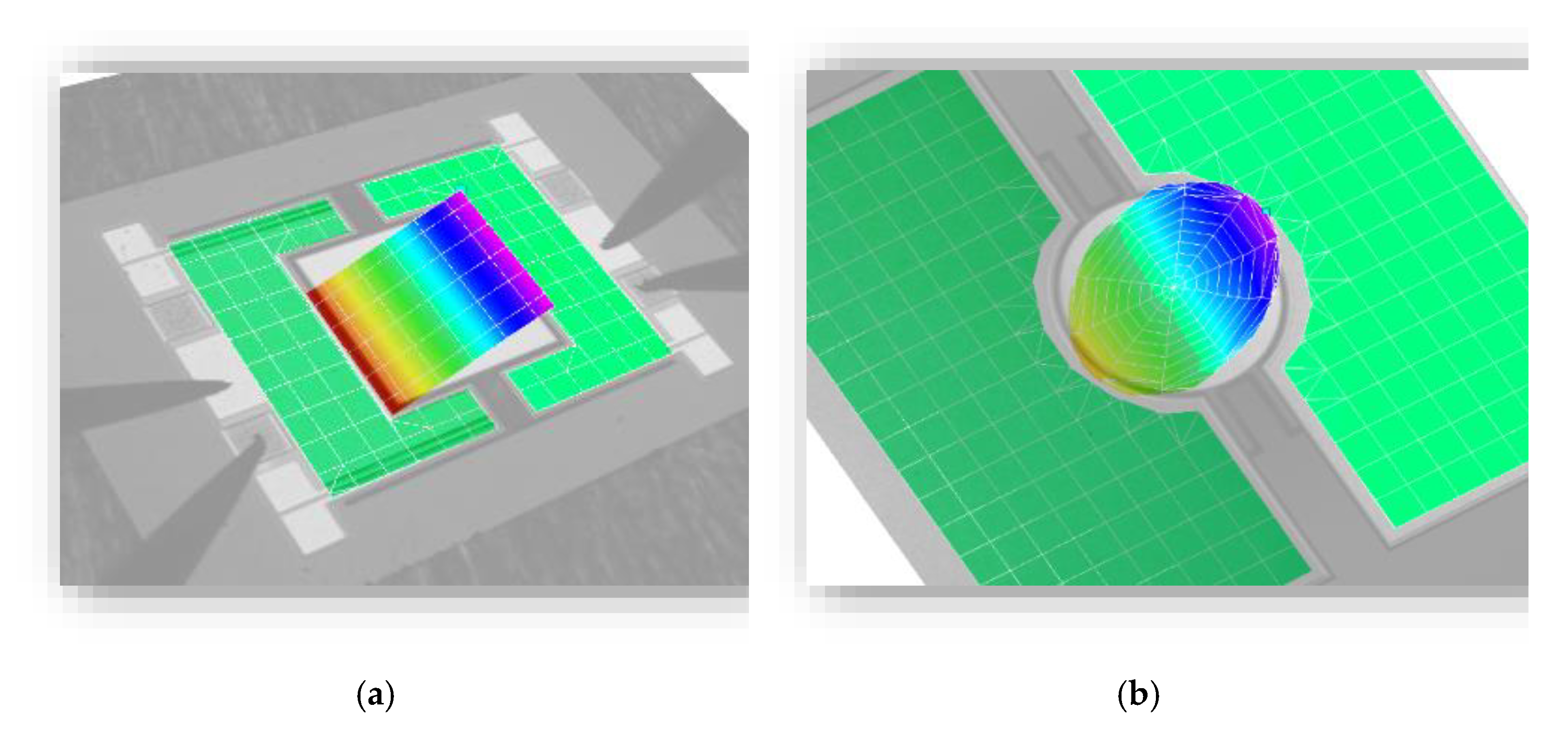
2. Design
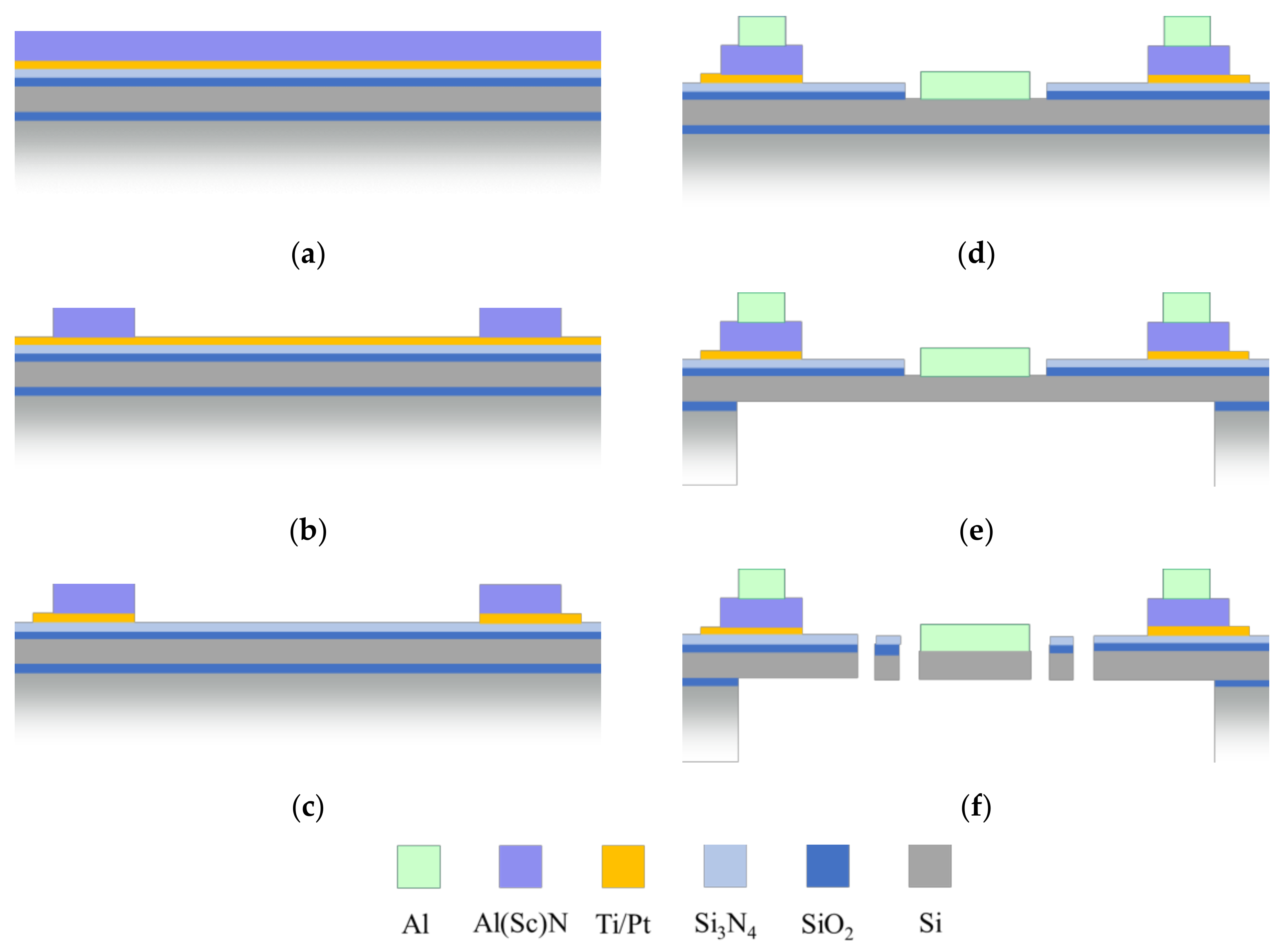
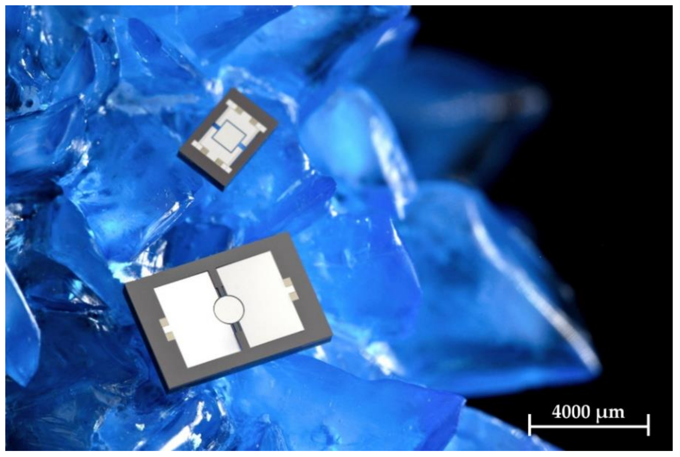
3. Fabrication
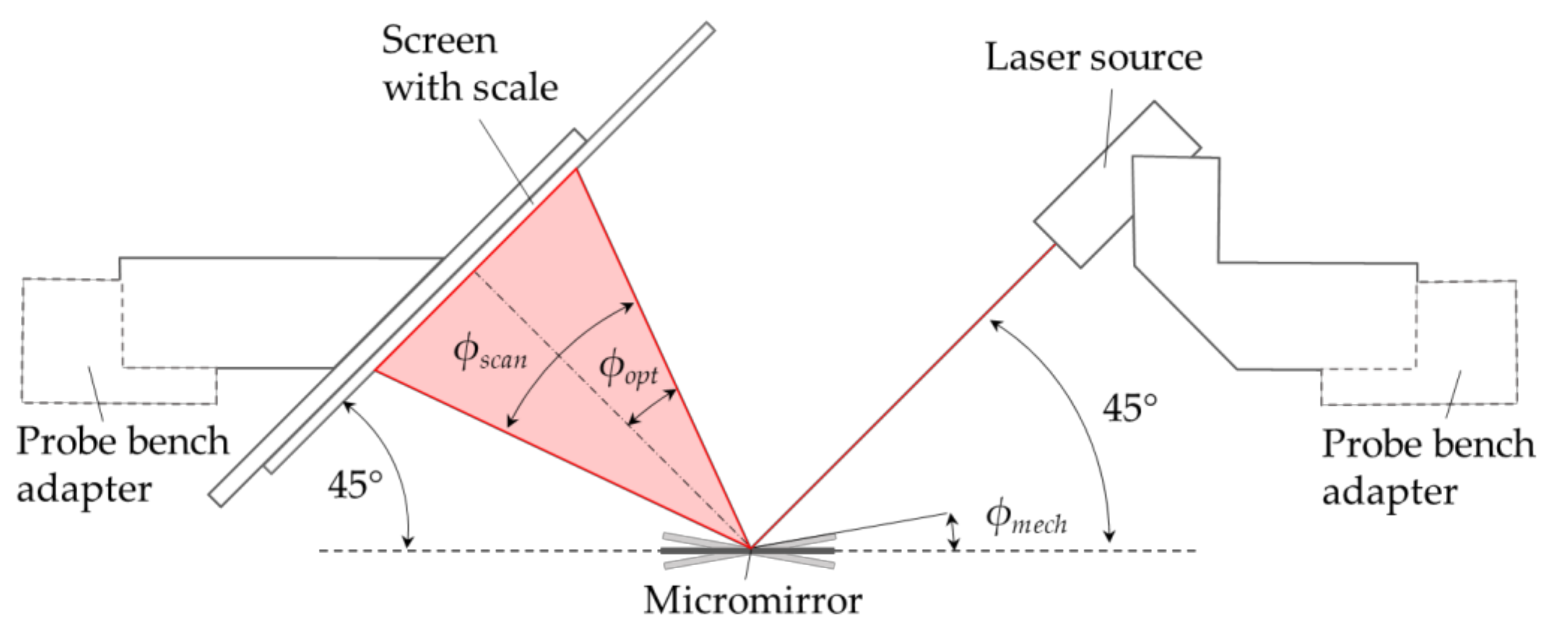
4. Measurement Setup
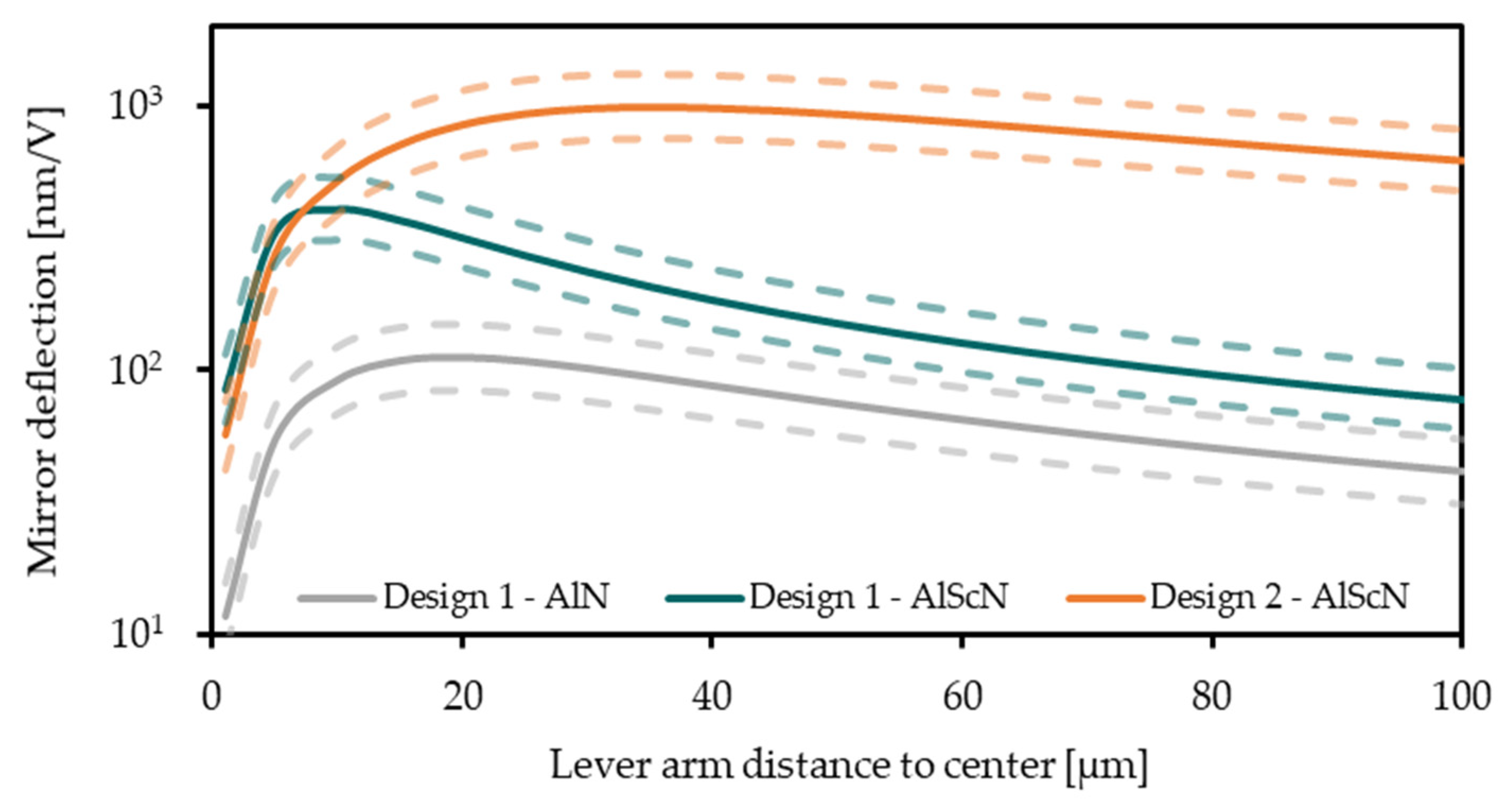
5. Results and Discussion
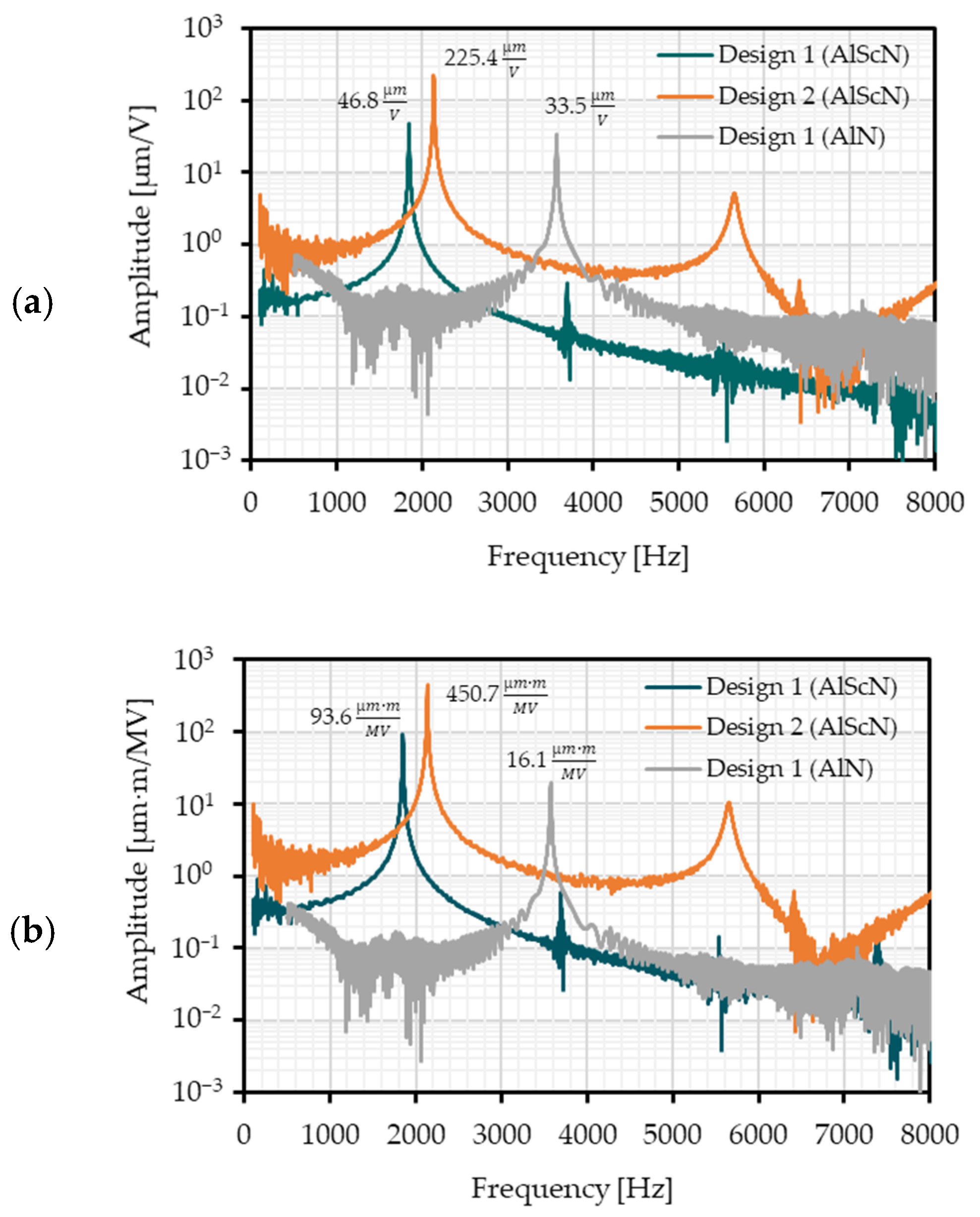
5.1. Frequency Response and Small Signal Actuation
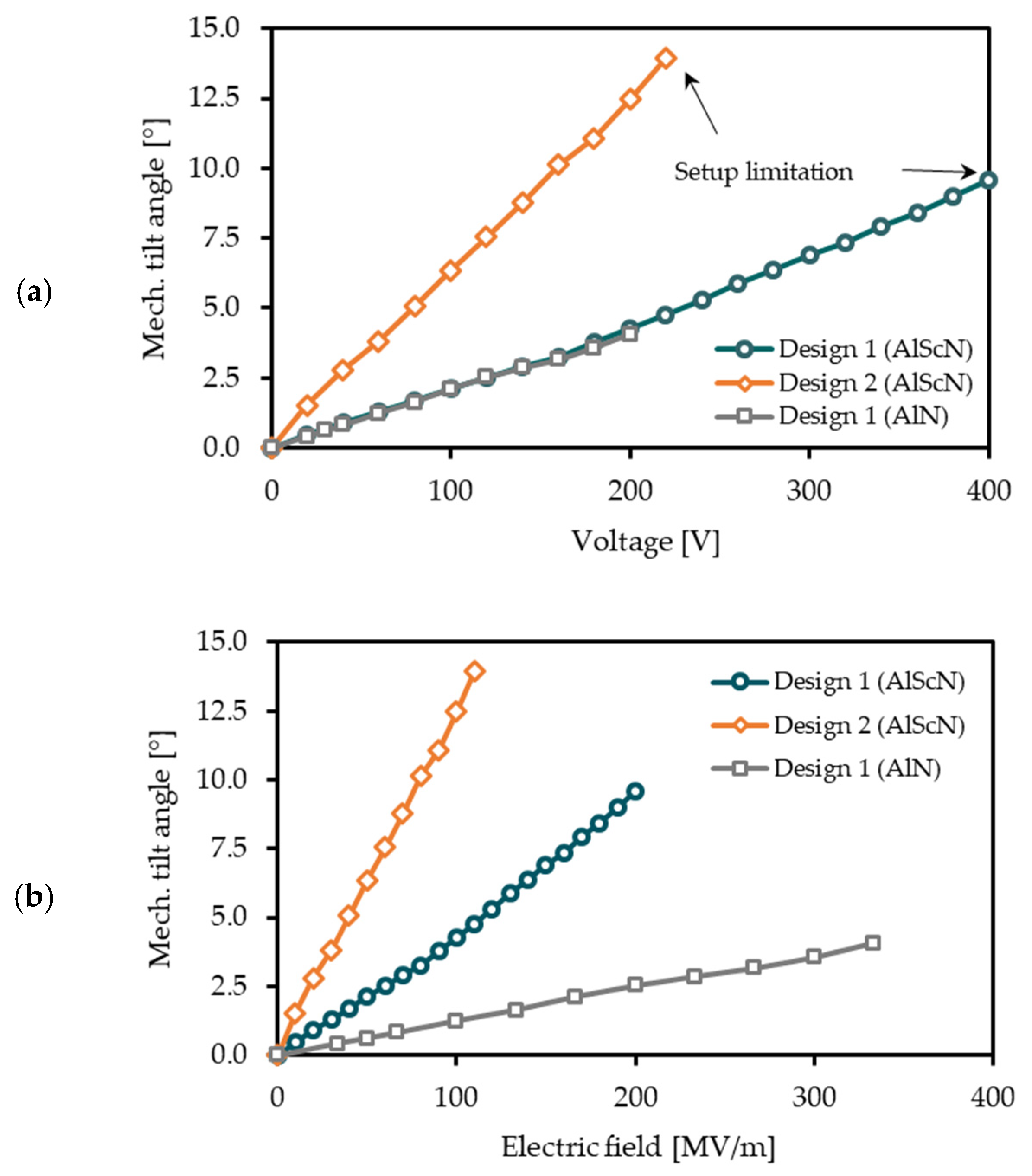
5.2. Static High Voltage Actuation
6. Conclusions
Author Contributions
Funding
Conflicts of Interest
References
- Holmström, S.T.S.; Baran, U. MEMS Laser Scanners: A Review. J. Microelectromech. Syst. 2014, 23, 259–275. [Google Scholar] [CrossRef]
- Patterson, P.R.; Hah, D. Scanning micromirrors: An overview. Proc. SPIE 2004, 5604, 195–207. [Google Scholar] [CrossRef]
- Xie, H. Editorial for the Special Issue on MEMS Mirrors. Micromachines 2018, 9, 99. [Google Scholar] [CrossRef] [PubMed] [Green Version]
- Specht, H. MEMS-Laser-Display-System: Analyse, Implementierung und Testverfahrenentwicklung. Ph.D. Thesis, Chemnitz Universitiy of Technology, Chemnitz, Germany, 2011. [Google Scholar]
- Schenk, H. Ein Neuartiger Mikroaktor zur Ein-Und Zweidimensionalen Ablenkung von Licht. Ph.D. Thesis, Gerhard-Mercator-Universität-Gesamthochschule-Duisburg, Duisburg, Germany, 2000. [Google Scholar]
- Shao, J.; Li, Q. AlN based piezoelectric micromirror. Opt. Lett. 2018, 43, 987–990. [Google Scholar] [CrossRef] [PubMed]
- Meinel, K.; Stoeckel, C.; Melzer, M. Piezoelectric scanning micromirror with large scan angle based on thin film aluminum nitride. In Proceedings of the 20th International Conference on Solid-State Sensors, Actuators and Microsystems and Eurosensors XXXIII (Transducers & Eurosensors XXXIII), Berlin, Germany, 23–27 June 2019. [Google Scholar]
- Meinel, K.; Stoeckel, C. Piezoelectric scanning micromirror with built-in sensors based on thin film aluminum nitride. IEEE Sens. J. 2020, 21, 9682–9689. [Google Scholar] [CrossRef]
- Meinel, K.; Melzer, M. 2D Scanning Micromirror with Large Scan Angle and Monolithically Integrated Angle. Sensors 2020, 20, 6599. [Google Scholar] [CrossRef] [PubMed]
- Senger, F.; Gu-Stoppel, S. A 2D circular-scanning piezoelectric MEMS mirror for laser material processing. Proc. SPIE 2021, 11697, 1169704. [Google Scholar] [CrossRef]
- Pensala, T.; Kyynäräinen, J. Wobbling mode AlN-piezo-mems mirror enabling 360-degree field of view LIDAR for automotive applications. In Proceedings of 2019 IEEE International Ultrasonics Symposium (IUS), Glasgow, Scotland, 6–9 October 2019. [Google Scholar]
- Senger, F.; Albers, J. A bi-axial vacuum-packaged piezoelectric MEMS mirror for smart headlights. Proc. SPIE 2020, 11293, 1129305. [Google Scholar] [CrossRef]
- Kobayashi, T.; Maeda, R. Piezoelectric Optical Micro Scanner with Built-in Torsion Sensors. Jpn. J. Appl. Phys. 2007, 46, 2781–2784. [Google Scholar] [CrossRef]
- Gu-Stoppel, S.; Lisec, T. A highly linear piezoelectric quasi-static MEMS mirror with mechanical tilt angles of larger than 10°. Proc. SPIE 2019, 10931, 1093102. [Google Scholar] [CrossRef]
- Lu, Y.; Reusch, M. Surface Morphology and Microstructure of Pulsed DC Magnetron Sputtered Piezoelectric AlN and AlScN Thin Films. Phys. Status Solidi A 2018, 215, 1700559. [Google Scholar] [CrossRef]
- Lu, Y.; Reusch, M. Elastic modulus and coefficient of thermal expansion of piezoelectric Al1−xScxN (up to x = 0.41) thin films. APL Mater. 2018, 6, 076105. [Google Scholar] [CrossRef] [Green Version]


| Symbol 1 | Design 1 AlN | Design 1 AlScN | Design 2 AlScN | |
|---|---|---|---|---|
| General parameter | ||||
| Piezoelectric layer | AlN | Al0.68Sc0.32N | Al0.68Sc0.32N | |
| Thickness of piezoelectric layer [nm] | 600 | 2000 | 2000 | |
| Electric field at 1 V [MV/m] | 1.67 | 0.5 | 0.5 | |
| Silicon side wall shift [µm] | ~0.85 | ~1.35 | ~1.35 | |
| PVD parameter | ||||
| Nitrogen concentration [%] | 100 | 100 | 100 | |
| Pressure [Pa] | 0.7 | 0.36 | 0.36 | |
| Substrate temperature [°C] | 350 | 300 | 300 | |
| DC power [W] | 2120 | 625 (Al) + 375 (Sc) | 625 (Al) + 375 (Sc) | |
| Geometrical parameter | ||||
| Spring width (mask) [µm] | 5 | 5 | 7 | |
| Spring width (fabricated) [µm] | ′ | ~3.3 | ~2.3 | ~4.3 |
| Lever arm distance to center [µm] | 40 | 40 | 80 | |
| Distance to center of area [µm] | 200 | 200 | 187.5 | |
| Lever arm distance to actuator [µm] | 20 | 20 | 70 | |
| Spring length [µm] | 255 | 255 | 1030 | |
| Mirror plate length/diameter [µm] | 800 | 800 | 1000 | |
| Actuator width (quarter model) [µm] | 140 440 | 140 440 | 1000 505 | |
| Actuator length (quarter model) [µm] | 760 360 | 760 360 | 2020 1710 | |
| Parameter for analytical calculation | ||||
| Number of actuators in the model | 4 | 4 | 4 | |
| Thickness silicon substrate [µm] | 21 ± 10% | 21 ± 10% | 21 ± 10% | |
| PE charge coefficient [pm/V] | −2 ± 10% | −5 ± 10% | −5 ± 10% | |
| Resonance frequency [kHz] | 3.5 ± 10% | 2 ± 10% | 2 ± 10% | |
| E-Modulus of PE transducer [GPa] | 108 | 108 | 108 | |
| E-Modulus of silicon [GPa] | 63.9 | 63.9 | 63.9 | |
| Actuation voltage [V] | 1.0 | 1.0 | 1.0 | |
| Mass of the mirror plate [ng] | m | 31 ± 10% | 31 ± 10% | 38 ± 10% |
| Parameters 1 | Design 1 | Design 1 | Design 2 | |
|---|---|---|---|---|
| 600 nm AlN | 2000 nm Al0.68Sc0.32N | 2000 nm Al0.68Sc0.32N | ||
| (Quasi)static parameters | ||||
| Mirror deflection (nm) | ||||
| At 1 V | 61.1 | 157.6 | 667.3 | |
| At 1 MV/m | 36.7 | 315.2 | 1334.6 | |
| Mech. tilt angle (m°) | ||||
| At 1 V | 8.8 | 22.6 | 76.5 | |
| At 1 MV/m | 5.3 | 45.1 | 152.9 | |
| Resonant parameters | ||||
| Resonance frequency (Hz) | 3444 | 1819 | 2121 | |
| Mirror deflection (µm) | ||||
| At 1 V | 33.1 | 41.4 | 152.9 | |
| At 1 MV/m | 19.9 | 82.7 | 305.7 | |
| Resonant mech. tilt angle (°) | ||||
| At 1 V | 4.7 | 5.9 | 17.8 | |
| At 1 MV/m | 2.8 | 11.9 | 35.6 | |
| Static Parameters | Design 1 | Design 1 | Design 2 | |
|---|---|---|---|---|
| 600 nm AlN | 2000 nm Al0.68Sc0.32N | 2000 nm Al0.68Sc0.32N | ||
| Mech. tilt angle (°) | ||||
| At 100 V | 2.1 | 2.1 | 6.3 | |
| At 200 V | 4.1 | 4.3 | 12.5 | |
| At 400 V | — | 9.6 | — 1 | |
| At 50 MV/m | 0.6 | 2.1 | 6.3 | |
| At 100 MV/m | 1.2 | 4.3 | 12.5 | |
| At 200 MV/m | 2.5 | 9.6 | — 1 | |
| Maximum mech. tilt angle (°) | 4.1 (at 200 V) | 9.6 (at 400 V) | 13.9 1 (at 220 V) | |
| Specification | Unit | Ref. [14] | This Work | ||
|---|---|---|---|---|---|
| Design 1 | Design 1 | Design 2 | |||
| Transducer material | AlScN | AlN | AlScN | AlScN | |
| Material thickness | nm | 1000 | 600 | 2000 | 2000 |
| Mirror plate length (e) | mm | 0.8 | 0.8 | 0.8 | 1.0 |
| Chip size | mm² | 1.4 × 1.4 2 | 2 × 3 | 2 × 3 | 4 × 6 |
| Res. frequency (fres) | kHz | 0.9 | 3.4 | 1.8 | 2.1 |
| Drive voltage | VDC | 150 | 200 | 400 | 220 |
| Scan angle (θ) | ° | 50 | 8.4 | 38.4 | 55.6 1 |
| FOM: θ · e | mm · ° | 40.0 | 6.7 | 30.7 | 55.6 |
| FOM: θ · e · fres | m · ° · Hz | 36.0 | 22.8 | 55.3 | 116.8 |
Publisher’s Note: MDPI stays neutral with regard to jurisdictional claims in published maps and institutional affiliations. |
© 2022 by the authors. Licensee MDPI, Basel, Switzerland. This article is an open access article distributed under the terms and conditions of the Creative Commons Attribution (CC BY) license (https://creativecommons.org/licenses/by/4.0/).
Share and Cite
Stoeckel, C.; Meinel, K.; Melzer, M.; Žukauskaitė, A.; Zimmermann, S.; Forke, R.; Hiller, K.; Kuhn, H. Static High Voltage Actuation of Piezoelectric AlN and AlScN Based Scanning Micromirrors. Micromachines 2022, 13, 625. https://doi.org/10.3390/mi13040625
Stoeckel C, Meinel K, Melzer M, Žukauskaitė A, Zimmermann S, Forke R, Hiller K, Kuhn H. Static High Voltage Actuation of Piezoelectric AlN and AlScN Based Scanning Micromirrors. Micromachines. 2022; 13(4):625. https://doi.org/10.3390/mi13040625
Chicago/Turabian StyleStoeckel, Chris, Katja Meinel, Marcel Melzer, Agnė Žukauskaitė, Sven Zimmermann, Roman Forke, Karla Hiller, and Harald Kuhn. 2022. "Static High Voltage Actuation of Piezoelectric AlN and AlScN Based Scanning Micromirrors" Micromachines 13, no. 4: 625. https://doi.org/10.3390/mi13040625
APA StyleStoeckel, C., Meinel, K., Melzer, M., Žukauskaitė, A., Zimmermann, S., Forke, R., Hiller, K., & Kuhn, H. (2022). Static High Voltage Actuation of Piezoelectric AlN and AlScN Based Scanning Micromirrors. Micromachines, 13(4), 625. https://doi.org/10.3390/mi13040625