
A 2.5 V, 2.56 ppm/°C Curvature-Compensated Bandgap Reference for High-Precision Monitoring Applications


Abstract
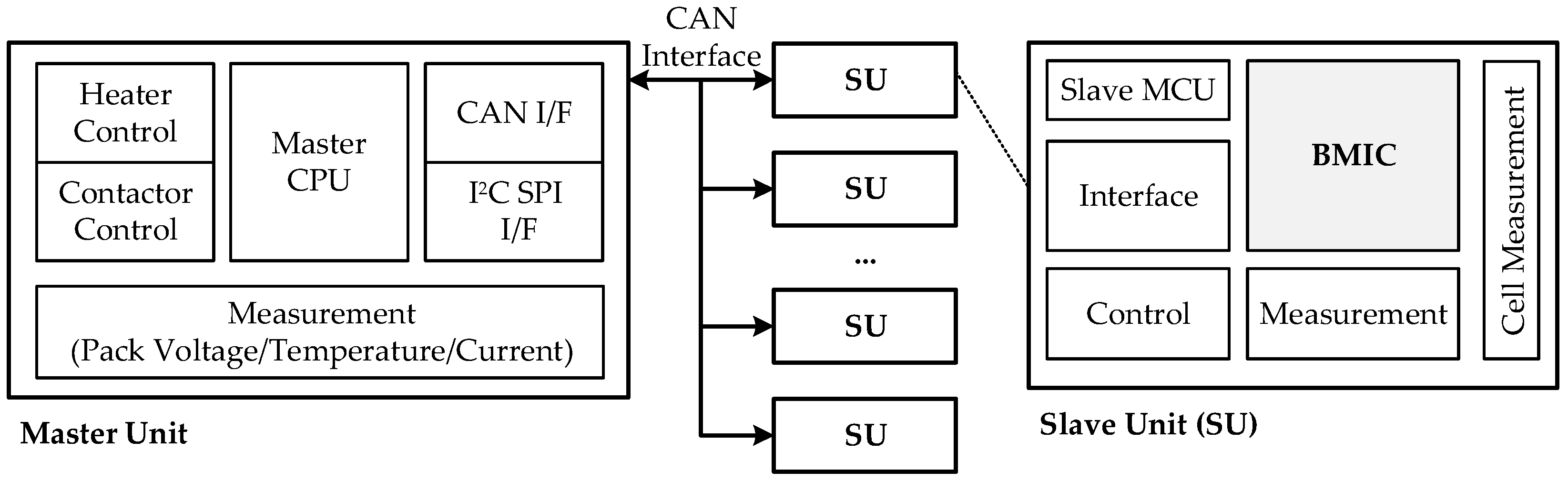
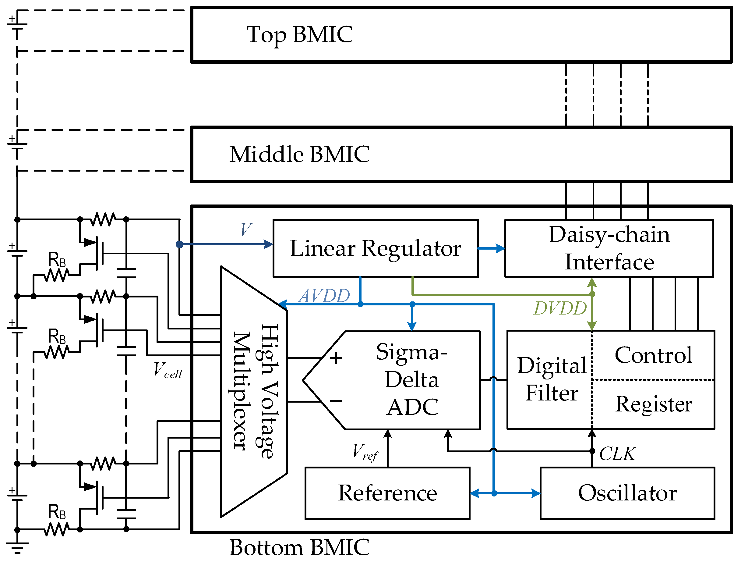
:1. Introduction
2. Principles of the Proposed BGR
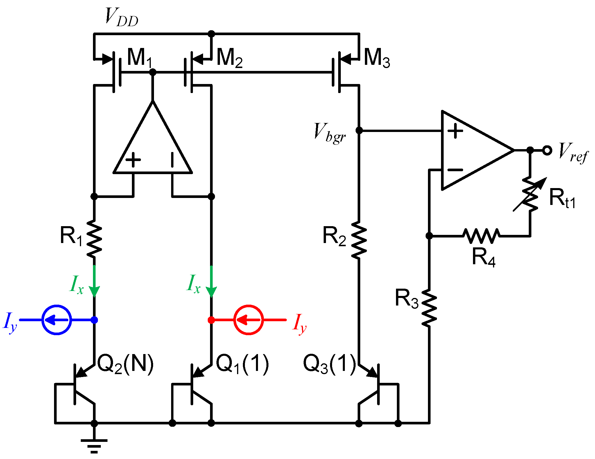
2.1. Basic BGR Topologies
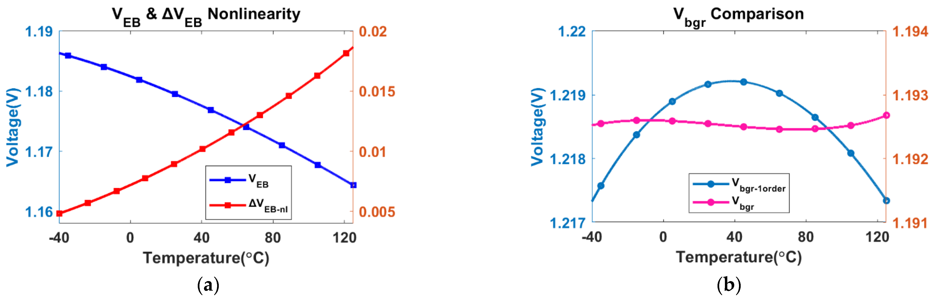
2.2. Insertion of Nonlinear Compensation in ΔVEB
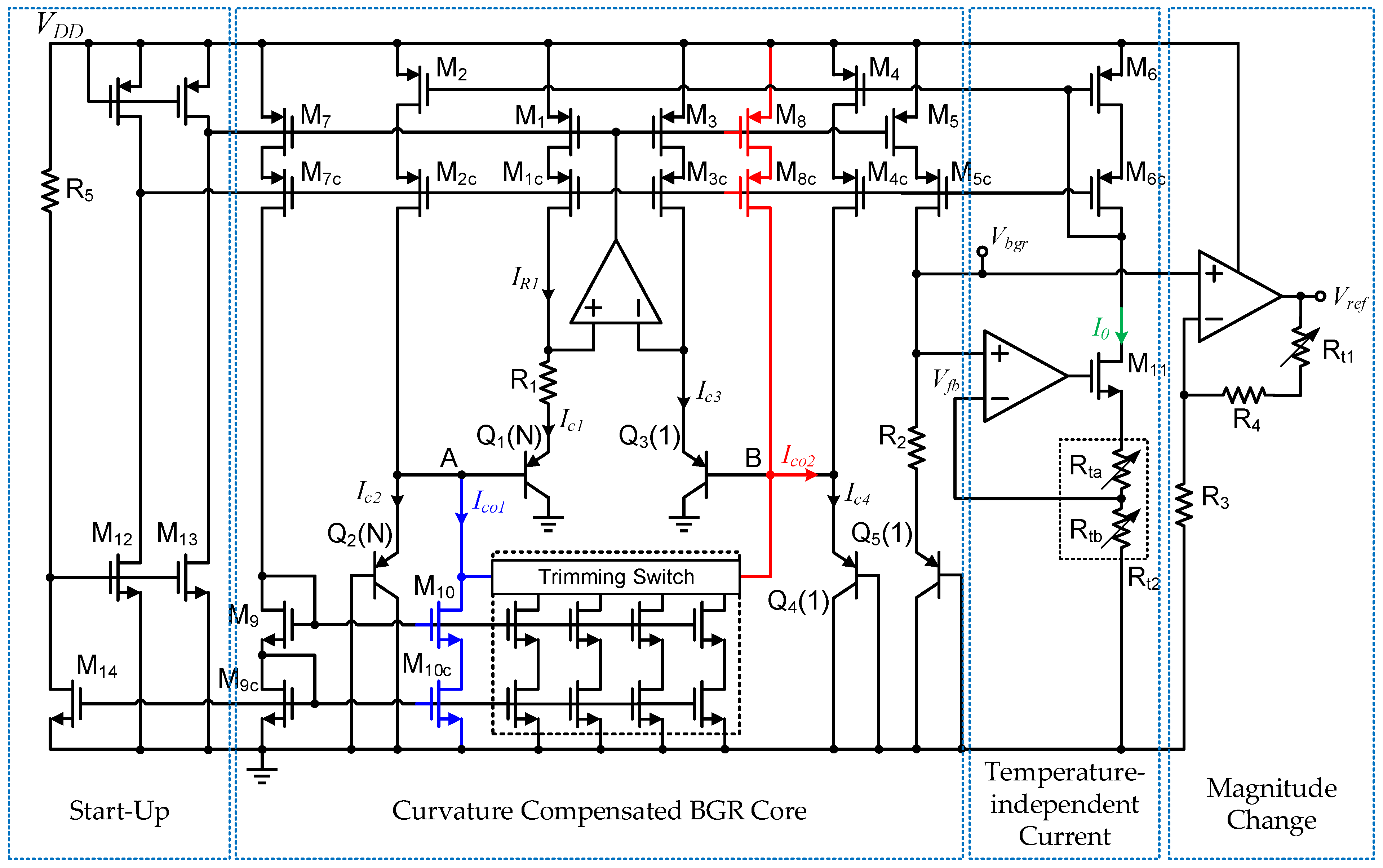
2.3. Implementation of the Proposed Circuit
2.4. Process Variations and Trimming
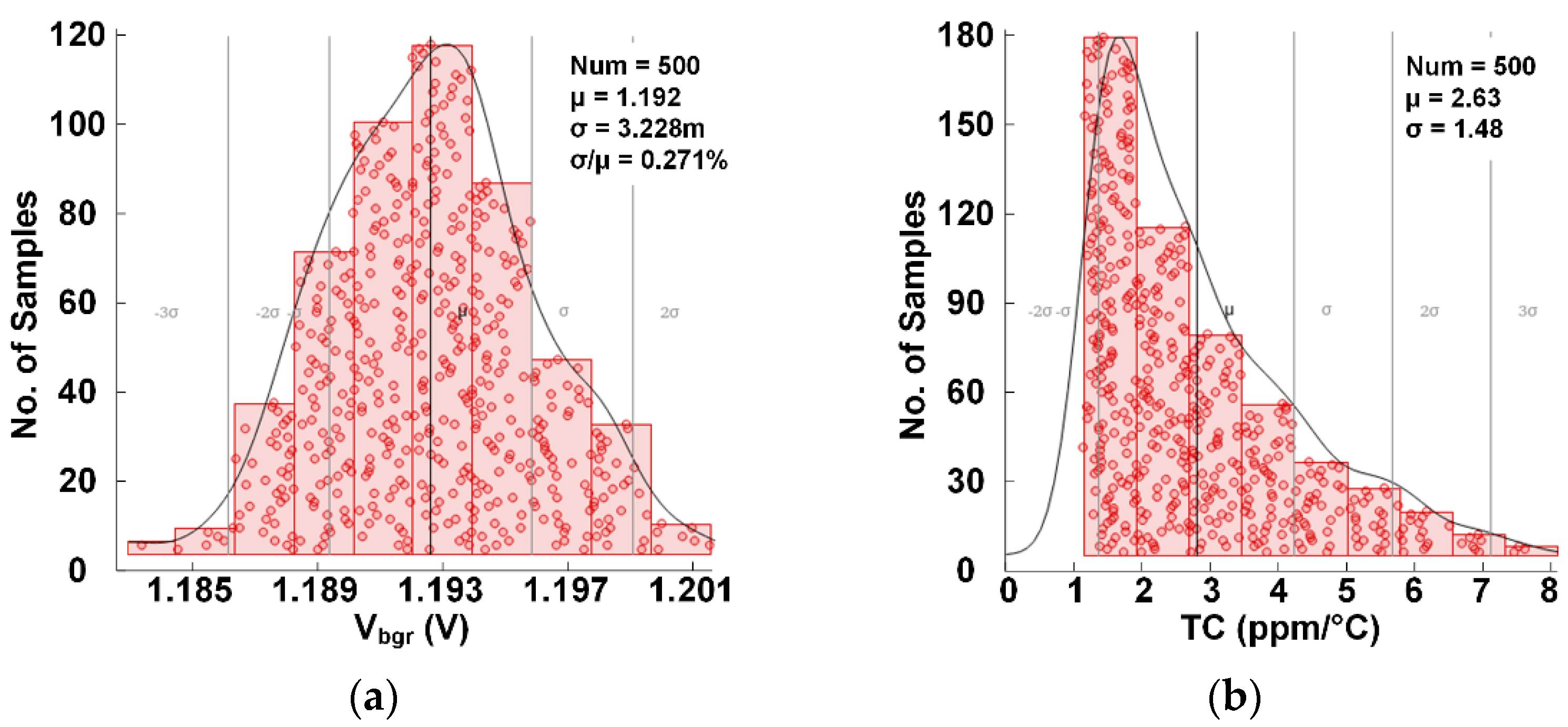
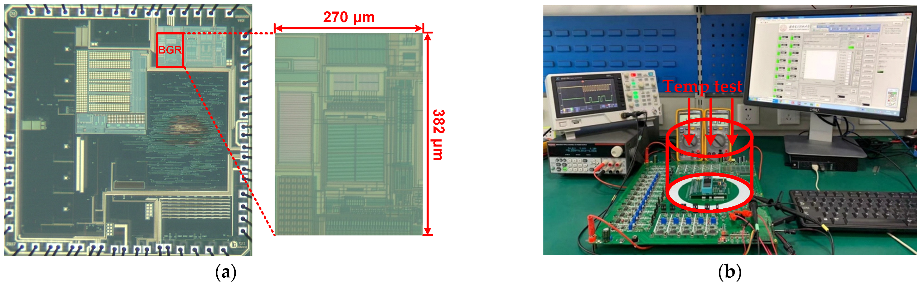
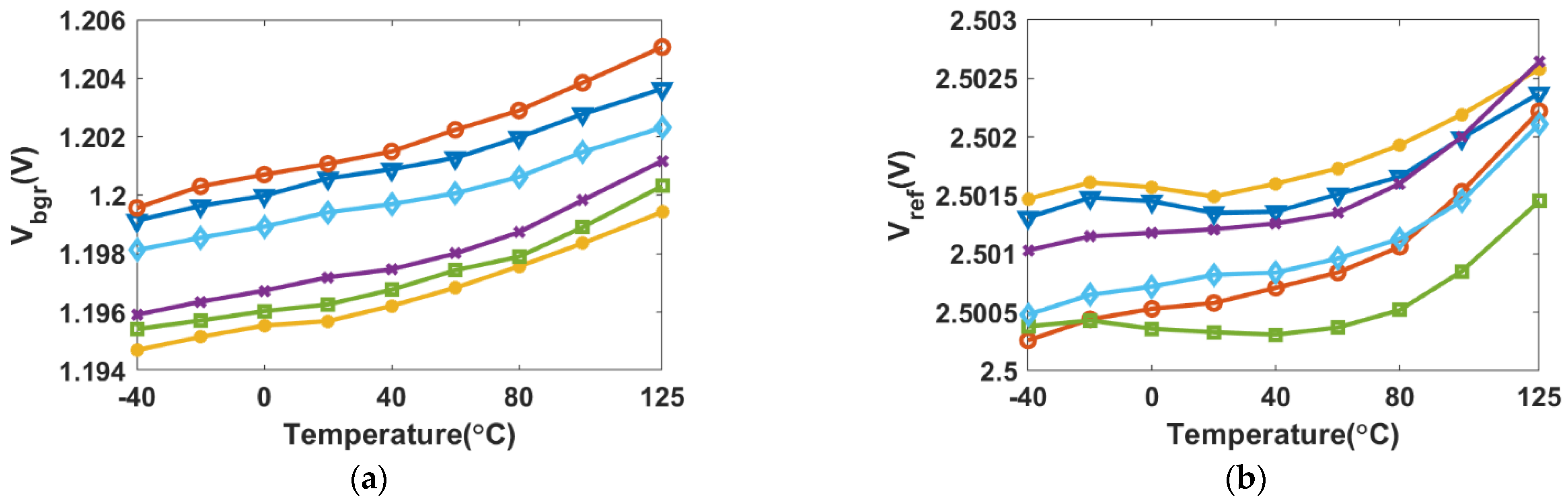
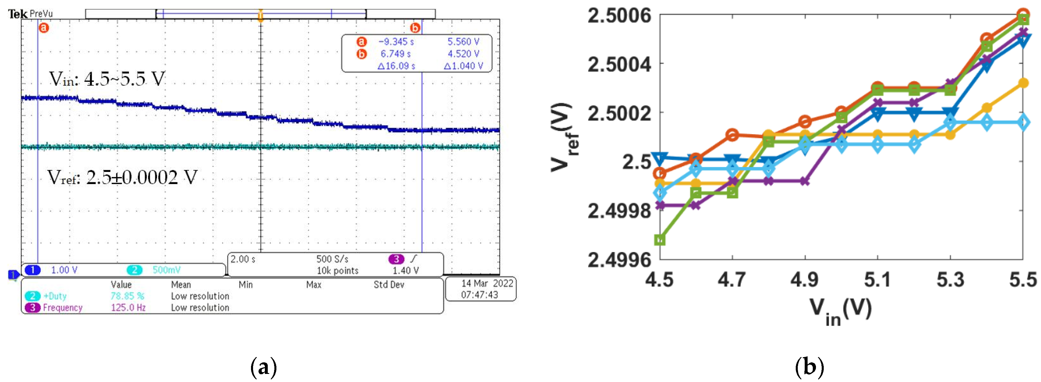
3. Experimental Results
4. Conclusions
Author Contributions
Funding
Conflicts of Interest
References
- Kadirvel, K.; Carpenter, J.; Huynh, P.; Ross, J.M.; Shoemaker, R.; Lum-Shue-Chan, B. A Stackable, 6-Cell, Li-Ion, Battery Management IC for Electric Vehicles With 13, 12-bit ΣΔ ADCs, Cell Balancing, and Direct-Connect Current-Mode Communications. IEEE J. Solid-State Circuits 2014, 49, 928–934. [Google Scholar] [CrossRef]
- Vulligaddala, V.B.; Vernekar, S.; Singamla, S.; Adusumalli, R.K.; Ele, V.; Brandl, M.; Srinivas, M.B. A 7-Cell, Stackable, Li-Ion Monitoring and Active/Passive Balancing IC With In-Built Cell Balancing Switches for Electric and Hybrid Vehicles. IEEE Trans. Ind. Inform. 2020, 16, 3335–3344. [Google Scholar] [CrossRef]
- Chen, D.; Cui, X.; Zhang, Q.; Li, D.; Cheng, W.; Fei, C.; Yang, Y. A Survey on Analog-to-Digital Converter Integrated Circuits for Miniaturized High Resolution Ultrasonic Imaging System. Micromachines 2021, 13, 114. [Google Scholar] [CrossRef] [PubMed]
- Zhang, C.; Gallichan, R.; Budgett, D.M.; McCormick, D. A Capacitive Pressure Sensor Interface IC with Wireless Power and Data Transfer. Micromachines 2020, 11, 897. [Google Scholar] [CrossRef] [PubMed]
- Abarca, A.; Theuwissen, A. In-Pixel Temperature Sensors with an Accuracy of ±0.25 °C, a 3σ Variation of ±0.7 °C in the Spatial Domain and a 3σ Variation of ±1 °C in the Temporal Domain. Micromachines 2020, 11, 665. [Google Scholar] [CrossRef]
- Kuijk, K.E. A precision reference voltage source. IEEE J. Solid-State Circuits 1973, 8, 222–226. [Google Scholar] [CrossRef]
- Banba, H.; Shiga, H.; Umezawa, A.; Miyaba, T.; Tanzawa, T.; Atsumi, S.; Sakui, K. A CMOS bandgap reference circuit with sub-1-V operation. IEEE J. Solid-State Circuits 1999, 34, 670–674. [Google Scholar] [CrossRef] [Green Version]
- Perry, R.T.; Lewis, S.H.; Brokaw, A.P.; Viswanathan, T.R. A 1.4V supply CMOS fractional bandgap reference. IEEE J. Solid-State Circuits 2007, 42, 2180–2186. [Google Scholar] [CrossRef]
- Lam, Y.H.; Ki, W.H. CMOS bandgap references with self-biased symmetrically matched current-voltage mirror and extension of sub-1-V design. IEEE Trans. Very Large Scale Integr. (VLSI) Syst. 2010, 18, 857–865. [Google Scholar] [CrossRef]
- Liu, Y.; Zhan, C.; Wang, L. An ultralow power subthreshold CMOS voltage reference without requiring resistors or BJTs. IEEE Trans. Very Large Scale Integr. (VLSI) Syst. 2018, 26, 201–205. [Google Scholar] [CrossRef]
- Liu, Y.; Zhan, C.; Wang, L.; Tang, J.; Wang, G. A 0.4-V wide temperature range all-MOSFET subthreshold voltage reference with 0.027%/V line sensitivity. IEEE Trans. Circuits Syst. II Exp. Briefs 2018, 65, 969–973. [Google Scholar] [CrossRef]
- Nagulapalli, K.; Palani, R.K.; Bhagavatula, S. A 24.4 ppm/°C voltage mode bandgap reference with a 1.05V supply. IEEE Trans. Circuits Syst. II Exp. Briefs 2021, 68, 1088–1092. [Google Scholar] [CrossRef]
- Duan, Q.; Roh, J. A 1.2-V 4.2-ppm/°C high-order curvature- compensated CMOS bandgap reference. IEEE Trans. Circuits Syst. I Reg. Pap. 2015, 62, 662–670. [Google Scholar] [CrossRef]
- Hunter, B.L.; Matthews, W.E. A ± 3 ppm/°C single-trim switched capacitor bandgap reference for battery monitoring applications. IEEE Trans. Circuits Syst. I Reg. Pap. 2017, 64, 777–786. [Google Scholar] [CrossRef]
- Vulligaddala, V.B.; Adusumalli, R.; Singamala, S.; Srinivas, M.B. A digitally calibrated bandgap reference with 0.06% error for low-side current sensing application. IEEE J. Solid-State Circuits 2018, 53, 2951–2957. [Google Scholar] [CrossRef]
- Zhu, G.; Yang, Y.; Zhang, Q. A 4.6-ppm/°C high-order curvature compensated bandgap reference for BMIC. IEEE Trans. Circuits Syst. II Exp. Briefs 2019, 66, 1492–1496. [Google Scholar] [CrossRef]
- Liu, X.; Liang, S.; Liu, W.; Sun, P. A 2.5 ppm/°C voltage reference combining traditional BGR and ZTC MOSFET high-order curvature compensation. IEEE Trans. Circuits Syst. II Exp. Briefs 2021, 68, 1093–1097. [Google Scholar] [CrossRef]
- Wang, S.; Mok, P.K.T. An 18-nA ultra-low-current resistor-less bandgap reference for 2.8 V–4.5 V high voltage supply Li-Ion-battery-based LSIs. IEEE Trans. Circuits Syst. II Exp. Briefs 2020, 67, 2382–2386. [Google Scholar] [CrossRef]
- Kamath, U.; Cullen, E.; Yu, T.; Jennings, J.; Wu, S.; Lim, P.; Farley, B.; Staszewski, R.B. A 1-V bandgap reference in 7-nm FinFET with a programmable temperature coefficient and inaccuracy of ±0.2% from −45 °C to 125 °C. IEEE J. Solid-State Circuits 2019, 54, 1830–1840. [Google Scholar] [CrossRef]
- Lee, K.K.; Lande, T.S.; Häfliger, P.D. A sub-μW bandgap reference circuit with an inherent curvature-compensation property. IEEE Trans. Circuits Syst. I Reg. Pap. 2015, 62, 1–9. [Google Scholar] [CrossRef]
- Ma, B.; Yu, F. A novel 1.2–V 4.5-ppm/°C curvature-compensated CMOS bandgap reference. IEEE Trans. Circuits Syst. I Reg. Pap. 2014, 61, 1026–1035. [Google Scholar] [CrossRef]
- Ge, G.; Zhang, C.; Hoogzaad, G.; Makinwa, K.A.A. A single-trim CMOS bandgap reference with a 3-s inaccuracy of 0.15% from −40 °C to 125 °C. IEEE J. Solid-State Circuits 2011, 46, 2693–2701. [Google Scholar] [CrossRef]
- Tsividis, Y.P. Accurate analysis of temperature effects in IC-VBE characteristics with application to bandgap reference sources. IEEE J. Solid-State Circuits 1980, 15, 1076–1084. [Google Scholar] [CrossRef]
- Filanovsky, I.M.; Chan, Y.F. BiCMOS cascaded bandgap voltage reference. In Proceedings of the 39th IEEE Midwest Symposium Circuits and Systems, Ames, IA, USA, 21 August 1996; pp. 943–946. [Google Scholar]


| [17] TCASII | [16] TCASII | [14] TCASI | [13] TCASI | [21] TCASI | [22] JSSC | This Work | |
|---|---|---|---|---|---|---|---|
| Tech (μm) | 0.18 | 0.18 | 0.18 | 0.13 | 0.18 | 0.16 | 0.18 |
| Year | 2021 | 2019 | 2017 | 2015 | 2014 | 2011 | 2022 |
| Supply Voltage (V) | 1.2–2.4 | 3.5–5 | 5.2 | 1.2 | 1.2 | 1.8 | 5 |
| Reference Voltage (V) | 0.628 | 3.11 | 3.65 | 0.735 | 0.767 | 1.088 | 2.5 |
| Temperature Range (°C) | −40~120 | −40~130 | −40~110 | −40~120 | −40~120 | −40~125 | −40~125 |
| TC Range (ppm/°C) | 2.5~5 | 4.6~7.6 | ±3@3σ | 9.3 | 4.9 | 5~12 | 2.56~4.75 |
| LS (%/V) | 0.03 | 0.031 | N/A | N/A | 0.54 | 0.48 | 0.023 |
| Power (μA) | 64.2 | 108 | 750 | 120 | 36 | 55 | 53 |
| PSRR (dB) | −91.4 * | −92 * | −127 | N/A | −80 | −74 | −84 * |
| Area (mm2) | 0.024 | 0.223 | 0.28 | 0.063 | 0.036 | 0.12 | 0.103 |
Publisher’s Note: MDPI stays neutral with regard to jurisdictional claims in published maps and institutional affiliations. |
© 2022 by the authors. Licensee MDPI, Basel, Switzerland. This article is an open access article distributed under the terms and conditions of the Creative Commons Attribution (CC BY) license (https://creativecommons.org/licenses/by/4.0/).
Share and Cite
Zhu, G.; Fu, Z.; Liu, T.; Zhang, Q.; Yang, Y. A 2.5 V, 2.56 ppm/°C Curvature-Compensated Bandgap Reference for High-Precision Monitoring Applications. Micromachines 2022, 13, 465. https://doi.org/10.3390/mi13030465
Zhu G, Fu Z, Liu T, Zhang Q, Yang Y. A 2.5 V, 2.56 ppm/°C Curvature-Compensated Bandgap Reference for High-Precision Monitoring Applications. Micromachines. 2022; 13(3):465. https://doi.org/10.3390/mi13030465
Chicago/Turabian StyleZhu, Guangqian, Zhaoshu Fu, Tingting Liu, Qidong Zhang, and Yintang Yang. 2022. "A 2.5 V, 2.56 ppm/°C Curvature-Compensated Bandgap Reference for High-Precision Monitoring Applications" Micromachines 13, no. 3: 465. https://doi.org/10.3390/mi13030465
APA StyleZhu, G., Fu, Z., Liu, T., Zhang, Q., & Yang, Y. (2022). A 2.5 V, 2.56 ppm/°C Curvature-Compensated Bandgap Reference for High-Precision Monitoring Applications. Micromachines, 13(3), 465. https://doi.org/10.3390/mi13030465