
An Endpoint Detection System for Ion Beam Etching Using Optical Emission Spectroscopy


Abstract
:1. Introduction
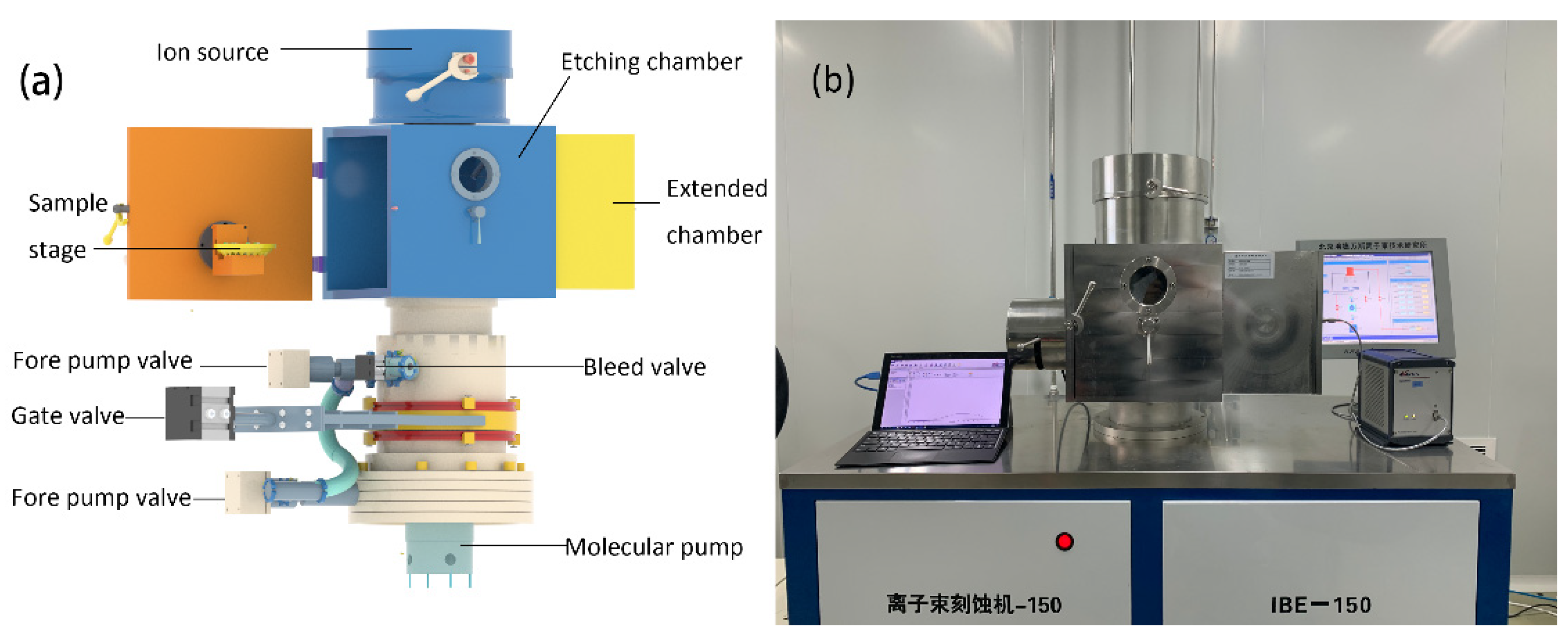
2. System Design
2.1. Overall Structure
2.2. Expansion Chamber
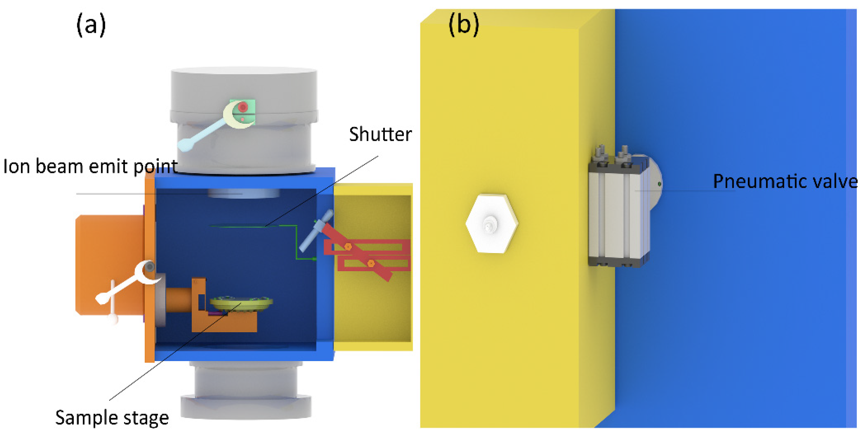
2.3. Shutter
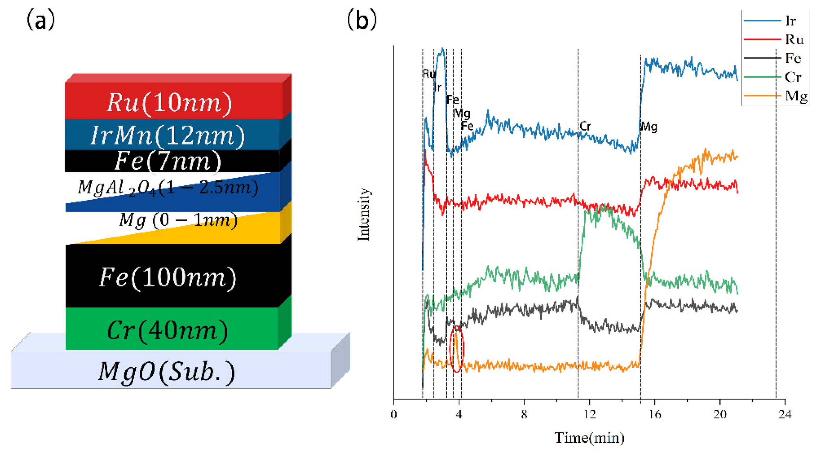
3. Results
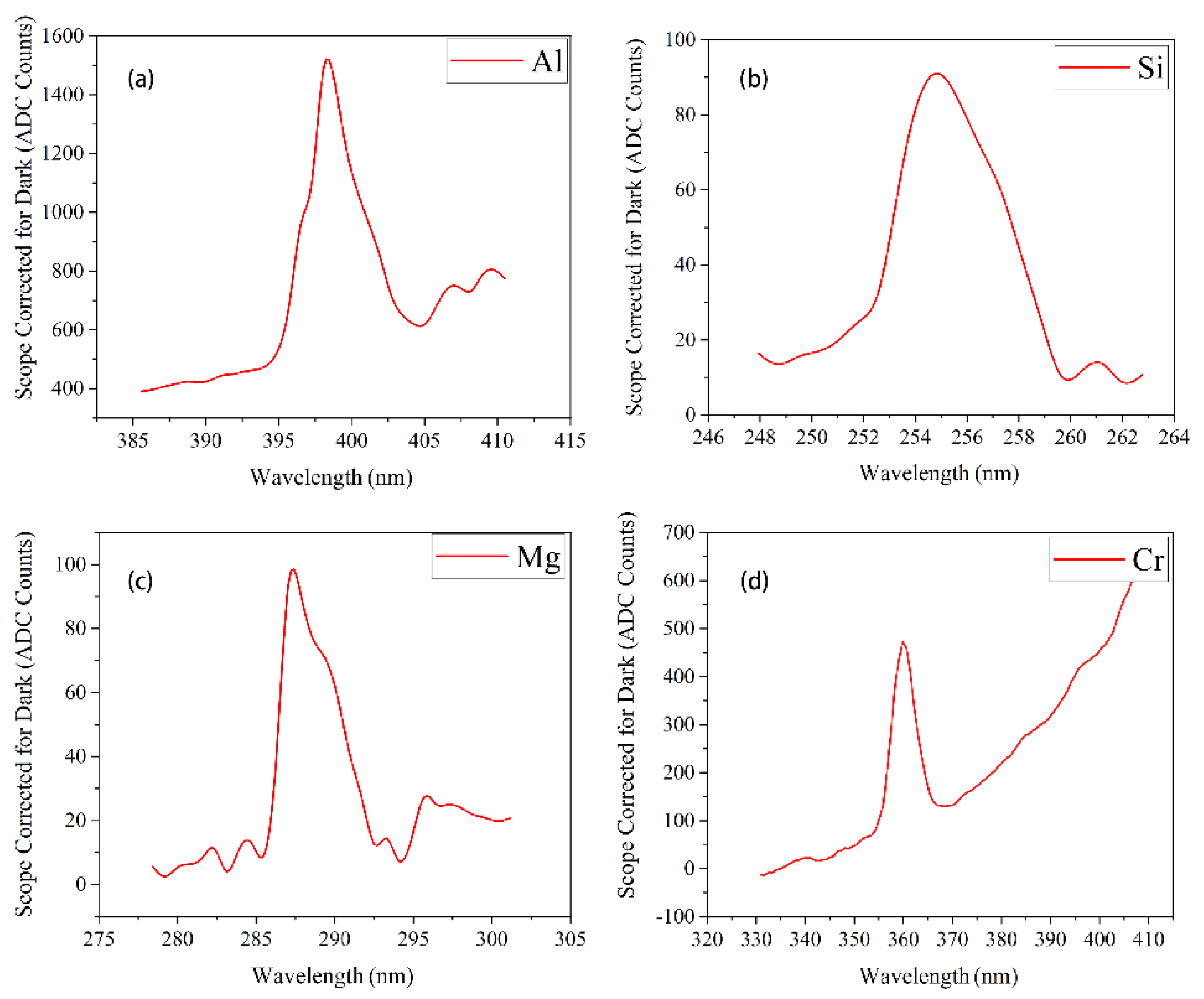
3.1. Simple Substance
3.2. The Setting of Optical Detector
4. Performance
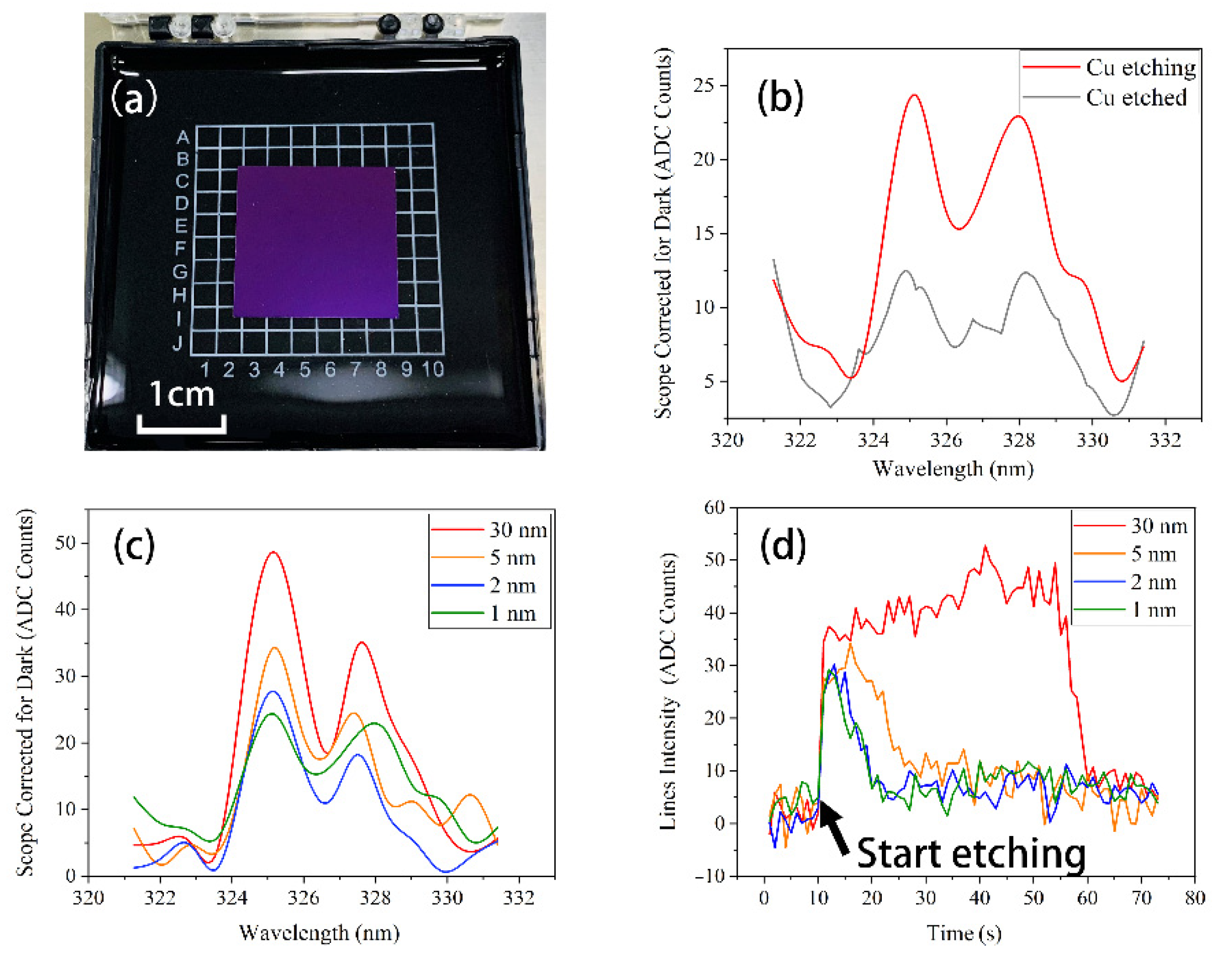
4.1. Detection Limit
4.2. Application
5. Conclusions
Supplementary Materials
Author Contributions
Funding
Conflicts of Interest
References
- Glöersen, P.G. Ion-beam etching. J. Vac. Sci. Technol. 1975, 12, 28–35. [Google Scholar] [CrossRef]
- Desbiolles, B.; Bertsch, A.; Renaud, P. Ion beam etching redeposition for 3D multimaterial nanostructure manufacturing. Microsyst. Nanoeng. 2019, 5, 1–8. [Google Scholar] [CrossRef] [PubMed] [Green Version]
- Nagase, T.; Gamo, K.; Kubota, T.; Mashiko, S. Direct fabrication of nano-gap electrodes by focused ion beam etching. Thin Solid Films 2006, 499, 279–284. [Google Scholar] [CrossRef]
- Qian, H.; Zhou, W.; Miao, J.; Lim, L.E.; Zeng, X. Fabrication of Si microstructures using focused ion beam implantation and reactive ion etching. J. Micromech. Microeng. 2008, 18, 035003. [Google Scholar] [CrossRef]
- Youtsey, C.; Grundbacher, R.; Panepucci, R.; Adesida, I.; Caneau, C. Characterization of chemically assisted ion beam etching of InP. J. Vac. Sci. Technol. B Microelectron. Nanometer. Struct. Process. Meas. Phenom. 1994, 12, 3317–3321. [Google Scholar] [CrossRef]
- Sugiura, K.; Takahashi, S.; Amano, M.; Kajiyama, T.; Iwayama, M.; Asao, Y.; Shimomura, N.; Kishi, T.; Ikegawa, S.; Yoda, H.; et al. Ion beam etching technology for high-density spin transfer torque magnetic random access memory. Jpn. J. Appl. Phys. 2009, 48, 08HD02. [Google Scholar] [CrossRef]
- Peng, X.; Wakeham, S.; Morrone, A.; Axdal, S.; Feldbaum, M.; Hwu, J.; Boonstra, T.; Chen, Y.; Ding, J. Towards the sub-50 nm magnetic device definition: Ion beam etching (IBE) vs plasma-based etching. Vacuum 2009, 83, 1007–1013. [Google Scholar] [CrossRef]
- Bunyard, G.B.; Raby, B.A. Plasma Process-Development and Monitoring via Mass-Spectrometry. Solid State Technol. 1977, 20, 53–57. [Google Scholar]
- Kanoh, M.; Yamage, M.; Takada, H. End-point detection of reactive ion etching by plasma impedance monitoring. Jpn. J. Appl. Phys. 2001, 40, 1457. [Google Scholar] [CrossRef]
- McMillin, B.K.; Dassapa, F.C. Method and apparatus for etch endpoint detection. U.S. Patent 7053994, 30 May 2006. [Google Scholar]
- Lu, C.; Dorian, M.; Tabei, M.; Elsea, A. End point detection in ion milling processes by sputter-induced optical emission spectroscopy. J. Vac. Sci. Technol. A Vac. Surf. Films 1984, 2, 481–484. [Google Scholar] [CrossRef]
- Gu, J.M.; Thadesar, P.A.; Dembla, A.; Bakir, M.S.; May, G.S.; Hong, S.J. Endpoint detection in low open area TSV fabrication using optical emission spectroscopy. IEEE Trans. Compon. Packag. Manuf. Technol. 2014, 4, 1251–1260. [Google Scholar]
- Lee, J.; Jeon, M.; Cho, G.; Yim, H.; Chang, S.; Kim, K.; Devre, M.; Johnson, D.; Sasserath, J.; Pearton, S. Development of advanced plasma process with an optical emission spectroscopy-based end-point technique for etching of AlGaAs over GaAs in manufacture of heterojunction bipolar transistors. Solid State Electron. 2002, 46, 773–775. [Google Scholar] [CrossRef]
- Dreeskornfeld, L.; Segler, R.; Haindl, G.; Wehmeyer, O.; Rahn, S.; Majkova, E.; Kleineberg, U.; Heinzmann, U.; Hudek, P.; Kostic, I. Reactive ion etching with end point detection of microstructured Mo/Si multilayers by optical emission spectroscopy. Microelectron. Eng. 2000, 54, 303–314. [Google Scholar] [CrossRef]
- Pearton, S.; Ren, F.; Abernathy, C.; Constantine, C. Optical emission end point detection for via hole etching in InP and GaAs power device structures. Mater. Sci. Eng. B 1994, 23, 36–40. [Google Scholar] [CrossRef]
- Lipschultz, B.; Hutchinson, I.; LaBombard, B.; Wan, A. Electric probes in plasmas. J. Vac. Sci. Technol. A Vac. Surf. Films 1986, 4, 1810–1816. [Google Scholar] [CrossRef] [Green Version]
- Gokan, H.; Esho, S. Pattern fabrication by oblique incidence ion-beam etching. J. Vac. Sci. Technol. 1981, 18, 23–27. [Google Scholar] [CrossRef]


| Elements | Spectroscopic Notation | Upper Energy Level | Lower Energy Level | Emitted Wavelength |
|---|---|---|---|---|
| Al | Al I | 396.152 | ||
| Al | Al III | 398.014 | ||
| Cu | Cu I | 324.754, 327.395 | ||
| Mg | Mg I | 285.2127 | ||
| Si | Si III | 254.609 | ||
| Cr | Cr I | 359.350, 360.534 | ||
| Ir | Ir I | 403.376 | ||
| Ru | Ru I | 372.803 | ||
| Fe | Fe I | 374.826 |
| Angles | 30° | 40° | 50° | 60° |
|---|---|---|---|---|
| Average (Intensity) | 218.80 | 262.60 | 378.10 | 92.47 |
| Distances | 10.8 cm | 11.3 cm | 12.8 cm | 14.3 cm |
|---|---|---|---|---|
| Average (Intensity) | 355.09 | 321.60 | 260.18 | 225.17 |
Publisher’s Note: MDPI stays neutral with regard to jurisdictional claims in published maps and institutional affiliations. |
© 2022 by the authors. Licensee MDPI, Basel, Switzerland. This article is an open access article distributed under the terms and conditions of the Creative Commons Attribution (CC BY) license (https://creativecommons.org/licenses/by/4.0/).
Share and Cite
Zhang, J.; Luo, J.; Zou, X.; Chen, J. An Endpoint Detection System for Ion Beam Etching Using Optical Emission Spectroscopy. Micromachines 2022, 13, 259. https://doi.org/10.3390/mi13020259
Zhang J, Luo J, Zou X, Chen J. An Endpoint Detection System for Ion Beam Etching Using Optical Emission Spectroscopy. Micromachines. 2022; 13(2):259. https://doi.org/10.3390/mi13020259
Chicago/Turabian StyleZhang, Junjie, Jiahui Luo, Xudong Zou, and Jiamin Chen. 2022. "An Endpoint Detection System for Ion Beam Etching Using Optical Emission Spectroscopy" Micromachines 13, no. 2: 259. https://doi.org/10.3390/mi13020259
APA StyleZhang, J., Luo, J., Zou, X., & Chen, J. (2022). An Endpoint Detection System for Ion Beam Etching Using Optical Emission Spectroscopy. Micromachines, 13(2), 259. https://doi.org/10.3390/mi13020259