Article

SiC Heterojunction Trench MOSFET with a Buried P-Type Pillar for the Low Gate-Drain Charge and Switching Loss

Chongqing Engineering Laboratory of High Performance Integrated Circuits, School of Microelectronics and Communication Engineering, Chongqing University, Chongqing 400044, China
*
Author to whom correspondence should be addressed.
Micromachines 2022, 13(2), 248; https://doi.org/10.3390/mi13020248
Submission received: 16 January 2022 / Revised: 30 January 2022 / Accepted: 31 January 2022 / Published: 1 February 2022

Abstract

:
A novel Silicon-Carbide heterojunction U-MOSFET embedded a P-type pillar buried in the drift layer (BP-TMOS) is proposed and simulated in this study. When functioning in the on state, the merged heterojunction structure will control the parasitic body diode, and the switching loss will decrease. Moreover, to lighten the electric field on the gate oxide corner, a high-doped L-shaped P+ layer near the heterojunction beneath the gate oxide was introduced; thus, the gate oxide reliability improved. A p-type pillar is introduced in the drift layer. The p-type pillar can assistant the drift layer to deplete. Thus, the specific on-resistance for BP-TMOS can be reduced with an increase in the N-drift region’s doping concentration. Compared to the traditional SiC MOSFET (C-TMOS), the specific on-resistance decreased by 20.4%, and the breakdown voltage increased by 53.7% for BP-TMOS, respectively. Meanwhile the device exhibits a 55% decrease and a 69.7% decrease for the switching loss and gate to drain charge.

1. Introduction

Over the years, the wide band-gap material has become a new research topic in the power devices. Silicon–carbide devices is a major type used in the power systems. The low on-state resistance, higher power density, increased high work frequency, and the widely forbidden band all stand out [1,2,3]. The small size and high reliability of the SiC MOSFET are both necessary to minish power dissipation and increase the efficiency. To avoid the aged deterioration effect, when the SiC MOSFET is used in the power system, usually paralleled with a Schottky barrier diode (SBD) [4,5,6,7], it may cause more energy dissipation and undesirable stray inductances. In order to obtain the optimised the reverse recovery performance and reduce switching loss, several papers have proposed several structures, for example, using a SBD paralleled with the SiC trench MOSFET [8,9,10,11,12]. In addition, in the trench SiC MOSFET, the gate oxide corner reliability is also an issue of interest. Under the trench gate, surrounding a highly doped P+ layer is an effective method.
Compared to the SiC SBD, two types of poly-silicon/SiC formed the heterojunction diode, which have better performance on the third quadrant. In this paper, the novel structure that buried a P-type pillar in drift layer has been researched. In addition to the optimised reverse recovery performance and the reduced the switching loss from the Heterojunction diode (HJD) in the drift region, the assist depletion effect from the P-pillar can bring a better balance among the specific on-resistance (Ron,sp) and the breakdown voltage (BV). The dynamic and static performances of the proposed structure have been carefully investigated.

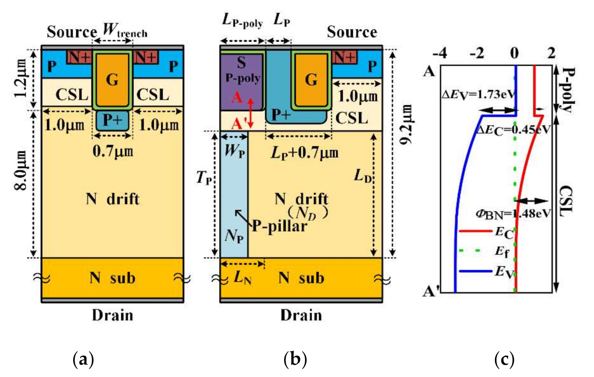
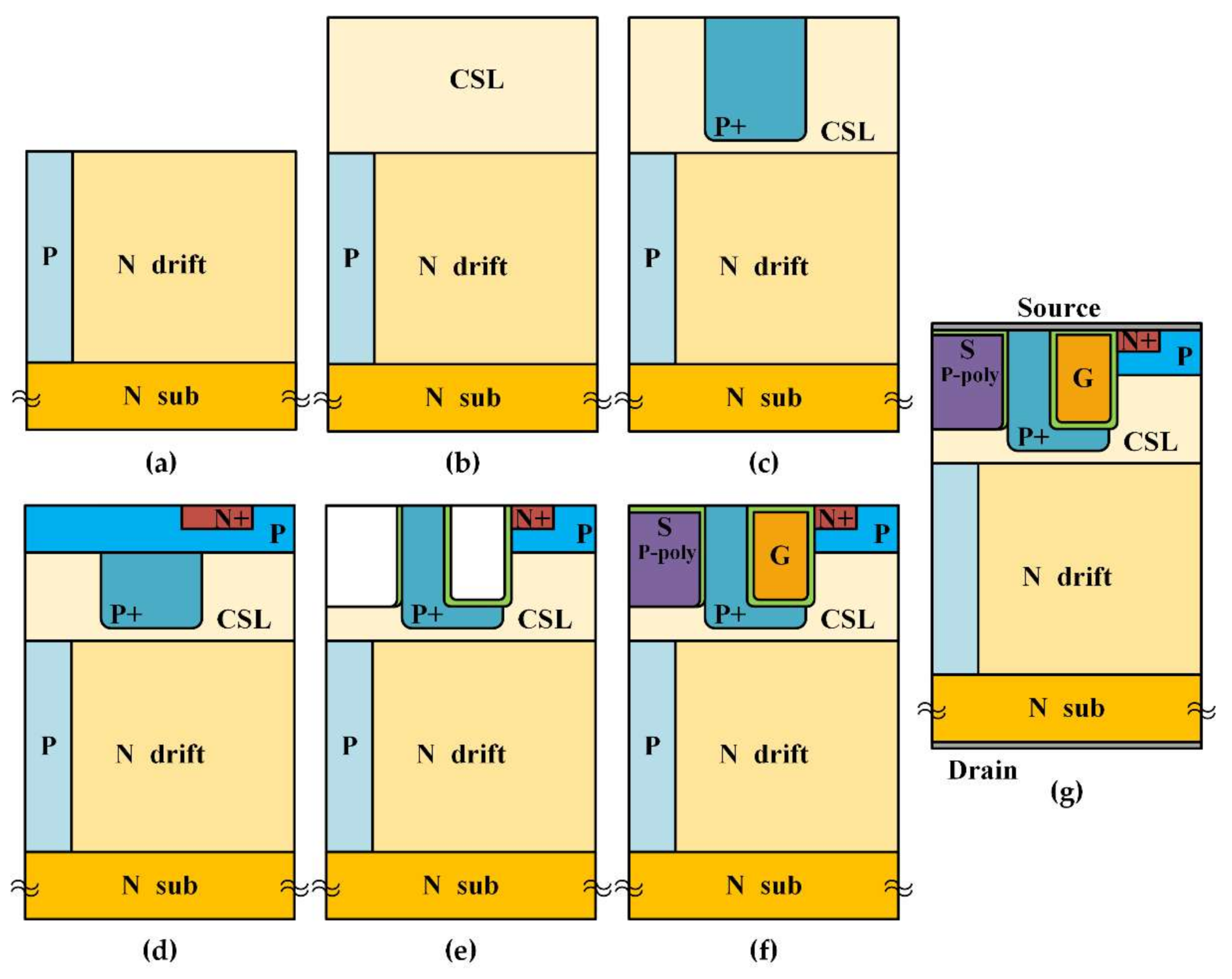
2. Device Structure and Mechanism

Figure 1a,b show the structures of the BP-TMOS that buried a P-type pillar and the traditional SiC MOSFET(C-TMOS). The energy band along the poly-silicon/SiC in the BP-TMOS is also shown in Figure 1c. In comaprison to the traditional one, BP-TMOS also has a heterojuction structure, which is composed of the poly-silicon/SiC. The heterojuction structure has a conduction band of 0.45 eV and valence band of 1.73 eV, respectively. An electron barrier height ΦBN (about 1.48 eV) is caused by conduction band EC and the Fermi-band Ef. When the device is in a forward state, the height of this barrier will result in a smaller forward voltage (VF). Conversely, in a reverse position, the breakdown voltage BV is enhanced. Beneath the gate oxide and near the heterojunction, using a highly doped L-shaped P+ region reduced the gate oxide maximum electric field and improved the gate oxide layer’s reliability [13,14,15]. In addition, in the drift region near the gate oxide corner, the electric field concentration can lower by the L-shaped P+ layer and narrow the overlap area between the drift layer and the gate oxide layer and, thus, can achieve a fast-switching time and a high BV. From the work mechanism, the P-type pillar will afford an assistant depletion effect. Thus, the lateral P-pillar/N-drift junction and the vertical P-base/N-drift junction consist of the total depletion in drift layer. The drift layer doping concentration can be increased. Therefore, Ron,sp can be reduced and BV can be increased at the same time.
For practice, the device was placed in a tape-out process at the interface of SiO2, and SiC introduced the traps with a uniform concentration 5 × 10¹² eV−1 cm−2. Table 1 lists the basic parameters of the two devices. In this paper, the devices were analysed by the Sentaurus TCAD tool. In a recombination process, Auger recombination, Shockley–Read–Hall (SRH), and doping-dependent methods are used, and Okuto–Crowell models are used in the electron/hole continuity equations [16]. The mobility model used Enormal, high-field velocity saturation, and incomplete ionization.

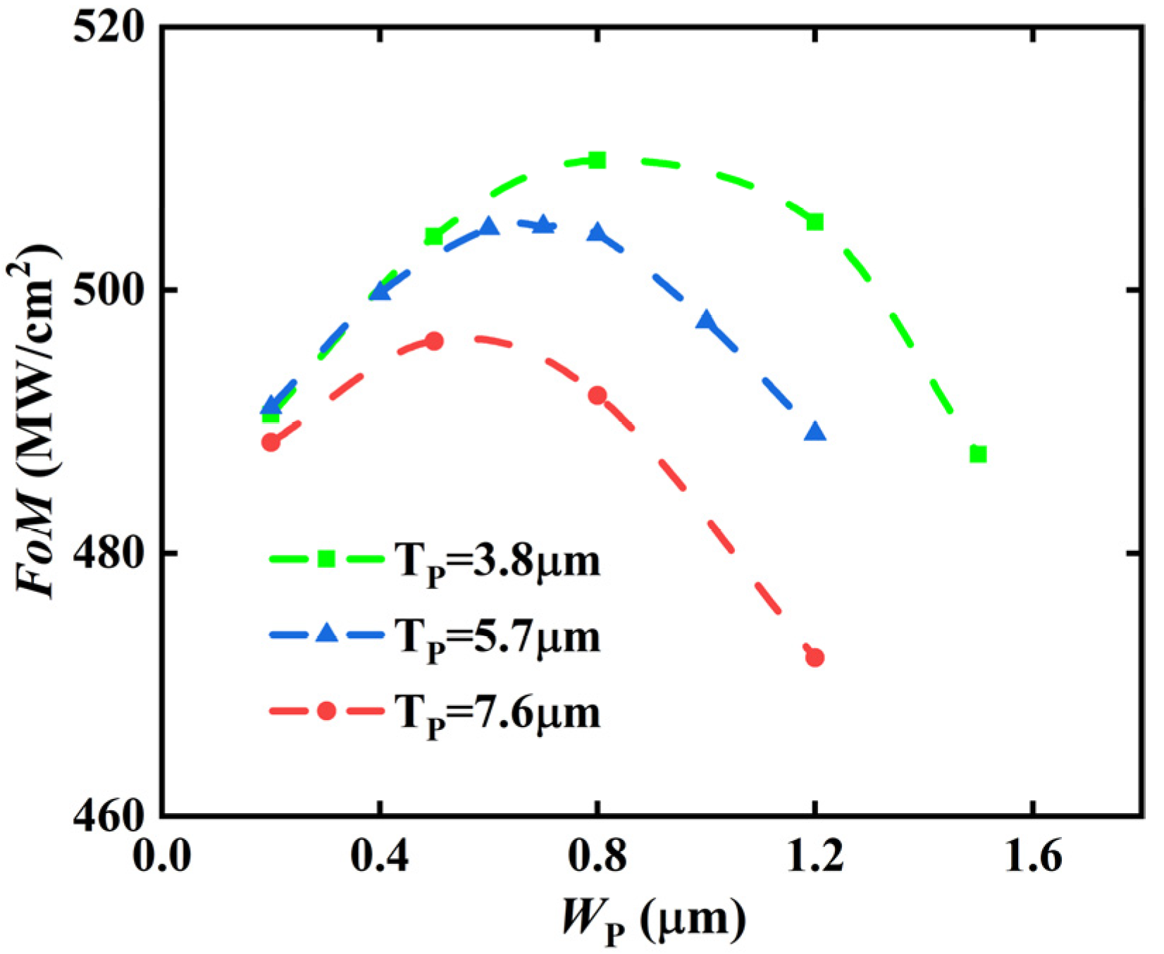
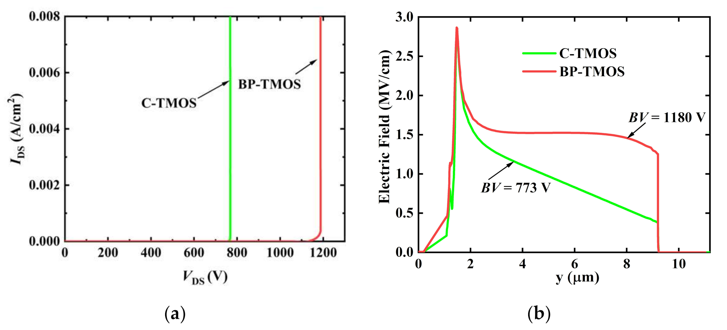
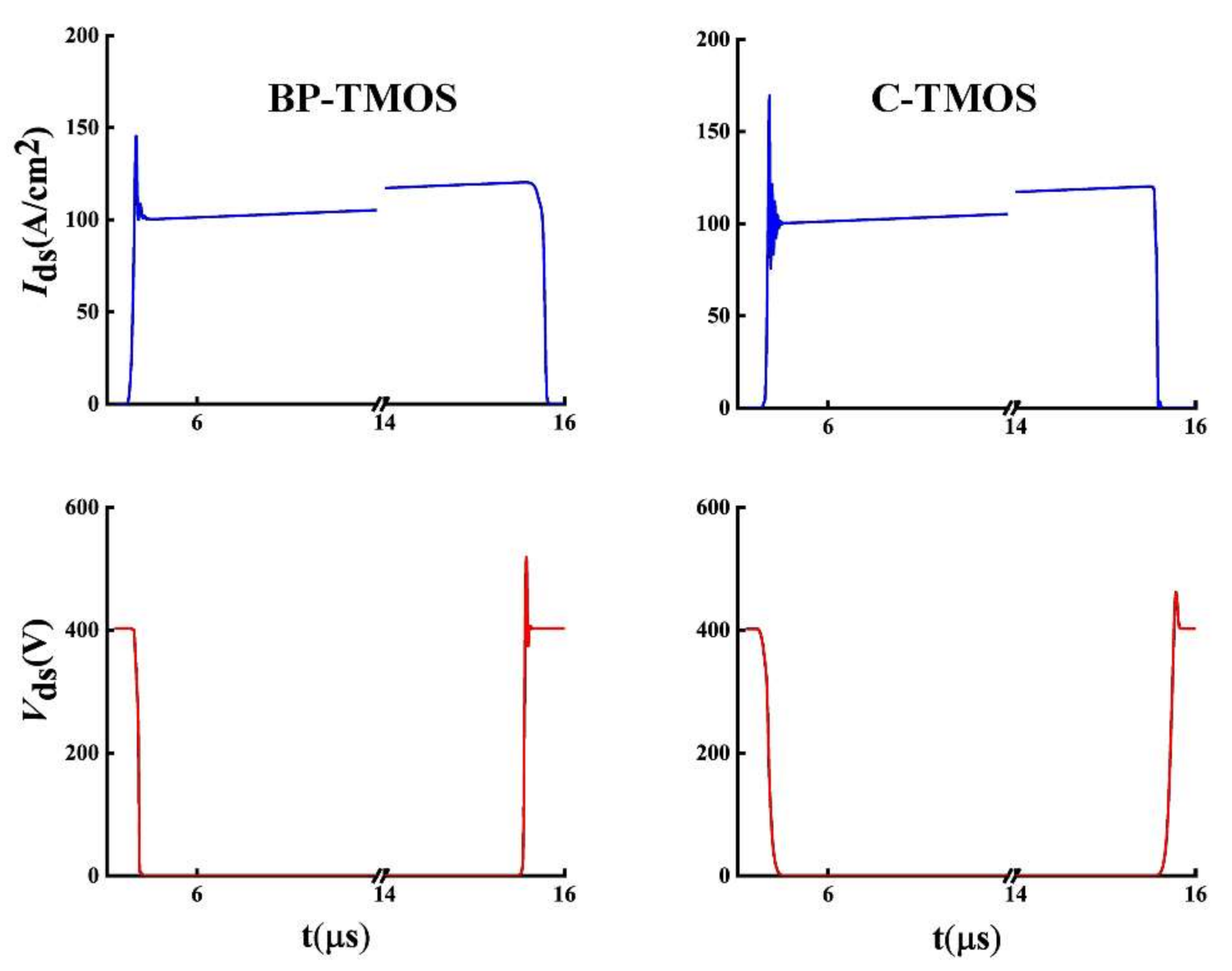
3. Results and Discussions

Figure 2 shows the FoM (Figure of Merit, BV2/Ron) with different WP and TP for the BP-TMOS. Fixing a certain TP of 3.8 μm, 5.7 μm, or 7.6 μm, FoM increases at first and then declines with an increase in WP. There is a maximum point for the FoM. The TP is chosen when it is equal to the drift thickness (LD), and WP is chosen when the largest FoM is obtained. Just as shown in Figure 2, the optimised values of WP and TP are 0.5 μm and 7.6 μm for BP-TMOS, respectively.
Figure 3 provides the off-state characteristics about the proposed one and the traditional one. Figure 3a includes the off-state I-V curves. It clearly shows that the BVs of BP-TMOS and C-TMOS are 1180 V and 773 V, respectively. The total drain-source current Ids achieves 10 μA/cm2 when considering its breakdown. Figure 3b shows the electric field distributions of BP-TMOS and C-TMOS on the vertical direction when the breakdown takes place. The electric field distribution in drift layer of BP-TMOS is uniform due to the assistant depletion effect of the P-pillar and wider P+ layer; thus, it has a higher BV.
Figure 4 provides the 2D electric field graphics of BP-TMOS and C-TMOS in the same drain voltage of 650 V. For BP-TMOS, the gate oxide corner maximum electric field (Eox) is 1.2 MV/cm, which is lower than 1.45 MV/cm for the C-TMOS. That is to say that the gate oxide reliability of BP-TMOS is better. In addition, the SiC region maximum electric field (ESiC) in BP-TMOS is also much lower, which means the premature breakdown near the P+ shielding layer is restrained for BP-TMOS, and a higher BV is, therefore, obtained as shown in Figure 3.
Figure 5 provides the devices’ electric performances with different structure parameters. Figure 5a shows the dependences on BV with different NP and ND for the BP-TMOS. It can be observed that there is a maximum point of BV for certain ND. Due to mutual depletion, a higher ND needs a higher NP to obtain the maximum BV. Figure 5b provides the optimizations of BV and Ron,sp for BP-TMOS and C-TMOS. The criteria conditions include FoM. The optimised value of ND for BP-TMOS is chosen as 1.5 × 1016 cm−3, while in C-TMOS, it is 7.5 × 1015 cm−3, and an NP of 8.1 × 1016 cm−3 was chosen. Compared to C-TMOS, BP-TMOS has a larger FoM.
Figure 6 shows the third quadrant I-V curves for C-TMOS and BP-TMOS. It is obvious that the reverse voltage (VF) of BP-TMOS is far below C-TMOS because of HJD; as a result, BP-TMOS has a small dead-time loss. Moreover, just as Figure 6b shows, when the drain hole current IdsH = 10 A/cm2, the reverse voltage (VPN) of the BP-TMOS increases to 3.4 V, while the VPN of the C-TMOS is 2.7 V. This indicated that BP-TMOS has a large turn-on voltage relative to the body diode; thus, unwanted consumption can be controlled.
Figure 7 shows the dependences between the gate voltage (Vg) and gate charge (Qg) of the devices. The active device area is set to be 1 cm2. The Qg and the gate-drain charge (Qgd) are 525 nC/cm2 and 50 nC/cm2 for BP-TMOS, respectively, which are both smaller than 775 nC/cm2 and 165 nC/cm2 of C-TMOS. This is because there is a L-shaped P+ layer in the BP-MOSFET, which reduces the overlap area between the drift region and the gate oxide.
The switching performances analysis of the two devices used mixed-mode simulation in a double-pulse test. Figure 8 shows the switching performances for the two devices. Although SiC SBD has been used when simulating C-TMOS, BP-TMOS still has a small current spike in the turn-on state compared to C-TMOS.
Figure 9 shows test circuit and switching losses. Figure 9b shows the switching loss results for the two devices. In comparison to C-TMOS, BP-TMOS has 55% decrease. The smaller Qgd charge and the introduced heterojunction structure are the pivotal elements for the low switching loss. Table 2 summarises device performances, and BP-TMOS has a better comprehensive performances.
A feasible fabrication procedure of the proposed device is provided in Figure 10. The double epitaxial layers including N drift and CSL are grown on the N substrate layer by chemical vapour deposition (CVD). The P-type layer in N drift used dose aluminium implantation. The P + shielding layer and the floating guard rings in termination region are formed simultaneously by heavy-dose aluminium implantation at 500 °C ambient temperature. After forming the P channel and N + source regions, all implants are activated at 1600 °C. The gate trench is formed by inductively coupled plasma (ICP) etching with a depth of 1.2 μm. After that, gate oxide and gate electrode are formed by thermal oxidation and low-pressure CVD processes, as well as P-poly in the dummy gate. Finally, the metal layers are deposited and sintered on the surface as well as the backside to form electrodes.

4. Conclusions

In this paper, a device was introduced which merged an HJD structure and a P-pillar in a SiC trench MOSFET. The merged HJD optimised the third quadrant performance. Near the gate trench, the electric field concentration can be reduced by the L-shaped high-doped P+ region. In addition, in the drift region, the buried region provides an assistant depletion effect. The breakdown voltage, the switching property, the reverse recovery characteristic, and the on-resistance are all promoted for the proposed structure.

Author Contributions

Project administration, S.H.; writing—original draft preparation, S.R.; writing review and editing, H.Y.; data curation, Z.H. All authors have read and agreed to the published version of the manuscript.

Funding

This work is supported in part by the National Natural Science Foundation of China under Grant 62174017, in part by the Natural Science Foundation Project of CQ CSTC under Grant cstc2020jcyjmsxmX0243, and in part by the Fundamental Research Funds for the Central Universities under Grant 2020CDJ-LHZZ-02.

Institutional Review Board Statement

Not applicable.

Informed Consent Statement

Not applicable.

Data Availability Statement

Not applicable.

Conflicts of Interest

The authors declare no conflict of interest.

References

  1. Zhang, M.; Wei, J.; Jiang, H.-P. SiC trench MOSFET with self-biased p-shield for low RON-SP and low OFF-state oxide field. IET Power Electron. 2017, 10, 1208–1213. [Google Scholar] [CrossRef]
  2. Song, Q.-W.; Tang, X.-Y.; Zhang, Y.-M. Investigation of SiC trench MOSFET with floating islands. IET Power Electron. 2016, 9, 2492–2499. [Google Scholar] [CrossRef]
  3. Jia, H.; Dong, M.; Wang, X.; Zhu, S.; Yang, Y. A Novel 4H-SiC MESFET with a Heavily Doped Region, a Lightly Doped Region and an Insulated Region. Micromachines 2021, 12, 488. [Google Scholar] [CrossRef] [PubMed]
  4. Jiang, H.-P.; Wei, J.; Dai, X.-P.; Zheng, C.-W. SiC MOSFET with built-in SBD for reduction of reverse recovery charge and switching loss in 10-kV applications. In Proceedings of the 29th International Symposium on Power Semiconductor Devices and IC’s, Sapporo, Japan, 28 May–1 June 2017. [Google Scholar] [CrossRef]
  5. Conrad, M.; DeDoncker, R.W. Avoiding reverse recovery effects in super junction MOSFET based half-bridge. In Proceedings of the 6th International Symposium on Power Electronics for Distributed Generation Systems, Aachen, Germany, 22–25 June 2015. [Google Scholar] [CrossRef]
  6. Yamashita, N.; Murakami, N.; Yachi, T. Conduction power loss in MOSFET synchronous rectifier with parallel-connected Schottky barrier diode. IEEE Trans. Power Electron. 1998, 13, 667–673. [Google Scholar] [CrossRef]
  7. Kim, K.; Kim, J. 4H-SiC Double-Trench MOSFET with Side Wall Heterojunction Diode for Enhanced Reverse Recovery Performance. Energies 2018, 13, 4602. [Google Scholar] [CrossRef]
  8. Hsu, F.-J.; Yen, C.-T.; Hung, C.-C. High efficiency high reliability SiC MOSFET with monolithically integrated Schottky rectifier. In Proceedings of the 29th International Symposium on Power Semiconductor Devices and IC’s, Sapporo, Japan, 28 May–1 June 2017. [Google Scholar] [CrossRef]
  9. Chen, R.-X.; Hu, H.; Lin, Y.; Chen, X.-B. A Novel Shielded IGBT (SIGBT) With Integrated Diodes. IEEE J. Electron Devices Soc. 2020, 8, 594–599. [Google Scholar] [CrossRef]
  10. Jiang, H.-P.; Wei, J.; Dai, X.-P.; Zheng, C.-W. Silicon carbide split-gate MOSFET with merged Schottky barrier diode and reduced switching loss. In Proceedings of the 28th International Symposium on Power Semiconductor Devices and ICs, Prague, Czech Republic, 12–16 June 2016. [Google Scholar] [CrossRef]
  11. Kobayashi, Y.; Ohse, N.; Morimoto, T. Body PiN diode inactivation with low on-resistance achieved by a 1.2 kV-class 4H-SiC SWITCH-MOS. In Proceedings of the International Electron Devices Meeting (IEDM), San Francisco, CA, USA, 2–6 December 2017. [Google Scholar] [CrossRef]
  12. Kobayashi, Y.; Ishimori, H.; Kinoshita, A. Evaluation of Schottky barrier height on 4H-SiC m-face for Schottky barrier diode wall integrated trench MOSFET. Jpn. J. Appl. Phys. 2017, 56, 04CR08. [Google Scholar] [CrossRef]
  13. Ni, W.; Emori, K.; Marui, T. SiC trench MOSFET with an integrated Low Von unipolar heterojunction diode. Mater. Sci. Forum 2014, 778–780, 923–926. [Google Scholar] [CrossRef]
  14. Kagawa, Y.; Fujiwara, N.; Sugawara, K. 4H-SiC Trench MOSFET with Bottom Oxide Protection. Mater. Sci. Forum 2014, 778–780, 919–922. [Google Scholar] [CrossRef]
  15. Kobayashi, Y.; Kinoshita, A.; Onishi, Y. Simulation Based Prediction of SiC Trench MOSFET Characteristics. FUJI Electr. Rev. 2016, 62, 12. [Google Scholar]
  16. Darwish, M.N.; Lentz, J.L.; Pinto, M.R. An improved electron and hole mobility model for general purpose device simulation. IEEE Trans. Electron. Devices 1997, 44, 1529–1538. [Google Scholar] [CrossRef]
Figure 1. (a) C-TMOS; (b) BP-TMOS; (c) the energy band among the poly-silicon/SiC.
Micromachines 13 00248 g001
Figure 2. The FoM with different WP and TP for the BP-TMOS.
Micromachines 13 00248 g002
Figure 3. (a) The off-state I-V curves; (b) the electric field distribution sat breakdown.
Micromachines 13 00248 g003
Figure 4. (a) Electric field distributions in C-TMOS; (b) electric field distributions in BP-TMOS.
Micromachines 13 00248 g004
Figure 5. (a) The dependences ND and NP in BV for the BP-TMOS; (b) the optimised values between Ron,sp and BV for the BP-TMOS and the C-TMOS.
Micromachines 13 00248 g005
Figure 6. (a) VF curves; (b) VPN curves.
Micromachines 13 00248 g006
Figure 7. The dependences between the gate voltage (Vg) and gate charge (Qg) of the devices. The extra insert is test circuit.
Micromachines 13 00248 g007
Figure 8. Switching waveforms for BP-TMOS and C-TMOS.
Micromachines 13 00248 g008
Figure 9. (a) Double pulse test circuit; (b) switching loss diagrams for the devices.
Micromachines 13 00248 g009
Figure 10. Process flow line of BP-TMOS. (a) N drift and P pillar grown; (b) CSL grown; (c) P+ shielding; (d) P channel and N + source regions; (e) Etch the gate trench and poly trench; (f) gate oxide and P-poly formed; (g) Metal electrodes.
Micromachines 13 00248 g010
Table 1. The main parameters of the devices.
ParameterC-TMOSBP-TMOSUnit
N drift doping, ND7.5 × 1015optimisedcm−3
N drift thickness, LD87.6μm
P+ layer doping, NP+1 × 10191 × 1019cm−3
P well doping, Npwell3 × 10173 × 1017cm−3
CSL layer thickness, TCSL0.40.8μm
CSL layer doping, NCSL2 × 10162 × 1016cm−3
P well thickness, Tpwell0.80.8μm
Gate width, Wtrench0.70.70.7
LP-poly/1μm
LP/0.4μm
P-pillar doping, NP/optimisedcm−3
P-pillar width, WP/optimisedμm
P-pillar length, TP/optimisedμm
Table 2. Basic device characteristics.
ParameterC-TMOSBP-TMOS
Ron,sp (mΩ·cm2)1.861.48
BV (V)7731180
Qg (nC/cm2)775525
Qgd (nC/cm2)16550
FoM (MW/cm2)321940
VF (V)2.73.4
Publisher’s Note: MDPI stays neutral with regard to jurisdictional claims in published maps and institutional affiliations.

