
Microelectromechanical Systems (MEMS) for Biomedical Applications


Abstract
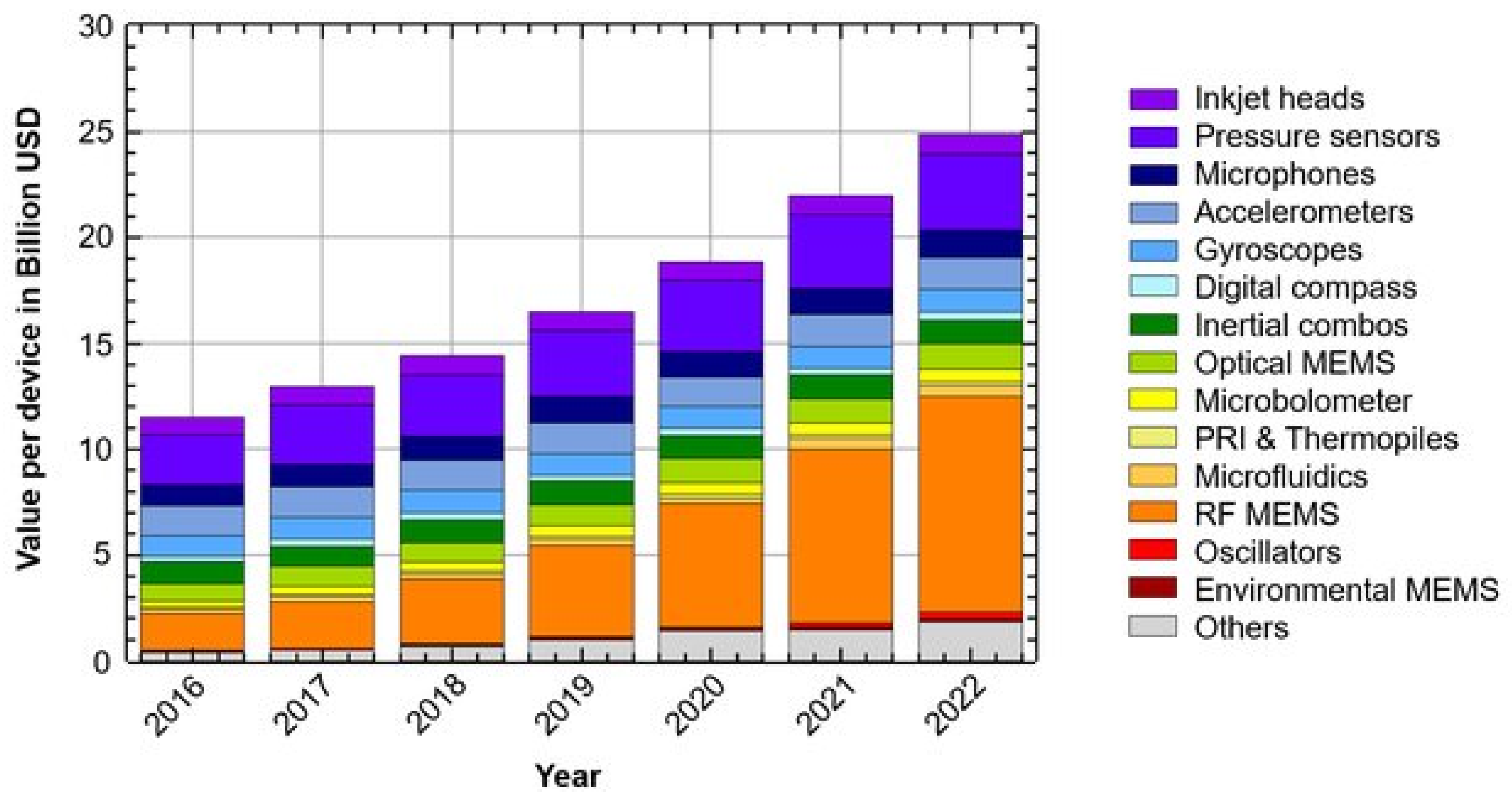
1. Introduction
2. MEMS Fabrication Strategies
2.1. Materials
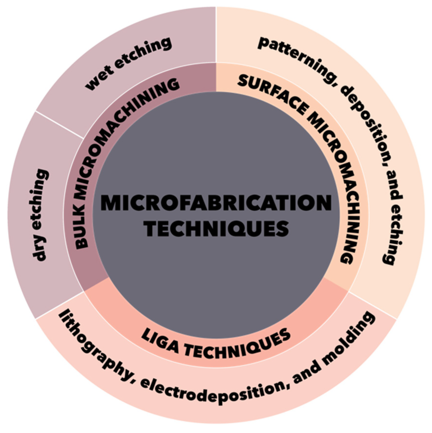
2.2. Microfabrication Techniques
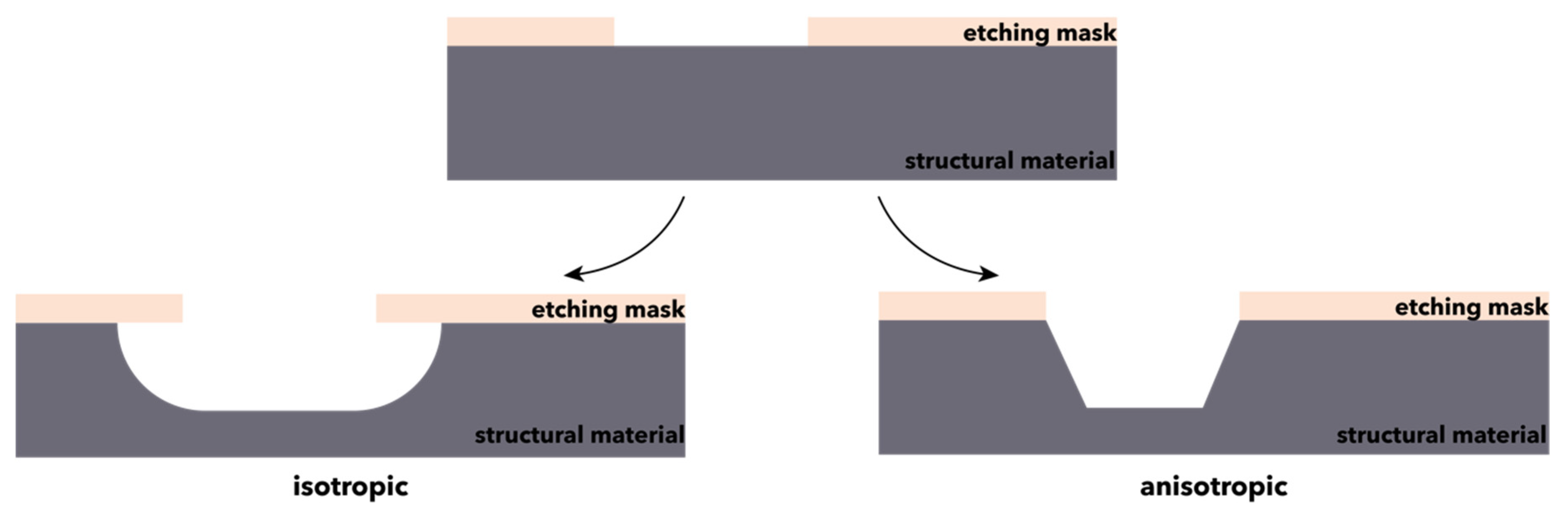
2.2.1. Bulk Micromachining
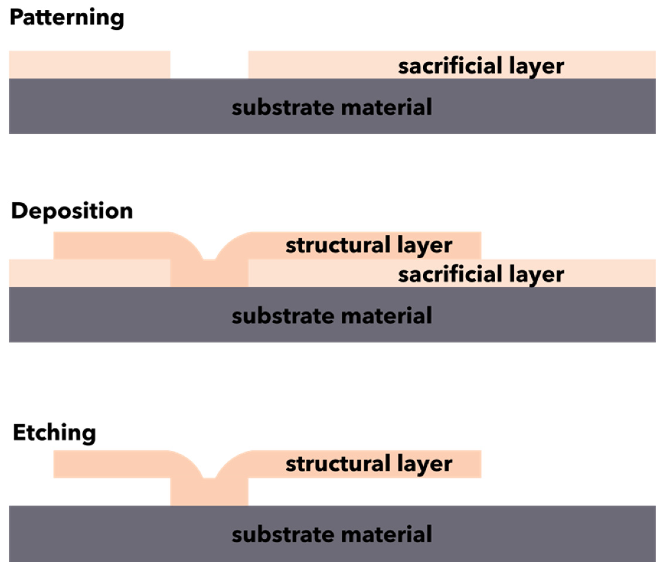
2.2.2. Surface Micromachining
2.2.3. LIGA Techniques
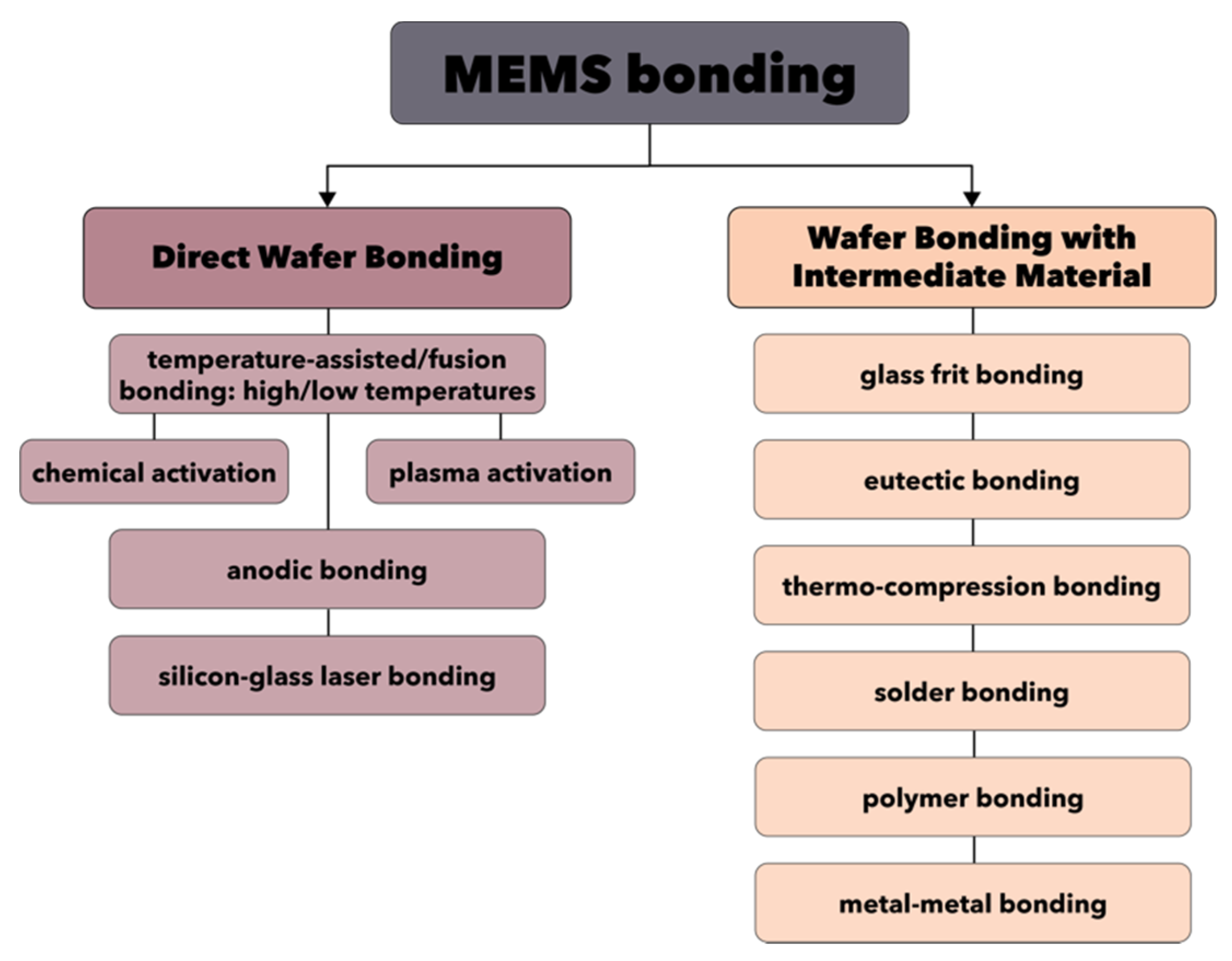
2.2.4. MEMS Bonding Methods
3. MEMS-Based Microfluidic Devices
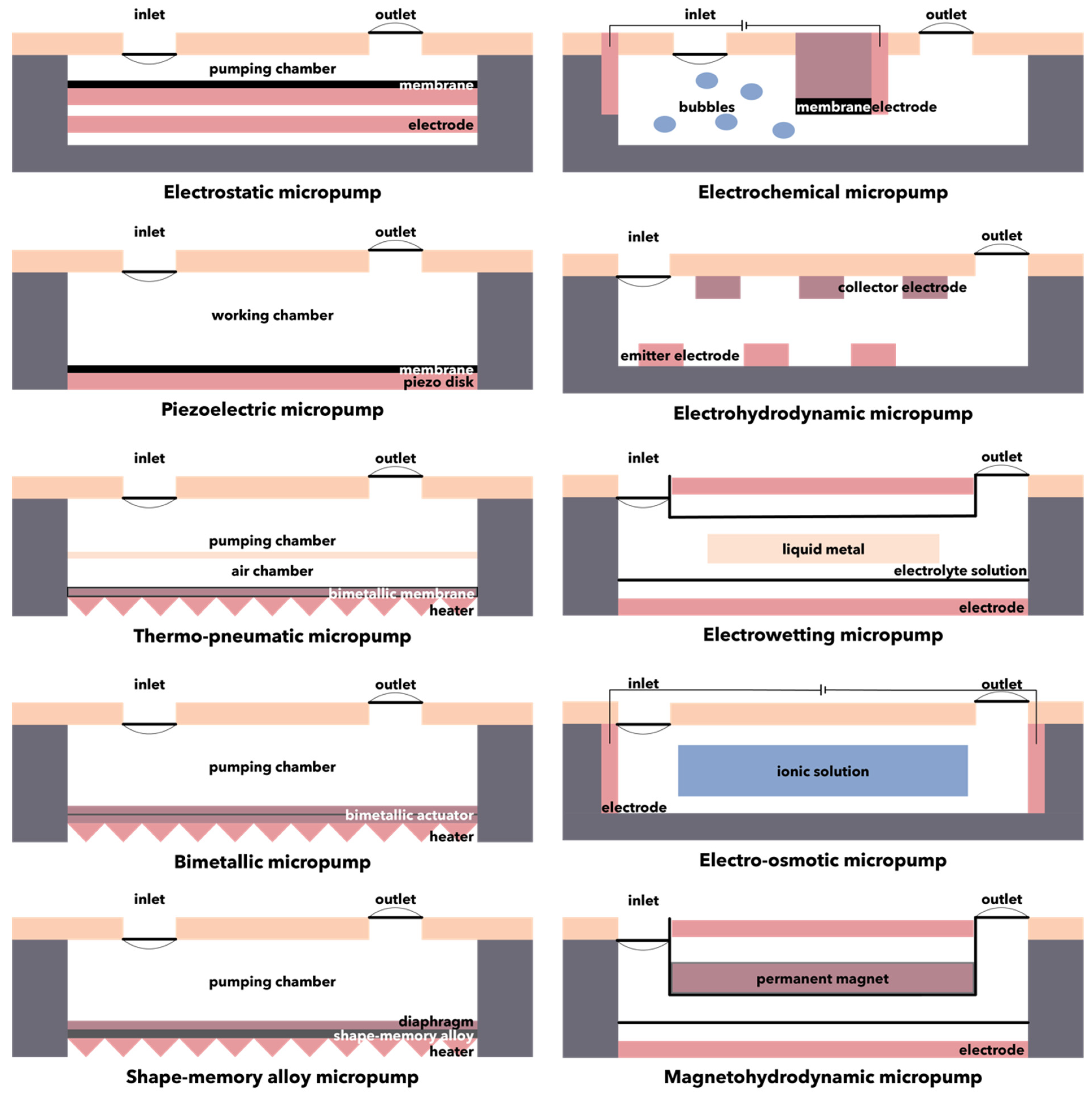
3.1. Micropumps
3.1.1. Electrostatic Micropumps
3.1.2. Piezoelectric Micropumps
3.1.3. Thermo-Pneumatic Micropumps
3.1.4. Bimetallic Micropumps
3.1.5. Shape-Memory Alloy Micropumps
3.1.6. Ionic Conductive Polymeric Films Micropumps
3.1.7. Electrochemical Micropumps
3.1.8. Electrohydrodynamic Micropumps
3.1.9. Electrowetting Micropumps
3.1.10. Electro-Osmotic Micropumps
3.1.11. Magnetohydrodynamic Micropumps
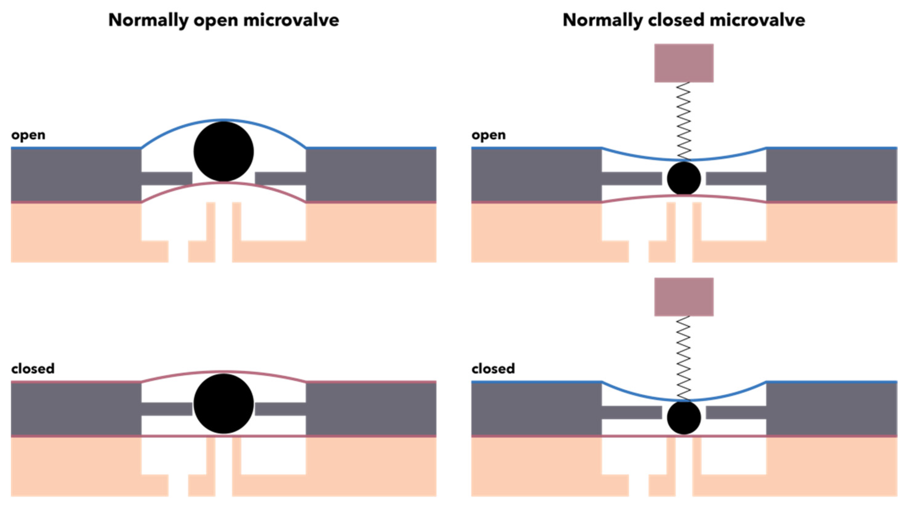
3.2. Microvalves
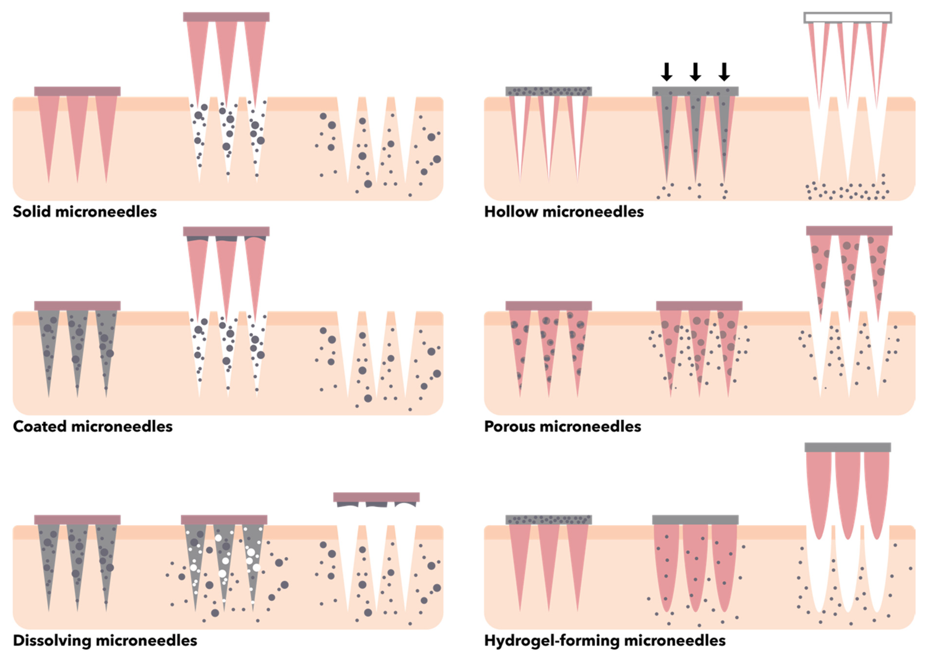
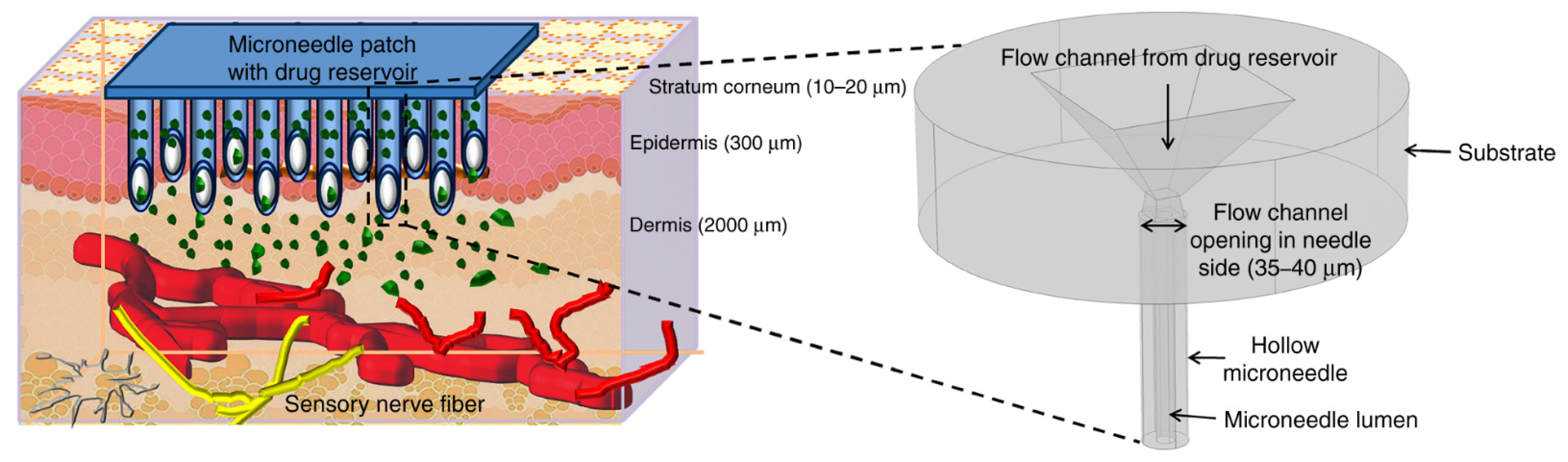
3.3. Microneedles
3.4. Micromixers
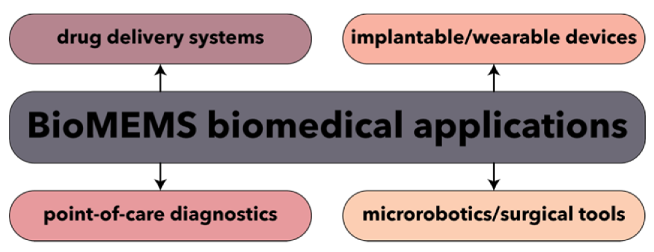
4. Biomedical Applications of MEMS Devices
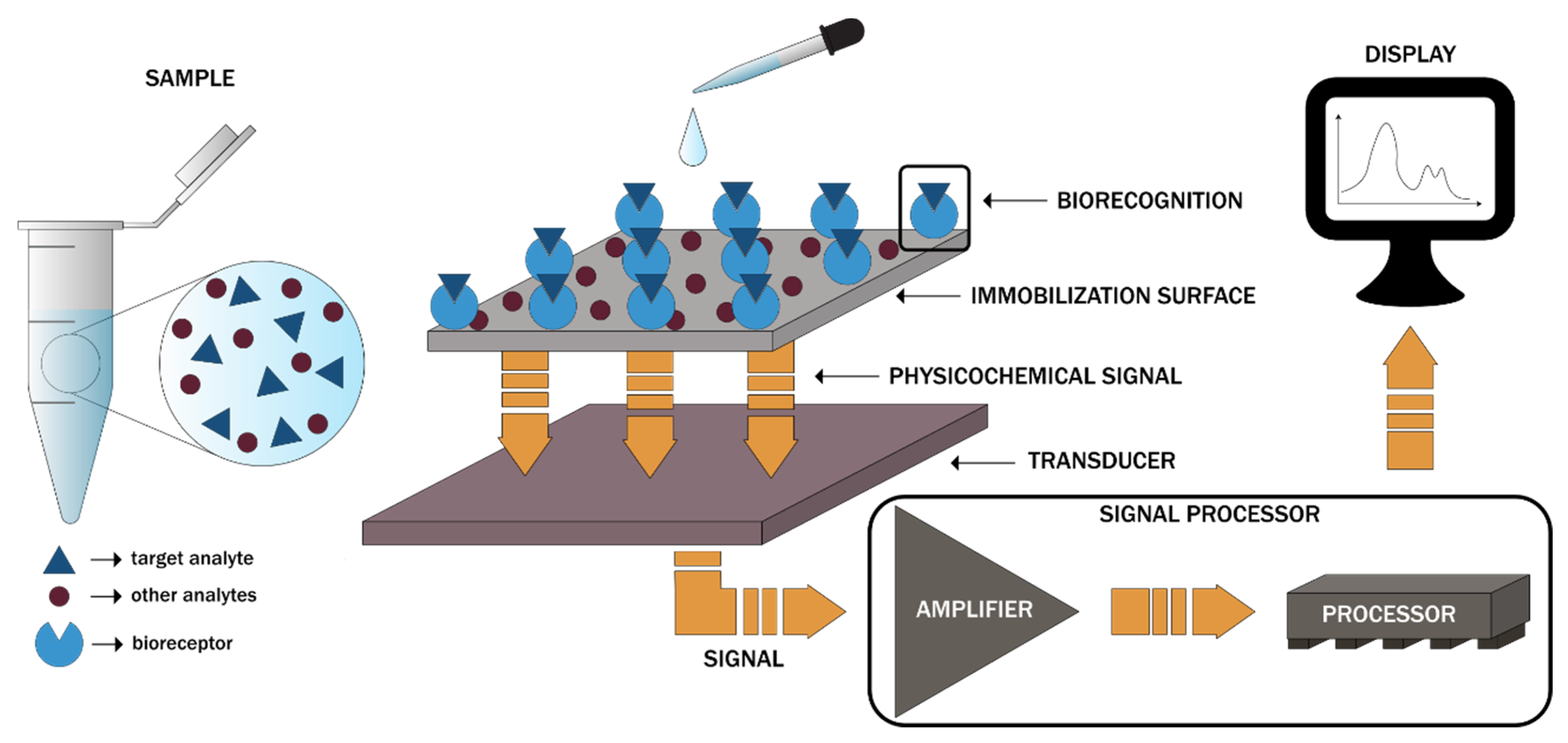
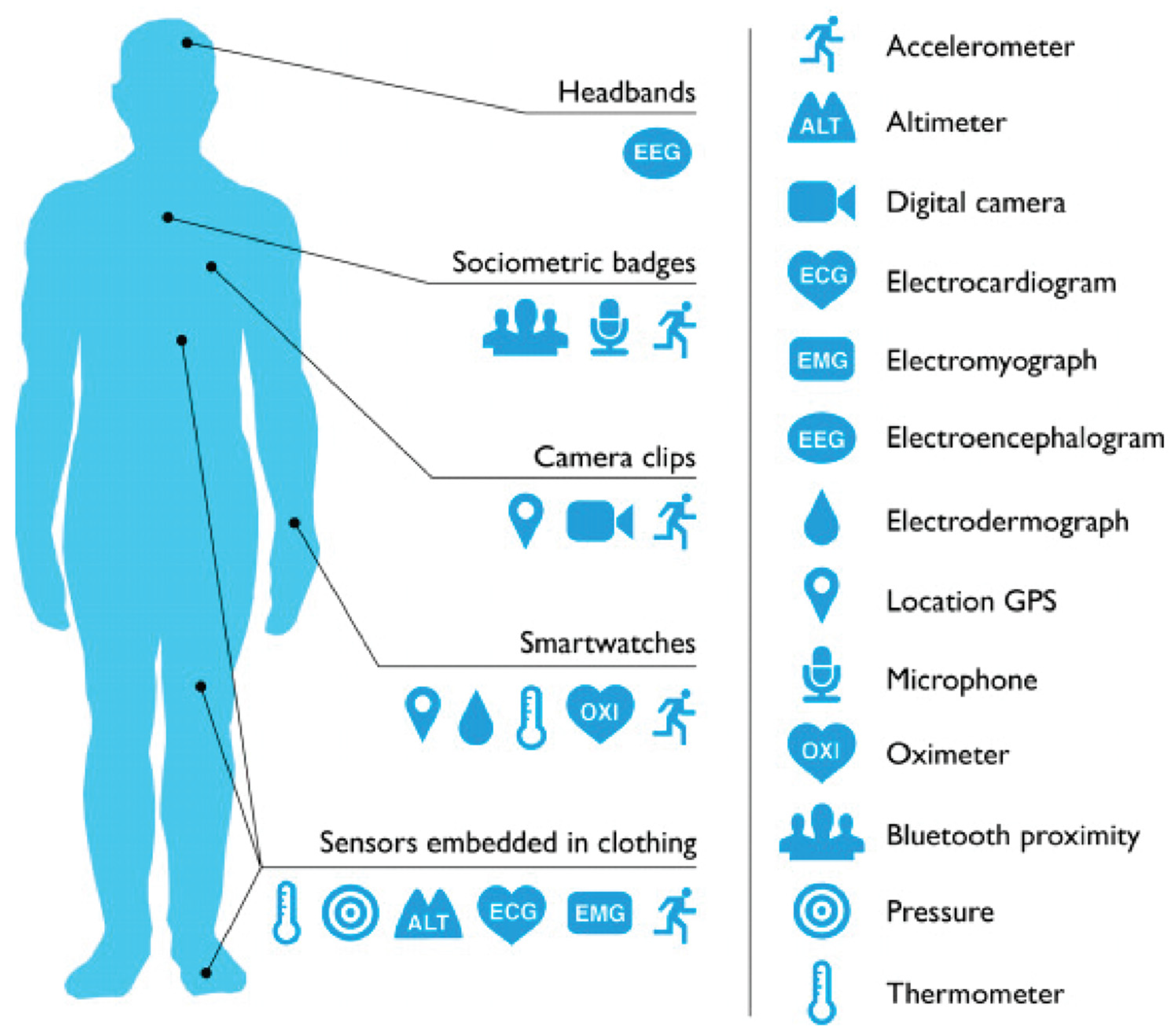
4.1. Disease Diagnostics
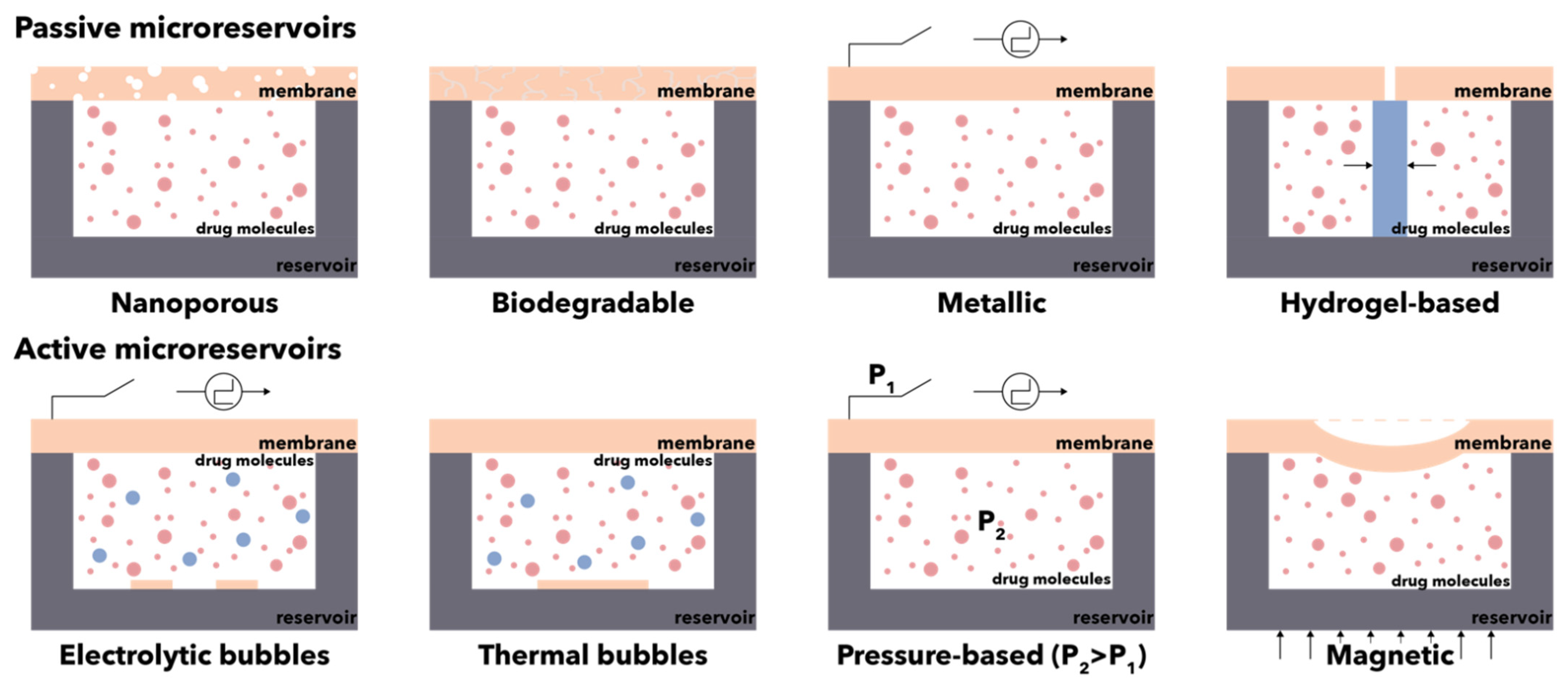
4.2. Drug Delivery
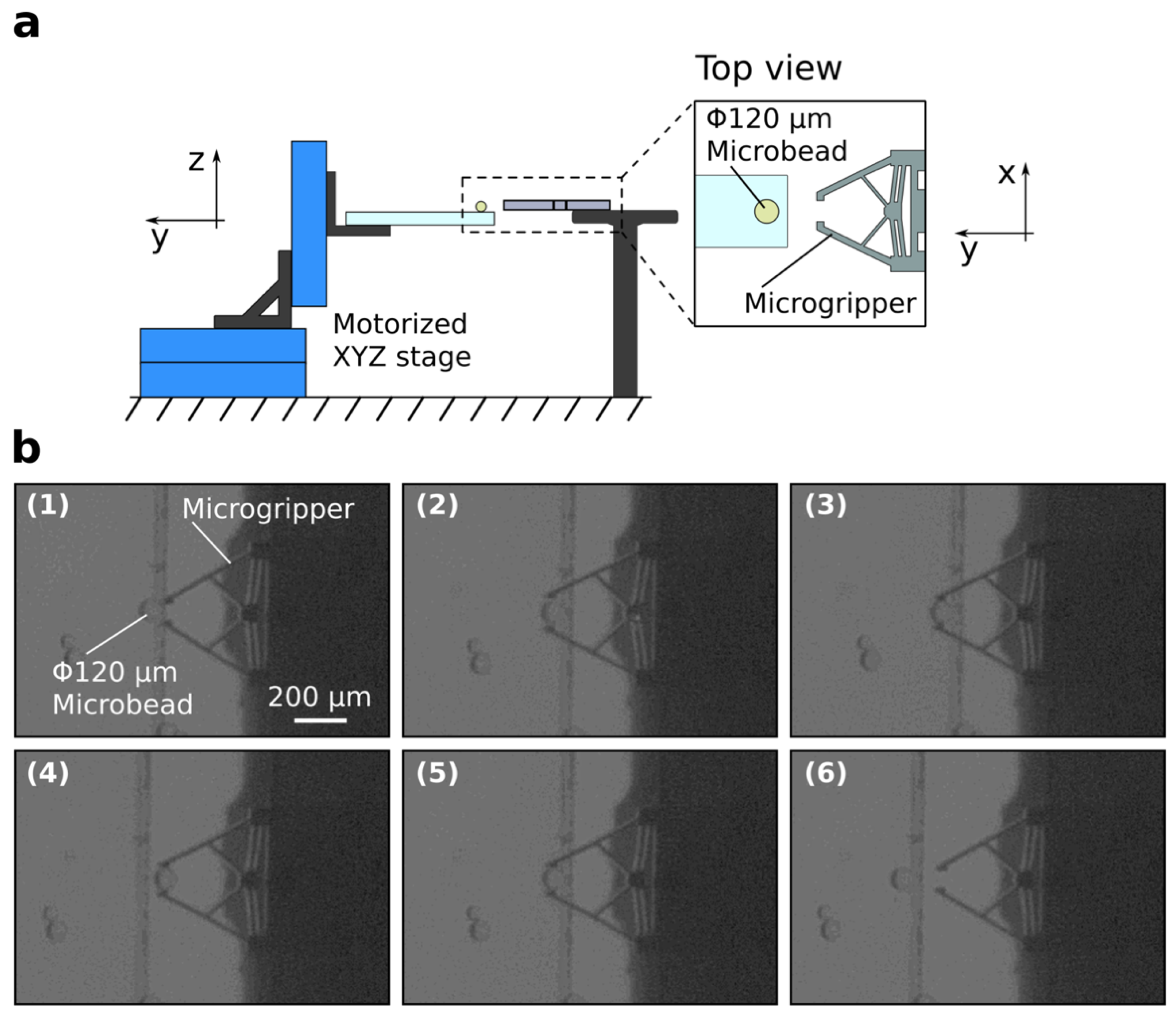
4.3. Microrobotics and Surgical Tools
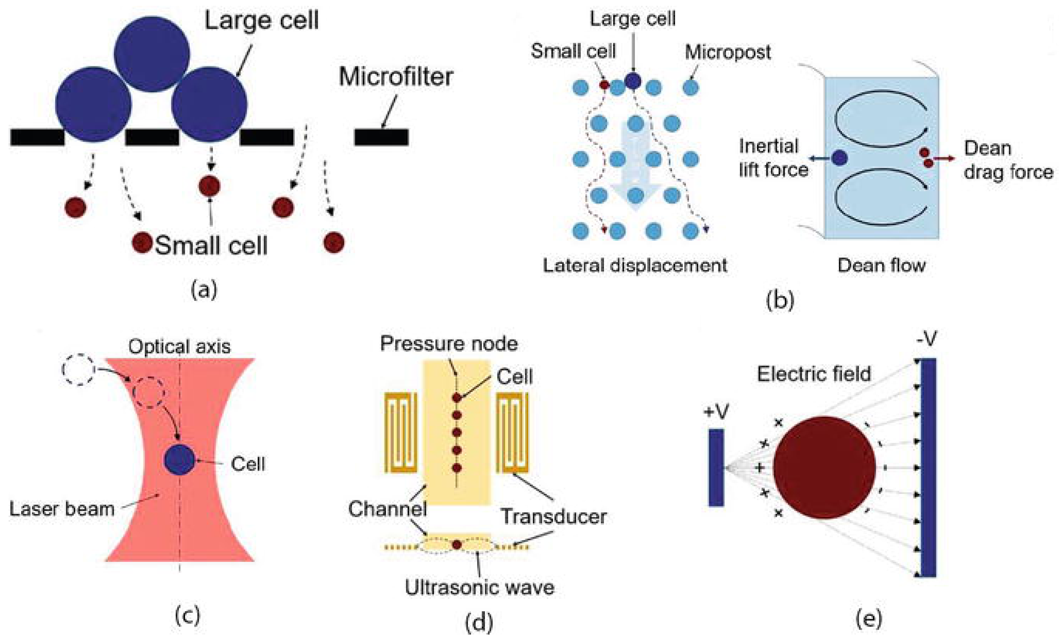
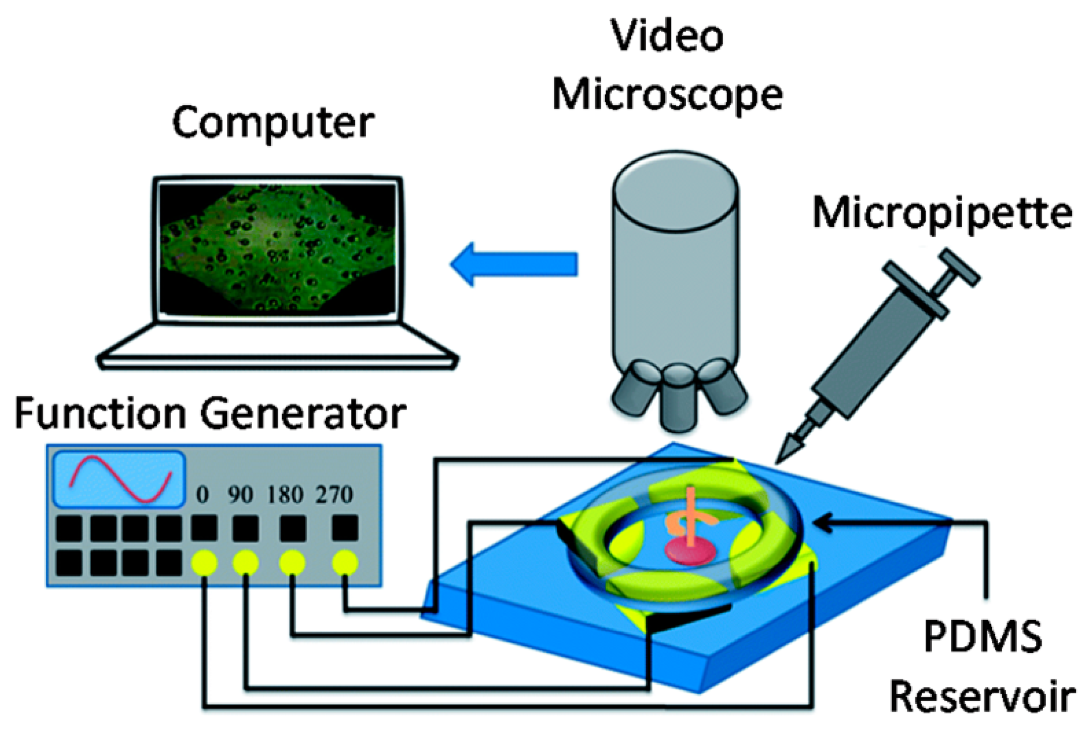
4.4. Cell and Gene Manipulation and Characterization
5. Challenges and Future Directions
6. Conclusions
Author Contributions
Funding
Conflicts of Interest
References
- Putrino, G.; Keating, A.; Martyniuk, M.; Faraone, L.; Dell, J. Chemical and biological sensors based on microelectromechanical systems. In Nanomaterials: Science and Applications; Pan Stanford Publishing Pte Ltd.: Singapore, 2016; pp. 107–145. [Google Scholar]
- Shanbhag, P.P.; Patil, N.S. BioMicroelectromechanical systems: A novel approach for drug targeting in chronic diseases. New Horiz. Transl. Med. 2017, 3, 265–271. [Google Scholar] [CrossRef]
- Yunjia, L. Microelectromechanical systems (MEMS). In Material-Integrated Intelligent Systems: Technology and Applications; John Wiley & Sons: New York, NY, USA, 2016; pp. 83–105. [Google Scholar]
- Rafiee, P.; Khatibi, G.; Zehetbauer, M. A review of the most important failure, reliability and nonlinearity aspects in the development of microelectromechanical systems (MEMS). Microelectron. Int. 2017, 34, 9–21. [Google Scholar] [CrossRef]
- Kavallaris, N.I.; Suzuki, T. Micro-Electro-Mechanical-Systems (MEMS). In Non-Local Partial Differential Equations for Engineering and Biology: Mathematical Modeling and Analysis; Springer: Tokyo, Japan, 2018; Volume 31, pp. 3–63. [Google Scholar]
- Herrera-May, A.L.; Soler-Balcazar, J.C.; Vázquez-Leal, H.; Martínez-Castillo, J.; Vigueras-Zuñiga, M.O.; Aguilera-Cortés, L.A. Recent Advances of MEMS Resonators for Lorentz Force Based Magnetic Field Sensors: Design, Applications and Challenges. Sensors 2016, 16, 1359. [Google Scholar] [CrossRef] [PubMed]
- Puers, R.; Baldi, L.; Van de Voorde, M. Conclusions. In Nanoelectronics: Materials, Devices, Applications; John Wiley & Sons: New York, NY, USA, 2017; Volume 1, pp. 613–616. [Google Scholar]
- Jivani, R.R.; Lakhtaria, G.J.; Patadiya, D.D.; Patel, L.D.; Jivani, N.P.; Jhala, B.P. RETRACTED: Biomedical microelectromechanical systems (BioMEMS): Revolution in drug delivery and analytical techniques. Saudi Pharm. J. 2016, 24, 1–20. [Google Scholar] [CrossRef]
- Bergveld, P. The Challenge of Developing µTAS. In Micro Total Analysis Systems; Springer: Dordrecht, The Netherlands, 1955; pp. 1–4. [Google Scholar]
- Zhang, B.; Li, Q.; Yan, S.; Zhang, Y.; Yang, G.; Wang, C.; Cui, H. The principle and elimination of shadow image in the scanning image of the lidar based on MEMS mirror. Infrared Phys. Technol. 2021, 116, 103761. [Google Scholar] [CrossRef]
- Han, X.; Xu, M.; Li, G.; Yan, H.; Feng, Y.; Li, D. Design and experiment of a touch mode MEMS capacitance vacuum gauge with square diaphragm. Sens. Actuators A Phys. 2020, 313, 112154. [Google Scholar] [CrossRef]
- Li, G.; Han, X.; Sun, W.; Cheng, Y.; Li, D. A touch mode MEMS capacitance diaphragm gauge. Meas. Sens. 2021, 18, 100171. [Google Scholar] [CrossRef]
- Zaghloul, U.; Bhushan, B.; Papaioannou, G.; Coccetti, F.; Pons, P.; Plana, R. Nanotribology-based novel characterization techniques for the dielectric charging failure mechanism in electrostatically actuated NEMS/MEMS devices using force–distance curve measurements. J. Colloid Interface Sci. 2012, 365, 236–253. [Google Scholar] [CrossRef]
- Zhang, W.; Ji, S.; Liang, X.; Zhang, G.; Wang, R.; Chen, P.; Zhu, S.; Liu, Y.; Jing, B.; Zhang, Y.; et al. Research on the Influence of Hydrostatic Pressure on the Sensitivity of Bionic Cilia MEMS Vector Hydrophone. Measurement 2021, 20, 110606. [Google Scholar] [CrossRef]
- Casillas, A.; Modera, M.; Pritoni, M. Using non-invasive MEMS pressure sensors for measuring building envelope air leakage. Energy Build. 2021, 233, 110653. [Google Scholar] [CrossRef]
- Grzebyk, T.; Turczyk, K.; Szyszka, P.; Górecka-Drzazga, A.; Dziuban, J. Pressure control system for vacuum MEMS. Vacuum 2020, 178, 109452. [Google Scholar] [CrossRef]
- Kishore, K.; Kumar, S.S.; Mukhiya, R.; Akbar, S.A. High-resolution current mode interface for MEMS piezoresistive pressure sensor. AEU-Int. J. Electron. Commun. 2021, 134, 153707. [Google Scholar] [CrossRef]
- Xu, M.; Feng, Y.; Han, X.; Ke, X.; Li, G.; Zeng, Y.; Yan, H.; Li, D. Design and fabrication of an absolute pressure MEMS capacitance vacuum sensor based on silicon bonding technology. Vacuum 2021, 186, 110065. [Google Scholar] [CrossRef]
- Cheng, C.-C.; Fang, L.-H.; Duan, H.; Chen, C.-C.; Chung, T.-K. A MEMS room-temperature resettable thermomagnetic-track-guided magnetic-bead manipulation integrated with magnetoresistive sensing for bead-motion monitoring. Sens. Actuators A Phys. 2021, 332, 113087. [Google Scholar] [CrossRef]
- Paes, V.F.; Mueller, B.A.; Costa, P.B.; Ferreira, R.A.M.; Porto, M.P. Calibration uncertainty of MEMS thermopile imagers for quantitative temperature measurement. Infrared Phys. Technol. 2022, 120, 103978. [Google Scholar] [CrossRef]
- Krisper, R.; Lammer, J.; Pivak, Y.; Fisslthaler, E.; Grogger, W. The Performance of EDXS at Elevated Sample Temperatures Using a MEMS-Based In Situ TEM Heating System. Ultramicroscopy 2021, 31, 113461. [Google Scholar] [CrossRef]
- Chung, V.P.J.; Yip, M.-C.; Fang, W. Resorcinol–formaldehyde aerogels for CMOS-MEMS capacitive humidity sensor. Sens. Actuators B Chem. 2015, 214, 181–188. [Google Scholar] [CrossRef]
- Jan, M.T.; Ahmad, F.; Hamid, N.H.B.; Khir, M.H.B.M.; Shoaib, M.; Ashraf, K. Experimental investigation of temperature and relative humidity effects on resonance frequency and quality factor of CMOS-MEMS paddle resonator. Microelectron. Reliab. 2016, 63, 82–89. [Google Scholar] [CrossRef]
- Hassan, A.S.; Juliet, V.; Raj, C.J.A. MEMS Based Humidity Sensor with Integration of Temperature Sensor. Mater. Today Proc. 2018, 5, 10728–10737. [Google Scholar] [CrossRef]
- Xu, J.; Bertke, M.; Li, X.; Mu, H.; Zhou, H.; Yu, F.; Hamdana, G.; Schmidt, A.; Bremers, H.; Peiner, E. Fabrication of ZnO nanorods and Chitosan@ZnO nanorods on MEMS piezoresistive self-actuating silicon microcantilever for humidity sensing. Sens. Actuators B Chem. 2018, 273, 276–287. [Google Scholar] [CrossRef]
- Faraci, D.; Ghisi, A.; Adorno, S.; Corigliano, A. Top-down, multi-scale numerical simulation of MEMS microphones under guided free fall tests. Microelectron. Reliab. 2021, 121, 114129. [Google Scholar] [CrossRef]
- Fawzy, A.; Magdy, A.; Hossam, A. A piezoelectric MEMS microphone optimizer platform. Alex. Eng. J. 2022, 61, 3175–3186. [Google Scholar] [CrossRef]
- Novak, A.; Honzík, P. Measurement of nonlinear distortion of MEMS microphones. Appl. Acoust. 2021, 175, 107802. [Google Scholar] [CrossRef]
- Wenzel, T.; Rettig, R. Design of MEMS microphone protective membranes for continuous outdoor applications. Appl. Acoust. 2021, 183, 108304. [Google Scholar] [CrossRef]
- Din, H.; Iqbal, F.; Lee, B. Mode ordering of single-drive multi-axis MEMS gyroscope for reduced cross-axis sensitivity. Sens. Actuators A Phys. 2021, 332, 113145. [Google Scholar] [CrossRef]
- Jia, J.; Ding, X.; Qin, Z.; Ruan, Z.; Li, W.; Liu, X.; Li, H. Overview and analysis of MEMS Coriolis vibratory ring gyroscope. Measurement 2021, 182, 109704. [Google Scholar] [CrossRef]
- Luo, S.; Yang, G.; Li, J.; Ouakad, H.M. Dynamic analysis, circuit realization and accelerated adaptive backstepping control of the FO MEMS gyroscope. Chaos Solitons Fractals 2022, 155, 111735. [Google Scholar] [CrossRef]
- Zirkohi, M.M. Adaptive backstepping control design for MEMS gyroscope based on function approximation techniques with input saturation and output constraints. Comput. Electr. Eng. 2022, 97, 107547. [Google Scholar] [CrossRef]
- Chen, M.; Zhu, R.; Lin, Y.; Zhao, Z.; Che, L. Analysis and compensation for nonlinearity of sandwich MEMS capacitive accelerometer induced by fabrication process error. Microelectron. Eng. 2022, 252, 111672. [Google Scholar] [CrossRef]
- Morozov, N.F.; Indeitsev, D.A.; Igumnova, V.S.; Lukin, A.V.; Popov, I.A.; Shtukin, L.V. Nonlinear dynamics of mode-localized MEMS accelerometer with two electrostatically coupled microbeam sensing elements. Int. J. Non-Linear Mech. 2022, 138, 103852. [Google Scholar] [CrossRef]
- Prato, A.; Mazzoleni, F.; D’Emilia, G.; Gaspari, A.; Natale, E.; Schiavi, A. Metrological traceability of a digital 3-axis MEMS accelerometers sensor network. Measurement 2021, 184, 109925. [Google Scholar] [CrossRef]
- Tariq, S.; Bakhtawar, B.; Zayed, T. Data-driven application of MEMS-based accelerometers for leak detection in water distribution networks. Sci. Total Environ. 2022, 809, 151110. [Google Scholar] [CrossRef] [PubMed]
- Dellea, S.; Laghi, G.; Langfelder, G.; Longoni, A.; Minotti, P.; Tocchio, A.; Zerbini, S. Off-resonance Operation of In-plane Torsional MEMS Magnetometers. Procedia Eng. 2014, 87, 819–822. [Google Scholar] [CrossRef]
- Laghi, G.; Dellea, S.; Longoni, A.; Minotti, P.; Tocchio, A.; Zerbini, S.; Langfelder, G. Torsional MEMS magnetometer operated off-resonance for in-plane magnetic field detection. Sens. Actuators A Phys. 2015, 229, 218–226. [Google Scholar] [CrossRef]
- Liu, S.; Liang, H.; Xiong, B. An out-of-plane electromagnetic induction based resonant MEMS magnetometer. Sens. Actuators A Phys. 2019, 285, 248–257. [Google Scholar] [CrossRef]
- Qu, H. CMOS MEMS Fabrication Technologies and Devices. Micromachines 2016, 7, 14. [Google Scholar] [CrossRef]
- Langfelder, G.; Tocchio, A. 15-Microelectromechanical systems integrating motion and displacement sensors. In Smart Sensors and MEMs, 2nd ed.; Nihtianov, S., Luque, A., Eds.; Woodhead Publishing: Cambridge, UK, 2018; pp. 395–428. [Google Scholar]
- Stefan, W.; Niklaus, F.; Mokwa, W.; Lemme, M.C. 2D Materials for Piezoresistive Strain Gauges and Membrane Based Nanoelectromechanical Systems. Ph.D. Thesis, RWTH Aachen University, Aachen, Germany, 2018. [Google Scholar]
- Lyshevski, S.E. MEMS and NEMS: Systems, Devices, and Structures; CRC Press: New York, NY, USA, 2018. [Google Scholar]
- Anjanappa, M.; Datta, K.; Song, T. Introduction to sensors and actuators. In Mechatronic Systems, Sensors, and Actuators: Fundamentals and Modeling; CRC Press: New York, NY, USA, 2017; pp. 11–16. [Google Scholar]
- Giang, D.T.H.; Duc, N.H.; Agnus, G.; Maroutian, T.; Lecoeur, P. Fabrication and characterization of PZT string based MEMS devices. J. Sci. Adv. Mater. Devices 2016, 1, 214–219. [Google Scholar] [CrossRef][Green Version]
- Goldfarb, M.; Strauss, A.M.; Barth, E.J. An introduction to micro- and nanotechnology. In Mechatronic Systems, Sensors, and Actuators: Fundamentals and Modeling; CRC Press: New York, NY, USA, 2017. [Google Scholar]
- Khoshnoud, F.; de Silva, C.W.; Esat, I. Bio-MEMS Sensors and Actuators; Crc Press-Taylor & Francis Group: Boca Raton, FL, USA, 2016; pp. 221–252. [Google Scholar]
- Lee, C.; Kim, J.Y.; Kim, C. Recent Progress on Photoacoustic Imaging Enhanced with Microelectromechanical Systems (MEMS) Technologies. Micromachines 2018, 9, 584. [Google Scholar] [CrossRef]
- Tao, K.; Wu, J.; Kottapalli, A.G.P.; Lye, S.W.; Miao, J. MEMS/NEMS-Enabled Vibrational Energy Harvesting for Self-Powered and Wearable Electronics. In Outlook and Challenges of Nano Devices, Sensors, and MEMS; Springer: Cham, Switzerland, 2017; pp. 271–297. [Google Scholar]
- Yao, W.; Peddi, R. Customizable silicone materials for MEMS and semiconductor packages. In Proceedings of the 2016 IEEE 37th International Electronics Manufacturing Technology (IEMT) & 18th Electronics Materials and Packaging (EMAP) Conference, Georgetown, Malaysia, 20–22 September 2016; pp. 1–6. [Google Scholar]
- Shoaib, M.; Hamid, N.H.; Malik, A.F.; Ali, N.B.Z.; Jan, M.T. A Review on Key Issues and Challenges in Devices Level MEMS Testing. J. Sens. 2016, 2016, 1639805. [Google Scholar] [CrossRef]
- Lee, Y.C.; Kong, M.; Zhang, Y. Microelectromechanical Systems and Packaging. In Materials for Advanced Packaging; Lu, D., Wong, C.P., Eds.; Springer International Publishing: Cham, Switzerland, 2017; pp. 697–731. [Google Scholar]
- Keçili, R.; Büyüktiryaki, S.; Hussain, C.M. 8—Micro total analysis systems with nanomaterials. In Handbook of Nanomaterials in Analytical Chemistry; Hussain, C.M., Ed.; Elsevier: Amsterdam, The Netherlands, 2020; pp. 185–198. [Google Scholar]
- Araya-Farias, M.; Dziomba, S.; Tran, N.T. Chapter 3—Microfluidic strategies for extraction and preconcentration of proteins and peptides. In Handbook on Miniaturization in Analytical Chemistry; Hussain, C.M., Ed.; Elsevier: Amsterdam, The Netherlands, 2020; pp. 35–75. [Google Scholar]
- Gaudin, V. Chapter 11—Receptor-based electrochemical biosensors for the detection of contaminants in food products. In Electrochemical Biosensors; Ensafi, A.A., Ed.; Elsevier: Amsterdam, The Netherlands, 2019; pp. 307–365. [Google Scholar] [CrossRef]
- Liang, Z.; Guo, J.; Fan, D. 1—Manipulation, assembling, and actuation of nanomotors by electric tweezers. In Robotic Systems and Autonomous Platforms; Walsh, S.M., Strano, M.S., Eds.; Woodhead Publishing: Cambridge, UK, 2019; pp. 3–28. [Google Scholar]
- Tung, J.; Gower, S.; Ooteghem, K.V.; Nouredanesh, M.; Gage, W.H. Chapter 5—Point of care technologies. In Digital Health; Godfrey, A., Stuart, S., Eds.; Academic Press: Cambridge, MA, USA, 2021; pp. 73–84. [Google Scholar]
- Bretschneider, F.; de Weille, J. Chapter 8—Recording of Electrophysiological Signals. In Introduction to Electrophysiological Methods and Instrumentation, 2nd ed.; Bretschneider, F., de Weille, J., Eds.; London Academic Press: London, UK, 2019; pp. 201–240. [Google Scholar]
- Huang, L.; Zhao, P.; Liang, F.; Wang, W. Chapter 5—Single-cell 3D electro-rotation. In Methods in Cell Biology; Fletcher, D.A., Doh, J., Piel, M., Eds.; Academic Press: Cambridge, MA, USA, 2018; Volume 148, pp. 97–116. [Google Scholar]
- Martinez-Rivas, A.; González-Quijano, G.K.; Proa-Coronado, S.; Séverac, C.; Dague, E. Methods of Micropatterning and Manipulation of Cells for Biomedical Applications. Micromachines 2017, 8, 347. [Google Scholar] [CrossRef]
- Pan, P.; Wang, W.; Ru, C.; Sun, Y.; Liu, X. MEMS-based platforms for mechanical manipulation and characterization of cells. J. Micromech. Microeng. 2017, 27, 123003. [Google Scholar] [CrossRef]
- Chorsi, M.T.; Curry, E.J.; Chorsi, H.T.; Das, R.; Baroody, J.; Purohit, P.K.; Ilies, H.; Nguyen, T.D. Piezoelectric Biomaterials for Sensors and Actuators. Adv. Mater. 2019, 31, e1802084. [Google Scholar] [CrossRef] [PubMed]
- Daoudi, K.; Gaidi, M.; Columbus, S. Biointerface Research in Applied Chemistry. Ultrasound 2017, 69, 70. [Google Scholar]
- Teh, K.S. Additive direct-write microfabrication for MEMS: A review. Front. Mech. Eng. 2017, 12, 490–509. [Google Scholar] [CrossRef]
- Qin, D.; Xia, Y.; Rogers, J.A.; Jackman, R.J.; Zhao, X.-M.; Whitesides, G.M. Microfabrication, microstructures and microsystems. Microsyst. Technol. Chem. Life Sci. 1998, 194, 1–20. [Google Scholar]
- Zorman, C.A. Materials Aspects of Micro- and Nanoelectromechanical Systems. In Springer Handbook of Nanotechnology; Bhushan, B., Ed.; Springer: Berlin/Heidelberg, Germany, 2017; pp. 203–224. [Google Scholar]
- Kim, B.J.; Meng, E. Review of polymer MEMS micromachining. J. Micromech. Microeng. 2015, 26, 013001. [Google Scholar] [CrossRef]
- Buitrago, L.; Ortiz, C.; Barrientos, K.; Jaramillo, M. Development of a high frequency piezoelectric immunosensor for the detection and quantification of BSA. Biointerface Res. Appl. Chem. 2020, 10, 5400–5405. [Google Scholar]
- Prabakar, A.; Killivalavan, G.; Sivakumar, D.; Chandra Babu Naidu, K.; Sathyaseelan, B.; Senthilnathan, K.; Baskaran, I.; Elayaperumal, M.; Rao, B.; Sarma, S.; et al. Structural, morphological, and magnetic properties of copper zinc cobalt ferrites systems nanocomposites. Biointerface Res. Appl. Chem. 2020, 10, 6015–6019. [Google Scholar] [CrossRef]
- Badry, R.; Ibrahim, A.; Gamal, F.; Shehata, D.; Ezzat, H.; Elhaes, H.; Ibrahim, M. Electronic Properties of Polyvinyl Alcohol/TiO2/SiO2 Nanocomposites. Biointerface Res. Appl. Chem. 2020, 10, 6427–6435. [Google Scholar]
- Amiri, I.S.; Ariannejad, M.M.; Vigneswaran, D.; Lim, C.S.; Yupapin, P. Performances and procedures modules in micro electro mechanical system packaging technologies. Results Phys. 2018, 11, 306–314. [Google Scholar] [CrossRef]
- Horst, J.; de Andreade, P.; Duvoisin, C.A.; Vieira, R. Fabrication of conductive filaments for 3D-printing: Polymer nanocomposites. Biointerface Res. Appl. Chem. 2020, 10, 6577–6586. [Google Scholar]
- Kenawy, S.; Khalil, A. Advanced ceramics and relevant polymers for environmental and biomedical applications. Biointerface Res. Appl. Chem 2020, 10, 5747–5754. [Google Scholar]
- Funano, S.-i.; Ota, N.; Tanaka, Y. A simple and reversible glass–glass bonding method to construct a microfluidic device and its application for cell recovery. Lab Chip 2021, 21, 2244–2254. [Google Scholar] [CrossRef] [PubMed]
- Wang, T.; Chen, J.; Zhou, T.; Song, L. Fabricating Microstructures on Glass for Microfluidic Chips by Glass Molding Process. Micromachines 2018, 9, 269. [Google Scholar] [CrossRef]
- Wlodarczyk, K.L.; Hand, D.P.; Maroto-Valer, M.M. Maskless, rapid manufacturing of glass microfluidic devices using a picosecond pulsed laser. Sci. Rep. 2019, 9, 20215. [Google Scholar] [CrossRef] [PubMed]
- Korobova, N. Piezoelectric MEMS Technologies. In Advanced Piezoelectric Materials: Science and Technology, 2nd ed.; Uchino, K., Ed.; Woodhead Publ Ltd.: Cambridge, MA, USA, 2017; pp. 533–574. [Google Scholar]
- Lyshevski, S.E. Rotational and translational microelectromechanical systems: MEMS synthesis, microfabrication, analysis, and optimization. In Mechatronic Systems, Sensors, and Actuators: Fundamentals and Modeling; CRC Press: New York, NY, USA, 2017. [Google Scholar]
- Coutu, R.A., Jr. Additive manufacturing at the micron scale. In Additive Manufacturing Handbook: Product Development for the Defense Industry; CRC Press: Boca Raton, FL, USA, 2017; pp. 381–388. [Google Scholar]
- Dragoman, M.; Dragoman, D. Instruments/Devices. Microelectromechanical Systems. In Reference Module in Materials Science and Materials Engineering; Elsevier: Amsterdam, The Netherlands, 2016. [Google Scholar] [CrossRef]
- Hildreth, O.; Wong, C.P. Nano-metal-Assisted Chemical Etching for Fabricating Semiconductor and Optoelectronic Devices. In Materials for Advanced Packaging; Lu, D., Wong, C.P., Eds.; Springer International Publishing: Cham, Switzerland, 2017; pp. 879–922. [Google Scholar] [CrossRef]
- Dziuban, J.A. Bonding in Microsystem Technology; Springer Science & Business Media: Berlin/Heidelberg, Germany, 2007; Volume 24. [Google Scholar]
- Bhushan, B. Nanotribology and Nanomechanics of MEMS/NEMS and BioMEMS/BioNEMS Materials and Devices. In Nanotribology and Nanomechanics: An Introduction; Bhushan, B., Ed.; Springer International Publishing: Cham, Switzerland, 2017; pp. 797–907. [Google Scholar]
- Bhushan, B. Nanomechanical Properties of Nanostructures and Scale Effects. In Nanotribology and Nanomechanics: An Introduction; Bhushan, B., Ed.; Springer International Publishing: Cham, Switzerland, 2017; pp. 253–299. [Google Scholar]
- Malinovskaya, Y.; Melnikov, P.; Baklaushev, V.; Gabashvili, A.; Osipova, N.; Mantrov, S.; Ermolenko, Y.; Maksimenko, O.; Gorshkova, M.; Balabanyan, V.; et al. Delivery of doxorubicin-loaded PLGA nanoparticles into U87 human glioblastoma cells. Int. J. Pharm. 2017, 524, 77–90. [Google Scholar] [CrossRef]
- Je, C.H.; Lee, S.Q.; Yang, W.S. High Sensitivity Surface Micromachined Absolute Pressure Sensor. Procedia Eng. 2016, 168, 725–728. [Google Scholar] [CrossRef]
- Cheng, H.-C. Wet Etching. In Handbook of Visual Display Technology; Chen, J., Cranton, W., Fihn, M., Eds.; Springer International Publishing: Cham, Switzerland, 2016; pp. 1331–1341. [Google Scholar]
- Sarangan, A. 5-Nanofabrication. In Fundamentals and Applications of Nanophotonics; Haus, J.W., Ed.; Woodhead Publishing: Cambridge, UK, 2016; pp. 149–184. [Google Scholar] [CrossRef]
- Dziuban, J.A. Deep, Three-Dimensional Silicon Micromachining. Bond. Microsyst. Technol. 2006, 24, 15–118. [Google Scholar]
- Hierlemann, A.; Weimar, U.; Baltes, H. Hand-Held and Palm-Top Chemical Microsensor Systems for Gas Analysis. In Handbook of Machine Olfaction; John Wiley & Sons, Inc.: New York, NY, USA, 2002; pp. 201–229. [Google Scholar] [CrossRef]
- Kashkoush, I.; Rieker, J.; Chen, G.; Nemeth, D. Process Control Challenges of Wet Etching Large MEMS Si Cavities. In Solid State Phenomena; Trans Tech Publications Ltd.: Stafa-Zurich, Switzerland, 2015; pp. 73–77. [Google Scholar]
- Dziuban, J.A.; Walczak, R. Etching microwave silicon [EMSi]-microwave enhanced fast deep anisotropic etching of silicon for micro-electromechanical systems [MEMS]. Sens. Mater. 2001, 15, 41–55. [Google Scholar]
- Stamate, E.; Yeom, G.Y. Dry Etching. In Handbook of Visual Display Technology; Chen, J., Cranton, W., Fihn, M., Eds.; Springer International Publishing: Cham, Switzerland, 2016; pp. 1343–1356. [Google Scholar]
- Darnon, M. 2-Plasma Etching in Microelectronics. In Plasma Etching Processes for CMOS Devices Realization; Posseme, N., Ed.; Elsevier: Amsterdam, The Netherlands, 2017; pp. 23–58. [Google Scholar] [CrossRef]
- Barnola, S.; Posseme, N.; Landis, S.; Darnon, M. 3-Patterning Challenges in Microelectronics. In Plasma Etching Processes for CMOS Devices Realization; Posseme, N., Ed.; Elsevier: Amsterdam, The Netherlands, 2017; pp. 59–94. [Google Scholar] [CrossRef]
- Anuar, F.; Hadibarata, T.; Syafrudin, M.; Fona, Z. Removal of procion red MX-5B from aqueous solution by adsorption on parkia speciosa (Stink bean) peel powder. Biointerface Res. Appl. Chem. 2020, 10, 4774–4779. [Google Scholar]
- Zimmermann, S.; Haase, M.; Lang, N.; Röpcke, J.; Schulz, S.E.; Otto, T. The role of plasma analytics in leading-edge semiconductor technologies. Contrib. Plasma Phys. 2018, 58, 367–376. [Google Scholar] [CrossRef]
- Zhang, J.X.J.; Hoshino, K. Chapter 2—Fundamentals of nano/microfabrication and scale effect. In Molecular Sensors and Nanodevices, 2nd ed.; Zhang, J.X.J., Hoshino, K., Eds.; Academic Press: Cambridge, MA, USA, 2019; pp. 43–111. [Google Scholar] [CrossRef]
- Classen, J.; Reinmuth, J.; Kälberer, A.; Scheurle, A.; Günther, S.; Kiesel, S.; Schellin, B.; Bräuer, J.; Eicher, L. Advanced surface micromachining process—A first step towards 3D MEMS. In Proceedings of the 2017 IEEE 30th International Conference on Micro Electro Mechanical Systems (MEMS), Las Vegas, NV, USA, 22–26 January 2017; pp. 314–318. [Google Scholar]
- Ita, K. Ceramic microneedles and hollow microneedles for transdermal drug delivery: Two decades of research. J. Drug Deliv. Sci. Technol. 2018, 44, 314–322. [Google Scholar] [CrossRef]
- Derevyanko, D.I.; Shelkovnikov, V.V.; Orlova, N.A.; Goldenberg, B.G.; Lemzyakov, A.G.; Korolkov, V.P. Fabrication of High-aspect-ratio Microstructures for LIGA-technology by Sinchrotron Radiation Polymerisation of Thetetraacrylate Monomer. Phys. Procedia 2017, 86, 122–126. [Google Scholar] [CrossRef]
- Jain, N.K.; Chaubey, S.K. 1.17 Review of Miniature Gear Manufacturing. In Comprehensive Materials Finishing; Hashmi, M.S.J., Ed.; Elsevier: Oxford, UK, 2017; pp. 504–538. [Google Scholar] [CrossRef]
- Singh, T.; Kohn, E. Harsh Environment Materials. In Reference Module in Materials Science and Materials Engineering; Elsevier: Amsterdam, The Netherlands, 2016. [Google Scholar] [CrossRef]
- Gupta, K.; Jain, N.K.; Laubscher, R. Chapter 4—Advances in Gear Manufacturing. In Advanced Gear Manufacturing and Finishing; Gupta, K., Jain, N.K., Laubscher, R., Eds.; Academic Press: Cambridge, MA, USA, 2017; pp. 67–125. [Google Scholar]
- Takeuchi, M.; Yamaguchi, A.; Utsumi, Y. Deep X-ray lithography system with a uniform and high-accuracy fabrication area established in beamline BL11 at NewSUBARU. J. Synchrotron Radiat. 2019, 26, 528–534. [Google Scholar] [CrossRef] [PubMed]
- Cunningham, S.; Kupnik, M. Wafer Bonding. In MEMS Materials and Processes Handbook; Springer: Boston, MA, USA, 2011; pp. 817–877. [Google Scholar]
- Cui, Z. Wafer Bonding. In Encyclopedia of Microfluidics and Nanofluidics; Li, D., Ed.; Springer: Boston, MA, USA, 2008; pp. 2179–2183. [Google Scholar]
- Bhat, K.N.; Gupta, D.; Rao, P.R.S.; Gupta, D.; Bhattacharya, E.; Sivakumar, K.; Kumar, V.; Anitha, H.; Joseph, J.D.; Madhavi, S.P.; et al. Wafer bonding—A powerful tool for MEMS. Indian J. Pure Appl. Phys. 2007, 45, 311–316. [Google Scholar]
- Bragheri, F.; Martinez Vazquez, R.; Osellame, R. Chapter 12.3—Microfluidics. In Three-Dimensional Microfabrication Using Two-photon Polymerization; Baldacchini, T., Ed.; William Andrew Publishing: Oxford, UK, 2016; pp. 310–334. [Google Scholar]
- Convery, N.; Gadegaard, N. 30 years of microfluidics. Micro Nano Eng. 2019, 2, 76–91. [Google Scholar] [CrossRef]
- Rapp, B.E. Chapter 1—Introduction. In Microfluidics: Modelling, Mechanics and Mathematics; Rapp, B.E., Ed.; Elsevier: Oxford, UK, 2017; pp. 3–7. [Google Scholar]
- Flores-Fuentes, W.; Delgado-Valenzuela, M.; Bravo-Zanoguera, M.E.; Rivas-Lopez, M.; Sergiyenko, O.; Lindner, L.; Ortiz-Perez, A.S.; Hernandez-Balbuena, D.; Rodríguez-Quiñonez, J.C. Mechanical systems and microfluidics: The application of a vision system in the testing of fluids behavior. In Mechanical Systems: Research, Applications and Technology; Nova Science Publishers Inc.: New York, NY, USA, 2017; pp. 73–100. [Google Scholar]
- Fan, Y.-Q.; Wang, H.-L.; Gao, K.-X.; Liu, J.-J.; Chai, D.-P.; Zhang, Y.-J. Applications of Modular Microfluidics Technology. Chin. J. Anal. Chem. 2018, 46, 1863–1871. [Google Scholar] [CrossRef]
- Dietzel, A. A brief introduction to microfluidics. In Microsystems for Pharmatechnology: Manipulation of Fluids, Particles, Droplets, and Cells; Springer: Berlin/Heidelberg, Germany, 2016; pp. 1–21. [Google Scholar]
- Novotnỳ, J.; Foret, F.; Smejkal, P.; Macka, M. Miniaturization and microfluidics. In Liquid Chromatography: Fundamentals and Instrumentation, 2nd ed.; Elsevier Science Ltd.: Amsterdam, The Netherlands, 2017; Volume 1, pp. 619–636. [Google Scholar]
- Gopinath, S.C.B.; Lakshmipriya, T.; Md Arshad, M.K.; Uda, M.N.A.; Al-Douri, Y. 9-Nanoelectronics in Biosensing Applications. In Nanobiosensors for Biomolecular Targeting; Gopinath, S.C.B., Lakshmipriya, T., Eds.; Elsevier: Amsterdam, The Netherlands, 2019; pp. 211–224. [Google Scholar]
- Inomata, N.; Toda, M.; Ono, T. Microfabricated Temperature-Sensing Devices Using a Microfluidic Chip for Biological Applications. Int. J. Autom. Technol. 2018, 12, 15–23. [Google Scholar] [CrossRef]
- Mohith, S.; Karanth, P.N.; Kulkarni, S.M. Recent trends in mechanical micropumps and their applications: A review. Mechatronics 2019, 60, 34–55. [Google Scholar] [CrossRef]
- Wang, Y.-N.; Fu, L.-M. Micropumps and biomedical applications—A review. Microelectron. Eng. 2018, 195, 121–138. [Google Scholar] [CrossRef]
- Kumar, P.; S Gandhi, P.; Majumder, M. Enhanced Capillary Pumping through Evaporation Assisted Leaf-Mimicking Micropumps. arXiv 2018, arXiv:1807.11464. [Google Scholar]
- Uhlig, S.; Gaudet, M.; Langa, S.; Schimmanz, K.; Conrad, H.; Kaiser, B.; Schenk, H. Electrostatically Driven In-Plane Silicon Micropump for Modular Configuration. Micromachines 2018, 9, 190. [Google Scholar] [CrossRef] [PubMed]
- Zhou, C.; Zhang, H.; Li, Z.; Wang, W. Chemistry pumps: A review of chemically powered micropumps. Lab Chip 2016, 16, 1797–1811. [Google Scholar] [CrossRef] [PubMed]
- Shirkosh, M.; Hojjat, Y.; Sadeghian, H. A new design of Electrostatic Traveling Wave (ETW) micropump and the effect of parameters on the flow rate. Flow Meas. Instrum. 2016, 48, 8–14. [Google Scholar] [CrossRef]
- Bui, G.T.; Wang, J.-H.; Lin, J.-L. Optimization of Micropump Performance Utilizing a Single Membrane with an Active Check Valve. Micromachines 2017, 9, 1. [Google Scholar] [CrossRef]
- Joshitha, C.; Sreeja, B.S.; Radha, S. A review on micropumps for drug delivery system. In Proceedings of the 2017 International Conference on Wireless Communications, Signal Processing and Networking (WiSPNET), Chennai, India, 22–24 March 2017; pp. 186–190. [Google Scholar]
- Gollapudi, V.; Mallavarapu, U.; Seetha, J.; Duddela, V.; Amara, V.; Vatti, C.; Anumakonda, V. In situ generation of antibacterial bimetallic silver and copper nanocomposites using Tinospora cordifolia leaf extract as bio reductant. Biointerface Res. Appl. Chem. 2020, 10, 5569–5574. [Google Scholar]
- Barua, R.; Datta, S.; Roychowdhury, A.; Datta, P. Advances in MEMS and Micro-Scale Technologies for Application in Controlled Drug-Dosing Systems: MEMS-Based Drug Delivery Systems. In Design and Development of Affordable Healthcare Technologies; IGI Global: Hershey, PA, USA, 2018; pp. 165–179. [Google Scholar]
- Farshchi Yazdi, S.A.F.; Corigliano, A.; Ardito, R. 3-D Design and Simulation of a Piezoelectric Micropump. Micromachines 2019, 10, 259. [Google Scholar] [CrossRef]
- Pan, Q.S.; He, L.G.; Huang, F.S.; Wang, X.Y.; Feng, Z.H. Piezoelectric micropump using dual-frequency drive. Sens. Actuators A Phys. 2015, 229, 86–93. [Google Scholar] [CrossRef]
- Hamid, N.A.; Majlis, B.Y.; Yunas, J.; Syafeeza, A.R.; Wong, Y.C.; Ibrahim, M. A stack bonded thermo-pneumatic micro-pump utilizing polyimide based actuator membrane for biomedical applications. Microsyst. Technol. 2017, 23, 4037–4043. [Google Scholar] [CrossRef]
- Chee, P.S.; Minjal, M.N.; Leow, P.L.; Ali, M.S.M. Wireless powered thermo-pneumatic micropump using frequency-controlled heater. Sens. Actuators A Phys. 2015, 233, 1–8. [Google Scholar] [CrossRef]
- Chee, P.S.; Nafea, M.; Leow, P.L.; Ali, M.S.M. Thermal analysis of wirelessly powered thermo-pneumatic micropump based on planar LC circuit. J. Mech. Sci. Technol. 2016, 30, 2659–2665. [Google Scholar] [CrossRef]
- Das, P.K.; Hasan, A.B.M.T. Mechanical micropumps and their applications: A review. AIP Conf. Proc. 2017, 1851, 020110. [Google Scholar] [CrossRef]
- Dai, K.; Ning, C. Shape Memory Alloys and Their Medical Applications. In Biomechanics and Biomaterials in Orthopedics; Poitout, D.G., Ed.; Springer: London, UK, 2016; pp. 187–195. [Google Scholar]
- Zainal, A.; Sahlan, S.; Mohamed Ali, M.S. Micromachined Shape-Memory-Alloy Microactuators and Their Application in Biomedical Devices. Micromachines 2015, 6, 879–901. [Google Scholar] [CrossRef]
- Uvarov, I.V.; Lemekhov, S.S.; Melenev, A.E.; Naumov, V.V.; Koroleva, O.M.; Izyumov, M.O.; Svetovoy, V.B. A simple electrochemical micropump: Design and fabrication. J. Phys. Conf. Ser. 2016, 741, 12167. [Google Scholar] [CrossRef]
- Sheybani, R.; Cobo, A.; Meng, E. Wireless programmable electrochemical drug delivery micropump with fully integrated electrochemical dosing sensors. Biomed. Microdevices 2015, 17, 74. [Google Scholar] [CrossRef] [PubMed]
- He, T.; Jin, M.; Eijkel, J.C.T.; Zhou, G.; Shui, L. Two-phase microfluidics in electrowetting displays and its effect on optical performance. Biomicrofluidics 2016, 10, 011908. [Google Scholar] [CrossRef] [PubMed]
- Bartels, F. Droplet-Driven Electrowetting Displays. In Handbook of Visual Display Technology; Chen, J., Cranton, W., Fihn, M., Eds.; Springer International Publishing: Cham, Switzerland, 2016; pp. 2459–2472. [Google Scholar]
- Geng, H.; Cho, S.K. Dielectrowetting for Digital Microfluidics. In Advances in Contact Angle, Wettability and Adhesion; John Wiley & Sons, Inc.: Hoboken, NJ, USA, 2018. [Google Scholar]
- Murphy, S.V.; Atala, A. Regenerative Medicine Technology: On-a-Chip Applications for Disease Modeling, Drug Discovery and Personalized Medicine; CRC Press: New York, NY, USA, 2016. [Google Scholar]
- Zhou, X.; Gao, M.; Gui, L. A Liquid-Metal Based Spiral Magnetohydrodynamic Micropump. Micromachines 2017, 8, 365. [Google Scholar] [CrossRef]
- Derakhshan, S.; Yazdani, K. 3D Analysis of Magnetohydrodynamic (MHD) Micropump Performance Using Numerical Method. J. Mech. 2016, 32, 55–62. [Google Scholar] [CrossRef]
- Nafea, M.; Nawabjan, A.; Mohamed Ali, M.S. A wirelessly-controlled piezoelectric microvalve for regulated drug delivery. Sens. Actuators A Phys. 2018, 279, 191–203. [Google Scholar] [CrossRef]
- Pradeep, A.; Raj, S.V.; Stanley, J.; Babu, T.G.S. Design, Simulation and Fabrication of a Normally-Closed Microvalve based on Magnetic Actuation. Mater. Today Proc. 2018, 5, 16059–16064. [Google Scholar] [CrossRef]
- Zahra, A.; Scipinotti, R.; Caputo, D.; Nascetti, A.; de Cesare, G. Design and fabrication of microfluidics system integrated with temperature actuated microvalve. Sens. Actuators A Phys. 2015, 236, 206–213. [Google Scholar] [CrossRef]
- Guler, M.T.; Beyazkilic, P.; Elbuken, C. A versatile plug microvalve for microfluidic applications. Sens. Actuators A Phys. 2017, 265, 224–230. [Google Scholar] [CrossRef]
- Singh, T.R.R.; McMillan, H.; Mooney, K.; Alkilani, A.Z.; Donnelly, R.F. Fabrication of Microneedles. In Percutaneous Penetration Enhancers Physical Methods in Penetration Enhancement; Dragicevic, N.I., Maibach, H., Eds.; Springer: Berlin/Heidelberg, Germany, 2017; pp. 305–323. [Google Scholar]
- Cheung, K.; Das, D.B. Microneedles for drug delivery: Trends and progress. Drug Deliv. 2016, 23, 2338–2354. [Google Scholar] [CrossRef] [PubMed]
- Yang, J.; Liu, X.; Fu, Y.; Song, Y. Recent advances of microneedles for biomedical applications: Drug delivery and beyond. Acta Pharm. Sin. B 2019, 9, 469–483. [Google Scholar] [CrossRef] [PubMed]
- Babity, S.; Roohnikan, M.; Brambilla, D. Advances in the Design of Transdermal Microneedles for Diagnostic and Monitoring Applications. Small 2018, 14, 1803186. [Google Scholar] [CrossRef]
- Sharma, S.; Hatware, K.; Bhadane, P.; Sindhikar, S.; Mishra, D.K. Recent advances in microneedle composites for biomedical applications: Advanced drug delivery technologies. Mater. Sci. Eng. C 2019, 103, 109717. [Google Scholar] [CrossRef] [PubMed]
- Ma, G.; Wu, C. Microneedle, bio-microneedle and bio-inspired microneedle: A review. J. Control Release 2017, 251, 11–23. [Google Scholar] [CrossRef] [PubMed]
- Luttge, R. Drug Delivery Through Microneedles. In Microsystems for Pharmatechnology: Manipulation of Fluids, Particles, Droplets, and Cells; Dietzel, A., Ed.; Springer International Publishing: Cham, Switzerland, 2016; pp. 275–298. [Google Scholar]
- Waghule, T.; Singhvi, G.; Dubey, S.K.; Pandey, M.M.; Gupta, G.; Singh, M.; Dua, K. Microneedles: A smart approach and increasing potential for transdermal drug delivery system. Biomed. Pharmacother. 2019, 109, 1249–1258. [Google Scholar] [CrossRef]
- Sanjay, S.T.; Zhou, W.; Dou, M.; Tavakoli, H.; Ma, L.; Xu, F.; Li, X. Recent advances of controlled drug delivery using microfluidic platforms. Adv. Drug Deliv. Rev. 2018, 128, 3–28. [Google Scholar] [CrossRef]
- Shikida, M. Microneedle Array. In Skin Permeation and Disposition of Therapeutic and Cosmeceutical Compounds; Sugibayashi, K., Ed.; Springer: Tokyo, Japan, 2017; pp. 183–194. [Google Scholar]
- Cai, G.; Xue, L.; Zhang, H.; Lin, J. A Review on Micromixers. Micromachines 2017, 8, 274. [Google Scholar] [CrossRef]
- Chen, X.; Shen, J.; Hu, Z. Fabrication and performance evaluation of two multi-layer passive micromixers. Sens. Rev. 2018, 38, 321–325. [Google Scholar] [CrossRef]
- Magalhaes, V.H.; Pinto, V.C.; Sousa, P.J.; Catarino, S.O.; Goncalves, L.M.; Minas, G. Numerical and Experimental Investigations on Micromixers Geometries for High Ratio Flow Rates. In Proceedings of the 2019 IEEE 6th Portuguese Meeting on Bioengineering (ENBENG), Lisbon, Portugal, 22–23 February 2019; pp. 1–4. [Google Scholar]
- Lee, C.Y.; Wang, W.T.; Liu, C.C.; Fu, L.M. Passive mixers in microfluidic systems: A review. Chem. Eng. J. 2016, 288, 146–160. [Google Scholar] [CrossRef]
- Paul, S.R.; Nayak, S.K.; Anis, A.; Pal, K. MEMS-Based Controlled Drug Delivery Systems: A Short Review. Polym.-Plast. Technol. Eng. 2016, 55, 965–975. [Google Scholar] [CrossRef]
- Leïchlé, T.; Nicu, L.; Alava, T. MEMS Biosensors and COVID-19: Missed Opportunity. ACS Sens. 2020, 5, 3297–3305. [Google Scholar] [CrossRef]
- Shende, P.; Kasture, P. Dendrimeric biosensor for detection of E. coli O157:H7 in diet. Biointerface Res. Appl. Chem. 2020, 10, 5128–5131. [Google Scholar] [CrossRef]
- Chircov, C.; Bîrcă, A.C.; Grumezescu, A.M.; Vasile, B.S.; Oprea, O.; Nicoară, A.I.; Yang, C.-H.; Huang, K.-S.; Andronescu, E. Synthesis of Magnetite Nanoparticles through a Lab-On-Chip Device. Materials 2021, 14, 5906. [Google Scholar] [CrossRef]
- Sonetha, V.; Agarwal, P.; Doshi, S.; Kumar, R.; Mehta, B. Microelectromechanical Systems in Medicine. J. Med. Biol. Eng. 2017, 37, 580–601. [Google Scholar] [CrossRef]
- Pachkawade, V. Ultra-precise MEMS based bio-sensors. In Biosensor—Current Novel Strategies for Biosensing; Intechopen. Com.: Rijeka, Croatia, 2020; p. 18. [Google Scholar]
- Chircov, C.; Bîrcă, A.C.; Grumezescu, A.M.; Andronescu, E. Biosensors-on-Chip: An Up-to-Date Review. Molecules 2020, 25, 6013. [Google Scholar] [CrossRef]
- Podlevsky, J.H.A. Diagnostic and Therapeutic MEMS (Micro-Electro-Mechanical Systems) Devices for the Identification and Treatment of Human Disease. Ph.D. Thesis, Arizona State University, Tempe, AZ, USA, 2018. [Google Scholar]
- Kaisti, M.; Panula, T.; Leppänen, J.; Punkkinen, R.; Jafari Tadi, M.; Vasankari, T.; Jaakkola, S.; Kiviniemi, T.; Airaksinen, J.; Kostiainen, P.; et al. Clinical assessment of a non-invasive wearable MEMS pressure sensor array for monitoring of arterial pulse waveform, heart rate and detection of atrial fibrillation. NPJ Digit. Med. 2019, 2, 39. [Google Scholar] [CrossRef]
- Nag, A.; Mukhopadhyay, S.C. Wearable Electronics Sensors: Current Status and Future Opportunities. In Wearable Electronics Sensors; Springer: Cham, Switzerland, 2015; pp. 1–35. [Google Scholar]
- Vijayan, V.; Connolly, J.P.; Condell, J.; McKelvey, N.; Gardiner, P. Review of Wearable Devices and Data Collection Considerations for Connected Health. Sensors 2021, 21, 5589. [Google Scholar] [CrossRef]
- Monajjemi, M.; Shahriari, S.; Mollaamin, F. Evaluation of Coronavirus families & Covid-19 proteins: Molecular modeling study. Biointerface Res. Appl. Chem. 2020, 10, 6039–6057. [Google Scholar]
- Khan, M.S.; Tariq, M.O.; Nawaz, M.; Ahmed, J. MEMS Sensors for Diagnostics and Treatment in the Fight Against COVID-19 and Other Pandemics. IEEE Access 2021, 9, 61123–61149. [Google Scholar] [CrossRef]
- Lamprou, D.A. Emerging technologies for diagnostics and drug delivery in the fight against COVID-19 and other pandemics. Expert Rev. Med. Devices 2020, 17, 1007–1012. [Google Scholar] [CrossRef] [PubMed]
- Lee, S.H.; Piao, H.; Cho, Y.C.; Kim, S.-N.; Choi, G.; Kim, C.R.; Ji, H.B.; Park, C.G.; Lee, C.; Shin, C.I.; et al. Implantable multireservoir device with stimulus-responsive membrane for on-demand and pulsatile delivery of growth hormone. Proc. Natl. Acad. Sci. USA 2019, 116, 11664. [Google Scholar] [CrossRef] [PubMed]
- Joo, H.; Lee, Y.; Kim, J.; Yoo, J.-S.; Yoo, S.; Kim, S.; Arya, A.K.; Kim, S.; Choi, S.H.; Lu, N.; et al. Soft implantable drug delivery device integrated wirelessly with wearable devices to treat fatal seizures. Sci. Adv. 2021, 7, eabd4639. [Google Scholar] [CrossRef] [PubMed]
- Mendoza, L.A.V.; Scilletta, N.A.; Bellino, M.G.; Desimone, M.F.; Catalano, P.N. Recent Advances in Micro-Electro-Mechanical Devices for Controlled Drug Release Applications. Front. Bioeng. Biotechnol. 2020, 8, 827. [Google Scholar] [CrossRef] [PubMed]
- Lee, H.J.; Choi, N.; Yoon, E.S.; Cho, I.J. MEMS devices for drug delivery. Adv. Drug Deliv. Rev. 2018, 128, 132–147. [Google Scholar] [CrossRef]
- Meng, E.; Hoang, T. Micro- and nano-fabricated implantable drug-delivery systems. Ther. Deliv. 2012, 3, 1457–1467. [Google Scholar] [CrossRef]
- Ghazali, F.A.M.; Hasan, M.N.; Rehman, T.; Nafea, M.; Ali, M.S.M.; Takahata, K. MEMS actuators for biomedical applications: A review. J. Micromech. Microeng. 2020, 30, 073001. [Google Scholar] [CrossRef]
- Cousins, S.; Blencowe, N.S.; Blazeby, J.M. What is an invasive procedure? A definition to inform study design, evidence synthesis and research tracking. BMJ Open 2019, 9, e028576. [Google Scholar] [CrossRef]
- Steadman, J.; Catalani, B.; Sharp, C.; Cooper, L. Life-threatening perioperative anesthetic complications: Major issues surrounding perioperative morbidity and mortality. Trauma Surg. Acute Care Open 2017, 2, e000113. [Google Scholar] [CrossRef] [PubMed]
- Frampton, S.; Kneebone, R.L. John Wickham’s New Surgery: ‘Minimally Invasive Therapy’, Innovation, and Approaches to Medical Practice in Twentieth-century Britain. Soc. Hist. Med. 2017, 30, 544–566. [Google Scholar] [CrossRef] [PubMed]
- Kucuk, S. Introductory chapter: Medical robots in surgery and rehabilitation. In Medical Robotics—New Achievements; Intechopen: London, UK, 2020. [Google Scholar] [CrossRef]
- Wang, Z.; Liu, S.; Peng, J.; Chen, M.Z. The next-generation surgical robots. In Surgical Robotics; IntechOpen: London, UK, 2018. [Google Scholar] [CrossRef]
- Ahmad, B.; Chambon, H.; Tissier, P.; Bolopion, A. Laser Actuated Microgripper Using Optimized Chevron-Shaped Actuator. Micromachines 2021, 12, 1487. [Google Scholar] [CrossRef] [PubMed]
- Çağlayan, Z.; Demircan Yalçın, Y.; Külah, H. A Prominent Cell Manipulation Technique in BioMEMS: Dielectrophoresis. Micromachines 2020, 11, 990. [Google Scholar] [CrossRef] [PubMed]
- Wang, Z.; Lang, B.; Qu, Y.; Li, L.; Song, Z.; Wang, Z. Single-cell patterning technology for biological applications. Biomicrofluidics 2019, 13, 061502. [Google Scholar] [CrossRef]
- Zhu, J. Genetic Analysis and Cell Manipulation on Microfluidic Surfaces; Columbia University: New York, NY, USA, 2014. [Google Scholar]
- Kumar, R.; Panwala, F.C. Micropatterning in BioMEMS for Separation of Cells/Bioparticles. MEMS Sens. Des. Appl. 2018, 71. [Google Scholar] [CrossRef]
- Leary, J.; Key, J.; Vidi, P.-A.; Cooper, C.; Kole, A.; Reece, L.; Lelièvre, S. Human organ-on-a-chip BioMEMS devices for testing new diagnostic and therapeutic strategies. In Microfluidics, BioMEMS, and Medical Microsystems XI; International Society for Optics and Photonics: Bellingham, WA, USA, 2013; Volume 8615, p. 86150A. [Google Scholar]
- Lungu, I.I.; Grumezescu, A.M. Microfluidics—Organ-on-chip. Biomed. Eng. Int. 2019, 1, 2–8. [Google Scholar] [CrossRef]
- Schuster, B.; Junkin, M.; Kashaf, S.S.; Romero-Calvo, I.; Kirby, K.; Matthews, J.; Weber, C.R.; Rzhetsky, A.; White, K.P.; Tay, S. Automated microfluidic platform for dynamic and combinatorial drug screening of tumor organoids. Nat. Commun. 2020, 11, 5271. [Google Scholar] [CrossRef]
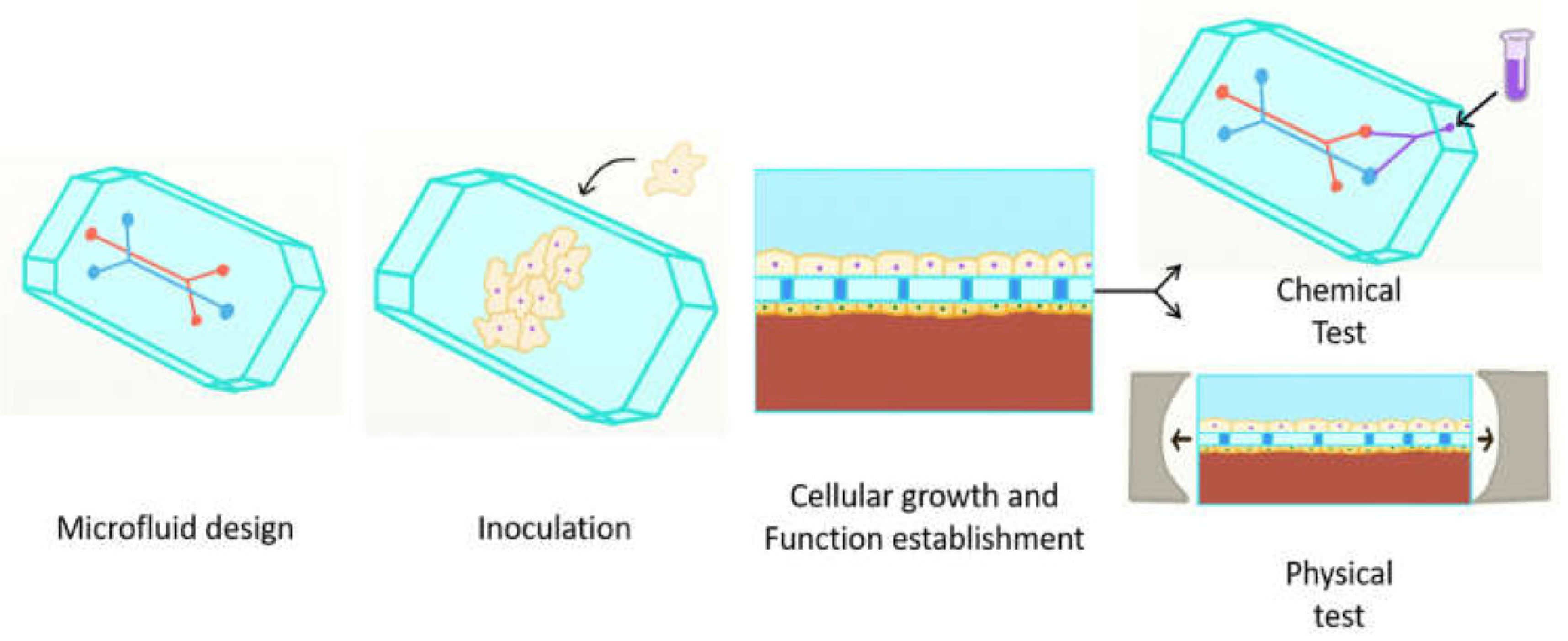
- Sosa-Hernández, J.E.; Villalba-Rodríguez, A.M.; Romero-Castillo, K.D.; Aguilar-Aguila-Isaías, M.A.; García-Reyes, I.E.; Hernández-Antonio, A.; Ahmed, I.; Sharma, A.; Parra-Saldívar, R.; Iqbal, H.M.N. Organs-on-a-Chip Module: A Review from the Development and Applications Perspective. Micromachines 2018, 9, 536. [Google Scholar] [CrossRef]
- Villanueva, L.G.; Bausells, J.; Brugger, J. Grand Challenge in N/MEMS. Front. Mech. Eng. 2016, 1, 15. [Google Scholar] [CrossRef]
- Hopcroft, M.A.; Nix, W.D.; Kenny, T.W. What is the Young’s Modulus of Silicon? J. Microelectromech. Syst. 2010, 19, 229–238. [Google Scholar] [CrossRef]
- Council, N.R. Microelectromechanical Systems: Advanced Materials and Fabrication Methods; National Academies Press: Washington, DC, USA, 1998. [Google Scholar]
- Ionov, L. Hydrogel-based actuators: Possibilities and limitations. Mater. Today 2014, 17, 494–503. [Google Scholar] [CrossRef]
- Partership, P.F. An Introduction to MEMS; Prime Faraday Partnership: Loughborough, UK, 2002. [Google Scholar]
- Blachowicz, T.; Ehrmann, A. 3D Printed MEMS Technology—Recent Developments and Applications. Micromachines 2020, 11, 434. [Google Scholar] [CrossRef] [PubMed]
- Lee, S.; Jen, K.; Willson, C.G.; Byers, J.; Zimmerman, P.; Turro, N. Materials modeling and development for use in double-exposure lithography applications. J. Micro/Nanolithogr. MEMS MOEMS 2009, 8, 011011. [Google Scholar] [CrossRef][Green Version]
- Arbabi, E.; Arbabi, A.; Kamali, S.M.; Horie, Y.; Faraji-Dana, M.; Faraon, A. MEMS-tunable dielectric metasurface lens. Nat. Commun. 2018, 9, 812. [Google Scholar] [CrossRef] [PubMed]
- Pattanaik, P.; Ojha, M. Review on challenges in MEMS technology. Mater. Today Proc. 2021, in press. [Google Scholar] [CrossRef]
- Crone, W.C.; Sharpe, W. A brief introduction to MEMS and NEMS. In Springer Handbook of Experimental Solid Mechanics; Springer: New York, NY, USA, 2008; pp. 203–228. [Google Scholar]


| Micropump Type | Driving Mechanism | Advantages | Disadvantages |
|---|---|---|---|
| electrostatic | electrostatic forces due to membrane bending |
|
|
| piezoelectric | pump chamber deformation due to piezoelectric element motion |
| - |
| thermo-pneumatic | intermittent compression and expansion of an air compartment due to a cyclic use of a twosome heater and cooler | - | - |
| bimetallic | intermittent compression and expansion due to repeated heating and cooling of two materials with different thermal expansion coefficients |
|
|
| shape-memory alloy | phase alteration inside two solid phases |
| - |
| ionic conductive polymeric films | electric field-generated stress gradient of the ionic movement | - |
|
| electrochemical | reversible electrochemical reactions for gas bubble expansion and electrolysis reduction in the aqueous electrolyte solution |
|
|
| electrohydrodynamic | interaction of electrostatic forces with ions within dielectric fluids | - | - |
| electrowetting | changes of the surface energy of a conductive liquid in contact with a dielectric-coated electrode when an external voltage potential is applied |
|
|
| electro-osmotic | movement of the uncharged liquid relative to the charged microchannel surfaces under the action of an externally applied electric field |
|
|
| magnetohydrodynamic | movement of electrically or weakly electrically conductive liquids by the Ampère’s force | - | - |
Publisher’s Note: MDPI stays neutral with regard to jurisdictional claims in published maps and institutional affiliations. |
© 2022 by the authors. Licensee MDPI, Basel, Switzerland. This article is an open access article distributed under the terms and conditions of the Creative Commons Attribution (CC BY) license (https://creativecommons.org/licenses/by/4.0/).
Share and Cite
Chircov, C.; Grumezescu, A.M. Microelectromechanical Systems (MEMS) for Biomedical Applications. Micromachines 2022, 13, 164. https://doi.org/10.3390/mi13020164
Chircov C, Grumezescu AM. Microelectromechanical Systems (MEMS) for Biomedical Applications. Micromachines. 2022; 13(2):164. https://doi.org/10.3390/mi13020164
Chicago/Turabian StyleChircov, Cristina, and Alexandru Mihai Grumezescu. 2022. "Microelectromechanical Systems (MEMS) for Biomedical Applications" Micromachines 13, no. 2: 164. https://doi.org/10.3390/mi13020164
APA StyleChircov, C., & Grumezescu, A. M. (2022). Microelectromechanical Systems (MEMS) for Biomedical Applications. Micromachines, 13(2), 164. https://doi.org/10.3390/mi13020164