Communication

Fabrication and Properties of InGaZnO Thin-Film Transistors Based on a Sol–Gel Method with Different Electrode Patterns

Key Laboratory of Architectural Cold Climate Energy Management, Ministry of Education, School of Electronics and Computer, Jilin Jianzhu University, 5088 Xincheng Street, Changchun 130118, China
*
Authors to whom correspondence should be addressed.
Micromachines 2022, 13(12), 2207; https://doi.org/10.3390/mi13122207
Submission received: 29 November 2022 / Revised: 12 December 2022 / Accepted: 12 December 2022 / Published: 13 December 2022
(This article belongs to the Special Issue Recent Advances in Thin Film Transistors)

Abstract

:
The preparation of thin-film transistors (TFTs) with InGaZnO (IGZO) channels using sol–gel technology has the advantages of simplicity in terms of process and weak substrate selectivity. We prepared a series of TFT devices with a top contact and bottom gate structure, in which the top contact was divided into rectangular and circular structures of drain/source electrodes. The field-effect performance of TFT devices with circular pattern drain/source electrodes was better than that with a traditional rectangular structure on both substrates. The uniform distribution of the potential in the circular electrode structure was more conducive to the regulation of carriers under the same channel length at different applied voltages. In addition, with the development of transparent substrate devices, we also constructed a hafnium oxide (HfO2) insulation layer and an IGZO active layer on an indium tin oxide conductive substrate, and explored the effect of circular drain/source electrodes on field-effect properties of the semitransparent TFT device. The IGZO deposited on the HfO2 dielectric layer by spin-coating can effectively reduce the surface roughness of the HfO2 layer and optimize the scattering of carriers at the interface in TFT devices.

1. Introduction

With the gradual upgrading of electronic devices, the performance of display components should also meet the demand of the industry, among which thin-film transistors (TFTs) are an important part of screen display with broad application prospects [1,2,3]. The low-cost, highly reliable, and low-power-consumption TFTs in functional integrated circuits have received increasing attention, and the material selection and structure design of each functional layer in devices are further improved to enhance field-effect properties [4,5,6,7,8]. Metal oxides [9,10,11,12,13,14] and organic semiconductors [15,16,17] are two promising classes of TFT channel materials that have made impressive progress in TFT devices compared to traditional silicon. Organic active-layer TFTs offer potential use in large-area electronic display devices [18,19]. However, inorganic channel layers can maintain good thermal and electrical stability and avoid affecting the device performance caused by the degradation of material itself during long operation cycles [20,21]. Moreover, metal oxide TFTs are developed mainly for display driven applications, due to their advantages of stable material properties, controllable element doping, and simple preparation process [22].
Among metal oxide semiconductors, the amorphous InGaZnO (IGZO) system is especially promising for use as a high-performance TFT active material. Because the indium as a doping cation affects the electronic configuration in channel layers, and the stability of the gallium–oxygen bond suppresses the generation of oxygen vacancies, thus decreasing the free electron concentration [9,23,24,25]. The traditional preparation method of the metal oxide active layer relies on vacuum deposition technology [26]. Although sputtering deposition is beneficial to the quality of films, it cannot meet the demand of the current device fabrication process simplification. Sol–gel technology has the advantages of low cost, diversified choices of doping materials, and controllable component ratio in a simple preparation process [27]. Moreover, the metal oxide films prepared by spin-coating method have a wide selection of substrates [28]. The premise is to improve the wetting of the precursor solution onto the target substrates [29].
Different types of TFTs were formed by spin-coating IGZO on a traditional Si/SiO2 substrate and a transparent substrate composed of an indium tin oxide (ITO) film and a hafnium dioxide (HfO2) as the bottom gate and insulation layer. Transparent metal oxide TFTs have been widely studied in wearable electronic devices and smart displays [30]. Moreover, with the improvement in the performance of TFT devices, the circular electrode structure should be explored to break the traditional rectangular symmetrical structure in TFTs. The circular electrode structure can solve the difference of electric field distribution between electrode centers and electrode edges compared with a traditional rectangular symmetrical structure. In this study, a spin-coating process that can prepare InGaZnO channel and also reduce the roughness of the interface between the active and the dielectric layer for TFTs was reported. A TFT structure with a bottom gate consisting of Si wafers or ITO conductive glass and a top contact consisting of rectangular symmetrical and circular drain/source electrodes was constructed to analyze the difference in electrical properties of TFT devices. In addition, the introduction of circular drain/source electrodes to optimize the uniformity of electric field distribution and the field-effect parameters was investigated.

2. Materials and Methods

2.1. Preparation of TFT Devices

In this paper, the commercial ITO conductive glass (HNXC Tech Co., Ltd., Shenzhen, China) with transmittance of 86% and surface resistance of 11 ohm/sq was used as the bottom electrode of TFTs. A hafnium dioxide (HfO2) layer as dielectric layer with a thickness of ~170 nm was deposited on the ITO substrate by rf magnetron sputtering for 120 min in argon atmosphere. The growth conditions were set as growth pressure of 8 mTorr, sputtering power of 150 W, and distance between substrate and sputtering target of 100 mm. A Si wafer with a SiO2 thickness of 285 nm from HEFEI KEJING Materials Tech Co., Ltd. (Hefei, China) as the bottom gate and insulation layer was used for contrast with the transparent substrates. The colloidal precursors were prepared from indium nitrate (99.99%), gallium nitrate (99.99%), and zinc acetate (99.99%) dissolved in 5 mL of methyl glycol from Shanghai Aladdin Biochemical Technology Co. Ltd. (Shanghai, China) to achieve IGZO solutions with indium, gallium, and zinc molar ratios of 2:1:7. The active layers were prepared by the spin-coating method. The argon plasma was used to remove adsorbed impurities on the substrate surface before a spin-coating process. The purpose was to reduce the thickness of the active layer and form a shorter path for carrier migration. The plasma processing conditions were set as power supply of 75 W and processing time of 10 s. The spin-coating conditions were set as spin speed of 3000 r/min and duration of 30 s. Then, the samples were placed on the hot plate and heated at 90 °C for 3 min to cure the deposited colloid. The active layer was heated to 550 °C at a heating rate of 5 °C/s with air atmosphere in a rapid annealing furnace and kept for 60 min. The thickness of IGZO active layer after annealing treatment was 40 ± 5 nm. A schematic of structure of the IGZO TFTs on the Si/SiO2 and ITO/HfO2 substrates with rectangular symmetrical and circular drain/source electrodes is shown in Figure 1. The rectangular-patterned active layer and drain/source electrodes were obtained by lithography. The circular electrode structure was obtained by mask evaporation on the prepared IGZO channel layer using an electron beam evaporation system. The rectangular and circular drain/source electrodes were the evaporation layer of aluminum metal with a thickness of ~50 nm. The rectangular channel pattern has a length of ~100 μm and a width of ~300 μm. The channel length of circular pattern TFT devices is also about ~100 μm.

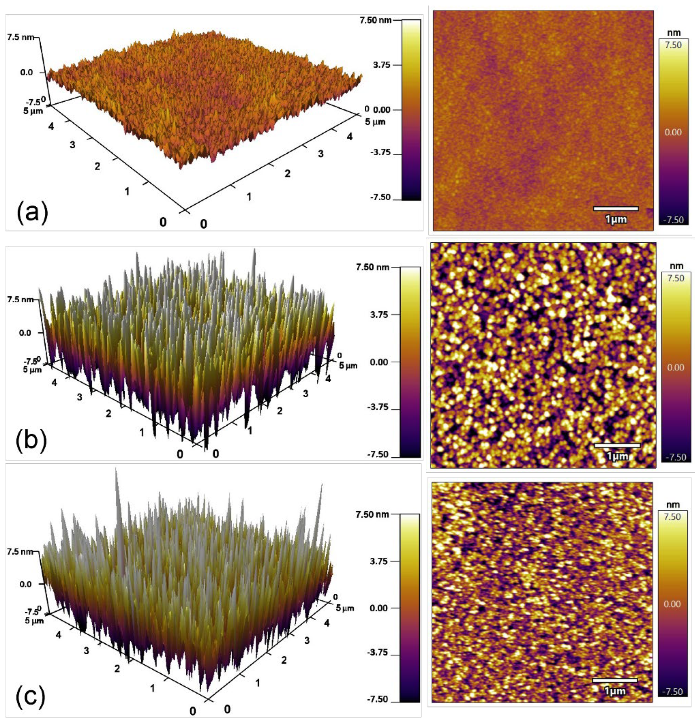
2.2. Characterization

The active layers were obtained by a spin-coater (SPS Spin150i, SPS Company, Bienenbuttel, Germany). The microscope images of the rectangular and circular channel patterns were obtained by a Zeiss microscope (AxioScope A1, Carl Zeiss AG). The IGZO active layers were annealed in air atmospheres using a vacuum rapid annealing furnace (RTP-100, UniTemp, Pfaffenhofen, Germany). The dielectric layers were prepared by rf magnetron sputtering (PVD75, Kurt. J. Lesker Company, Jefferson Hills, PA, USA). The rectangular patterned drain/source electrodes and ac-tive layers are graphically etched with a photolithography system (ABM/6/350/NUV/DCCD/M, ABM, Inc., New York, NY, USA). The surface morphology and roughness of active and dielectric layers were characterized by an atomic force microscope (MFP-3D Origin+, Oxford Instruments, Abingdon, UK). The field-effect parameters were measured by a semiconductor parameter measuring instrument (B1500A, Keysight Technologies, Santa Rosa, CA, USA).

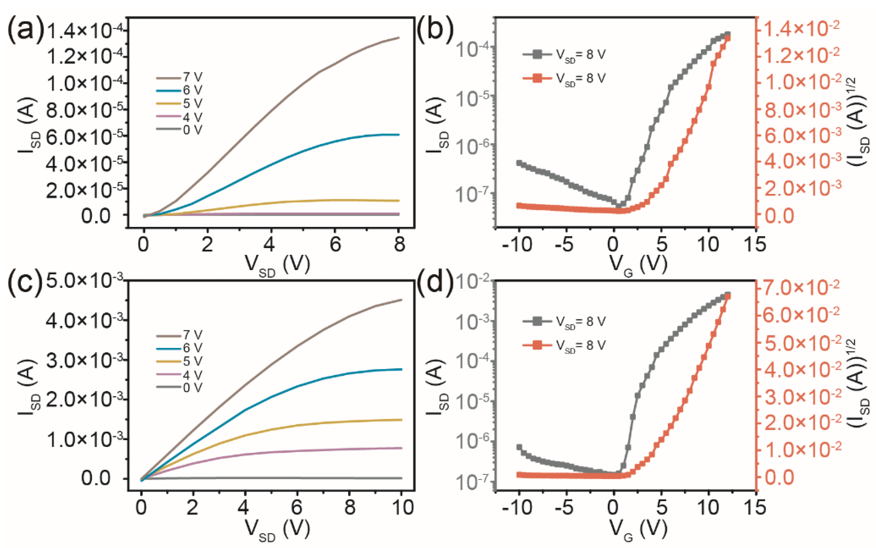
3. Results and Discussion

The IGZO channel layer was first deposited on Si/SiO2 substrates via a spin-coating process using the IGZO precursor solution. The prepared IGZO film was then annealed at 550 °C, lithographed, and covered with aluminium electrodes to obtain a TFT device with a rectangular channel pattern. The channel length and width of the IGZO/SiO2/Si TFT were about 100 μm and 300 μm, respectively. The pristine IGZO channel layer needed to be annealed to remove organic impurities and improve the film quality. The thickness of the prepared IGZO channel layer was about 40 ± 5 nm. The drain current (ISD) vs. drain-source voltage (VSD) output characteristics of TFTs with rectangular channel patterns at gate voltages (VG) from 0 to 40 V is shown in Figure 2a. The curves show the typical n-type TFT performance with the clear transition from linear to saturation behavior. The threshold voltage (VT) was estimated by extrapolating the linear portion of the (ISD)1/2 vs. VG curves at VSD = 20 V in the typical transfer curves of the TFT device with symmetrical rectangular electrodes. The TFT with rectangular pattern channel on a Si/SiO2 substrate exhibited an on/off ratio (Ion/Ioff) of 2.61 × 10⁴ and a VT of 13.5 V. The value of field-effect mobility (μ) can reflect the carrier migration ability of a semiconductor under different electric fields [31]. The μ in the saturation region was evaluated from the following relationship:
μ = 2 L WC i ( I SD V G ) 2
where L and W are the channel length and width of the IGZO/SiO2/Si TFT with a rectangular channel pattern, respectively, and Ci is the capacitance per unit area of the SiO2 gate insulator with a thickness of about 285 nm. By substituting these parameters into Equation (1), a μ value was obtained for the TFT with a rectangular channel pattern of 0.021 cm2/Vs.
In contrast, the IGZO/SiO2/Si TFT device with the circular drain/source electrodes achieves higher ISD in the output characteristic curves, as shown in Figure 2c. The reason is that the carrier injection with circular electrodes in the IGZO channel layers can effectively solve the problem of uneven electric field distribution between the electrode center and edge in traditional symmetrical rectangular structures. The uniform distribution of VSD is more conducive to carrier injection and migration in the channel. The Ion/Ioff and the VT estimated by extrapolating the linear portion of the (ISD)1/2 vs. VG curves at VSD = 20 V in the transfer characteristics of the TFT device with circular channel patterns can be calculated as shown in Figure 3d. It can be seen that the Ion/Ioff and VT of the TFT device with circular channel patterns are significantly improved, and the values are 2.04 × 10⁶ and 7.2 V, respectively. For circular drain/source electrodes (as shown in Figure 1c), R1 is the radius of the internal source electrode (~500 μm) and R2 is the sum of the radius of the internal source electrode and the length of the IGZO channel (~500 + 100 μm) used to calculate the channel width to length ratio (W/L) of TFTs with circular channel patterns, as a function of the W/L change, according to [32]:
W / L = 2 π ln ( R 2 / R 1 )
In addition, the value of μ of the IGZO/SiO2/Si TFT device with circular electrodes was 0.104 cm2/Vs by substituting Equation (2) into Equation (1). The increase in μ can be conducive to improving the switching speed of TFT devices.
With the rapid development of a transparent or translucent display field, the demand for transparent TFTs has gradually increased, and the gate and dielectric layers as the key points of the display driver industry have attracted more attention. In this paper, the ITO transparent conductive films were used as bottom gate electrodes. In addition, the HfO2 with high dielectric constant deposited by magnetron sputtering can be selected as the dielectric layer for TFT devices. Similarly, the TFT devices with IGZO channel layers and rectangular and circular drain/source electrodes were prepared on ITO/HfO2 substrates, and the output and transfer characteristic curves of the TFTs were characterized as shown in Figure 3. The transition from the linear to the saturation part and the good regulation of the ISD are both obtained in the output characteristic curves of the TFTs with rectangular and circular channel patterns under VG from 0 to 7 V, as shown in Figure 3a,c. The curves show typical n-type transistor performance. However, due to the high conductivity of ITO and the weak compactness of HfO2 grown by sputtering at room temperature, a higher ISD and lower applied VSD of the IGZO/HfO2/ITO TFTs than those on the traditional Si/SiO2 substrates were obtained. The slope value of the (ISD)1/2 vs. VG curves at VSD = 8 V will be increased for the TFTs with ITO/HfO2 substrates, resulting in an increase in estimated μ values. Figure 3b,d show the typical transfer curves ISD–VG and (ISD)1/2–VG at VSD = 8 V of the IGZO/HfO2/ITO TFT device with rectangular and circular channel patterns, respectively. The value of μ was derived from a linear fit to the plot of the square root of ISD vs. VG. The TFT device with rectangular symmetric drain/source electrodes on ITO/HfO2 substrates exhibited a VT of 4.4 V, an Ion/Ioff of 3.30 × 10³, and a μ of 18.49 cm2/Vs. In contrast, a TFT device with the circular channel patterns on the same substrate also showed better field-effect parameters, including a VT of 4.1 V, an Ion/Ioff of 2.85 × 10⁴, and a μ of 39.19 cm2/Vs. The mobility values reported by different studies are summarized in Table 1. There is a gap between the performance of IGZO TFTs with rectangular and circular channel patterns in this work compared with typical TFTs, but we will improve the electrical properties and stability of the TFT devices and the tolerance of TFTs on ITO substrates to high applied voltage from the perspective of interface modification in the next work.
In the above, we discussed the variation of electrical performance of IGZO TFT devices on different substrates and with different patterns of drain/source electrodes. For the IGZO channel layer deposited by a spin-coating method, besides the advantage of a simple preparation process, the effect of the spin-coating on surface roughness of the channel layers should also be investigated. In Figure 4, the variation of the IGZO and HfO2 surface morphologies on different substrates was analyzed by atomic force microscope. As shown in Figure 4a, the IGZO channel layer by spin-coating on a Si/SiO2 substrate has a relatively flat surface with a roughness of 0.796 nm. The very low surface roughness benefited from the preparation of the channel layer from the precursor of the ionic solution. The HfO2 layer by magnetron sputtering on the ITO conductive glass has a rougher surface with a roughness of 4.460 nm, as shown in Figure 4b. However, the roughness of the HfO2 layer after coating the IGZO channel layer was reduced to 3.797 nm, as shown in Figure 4c. This is because the IGZO precursor solution can be effectively filled into the surface micro-porous structure of the HfO2 layer during spin-coating. Reducing the roughness of the surface helps decrease the scattering of carriers at the interface and further improves the transport capacity of carriers in the channel of TFT devices.

4. Conclusions

The field-effect performance of the IGZO TFT device with symmetrical rectangular and circular channel patterns on different substrates was investigated in this paper. The electrical properties of TFT devices with circular drain/source electrodes were better than those with a traditional rectangular structure on both substrates, due to the uniform distribution of applied voltages between the electrode center and edge. The uniform distribution of the applied voltage was more conducive to carrier injection and migration in the channel. The TFT with rectangular and circular channel patterns on the Si/SiO2 showed a VT value of 13.5 V and 7.2 V, an Ion/Ioff value of 2.61 × 10⁴ and 2.04 × 10⁶, and a μ value of 0.021 cm2/Vs and 0.104 cm2/Vs, respectively. A high dielectric constant HfO2 layer on an ITO transparent conductive film was used as the bottom gate and dielectric layer in IGZO TFT devices. The surface roughness of the HfO2 layer by sputtering deposition on the ITO can be effectively reduced by spin-coating the IGZO channel layer. This improved interface contact quality will effectively decrease the scattering of carriers at the interface. The TFT with rectangular and circular channel patterns on the ITO/HfO2 showed a VT value of 4.4 V and 4.1 V, an Ion/Ioff value of 3.30 × 10³ and 2.85 × 10⁴, and a μ value of 18.49 cm2/Vs and 39.19 cm2/Vs, respectively. In the next work, we plan to use transparent metal oxides or metal grids as the drain/source electrodes to solve the problem of full transparency of TFT devices.

Author Contributions

Conceptualization, X.Y. (Xingzhen Yan) and B.L.; methodology, X.Y. (Xingzhen Yan), B.L., K.S. and Y.Z.; formal analysis, B.L. and K.S.; investigation, Y.W., F.Y. and C.W.; writing—original draft preparation, X.Y. (Xingzhen Yan) and B.L.; writing—review and editing, X.Y. (Xingzhen Yan) and X.Y. (Xiaotian Yang); project administration, Y.C. and X.Y. (Xiaotian Yang); funding acquisition, X.Y. (Xingzhen Yan). All authors have read and agreed to the published version of the manuscript.

Funding

This research was funded by the Science and Technology Development Project of Jilin Province, China (Nos.YDZJ202201ZYTS396, JJKH20220271KJ, and 20200401012GX).

Data Availability Statement

Not applicable.

Conflicts of Interest

The authors declare no conflict of interest.

References

  1. Nomura, K.; Ohta, H.; Ueda, K.; Kamiya, T.; Hirano, M.; Hosono, H. Thin-film transistor fabricated in single-crystalline transparent oxide semiconductor. Science 2003, 300, 1269–1272. [Google Scholar] [CrossRef] [PubMed]
  2. Gelinck, G.; Huitema, H.; Veenendaal, E.; Cantatore, E.; Schrijnemakers, L.; Putten, J.; Geuns, T.; Beenhakkers, M.; Giesbers, J.; Huisman, B.; et al. Flexible active-matrix displays and shift registers based on solution-processed organic transistors. Nat. Mater. 2004, 3, 106–110. [Google Scholar] [CrossRef]
  3. Street, R.A. Thin-film transistors. Adv. Mater. 2009, 21, 2007–2022. [Google Scholar] [CrossRef]
  4. Hoffman, R.L.; Norris, B.J.; Wager, J.F. ZnO-based transparent thin-film transistors. Appl. Phys. Lett. 2003, 82, 733–735. [Google Scholar] [CrossRef]
  5. Fortunato, E.; Barquinha, P.; Pimentel, A.; Goncalves, A.; Marque, A.; Pereira, L.; Martins, R. Wide-Bandgap High-Mobility ZnO Thin-Film Transistors Produced at Room Temperature. Appl. Phys. Lett. 2004, 85, 2541–2543. [Google Scholar] [CrossRef]
  6. Dimitrakopoulos, C.D.; Purushothaman, S.; Kymissis, J.; Callegari, A.; Shaw, J.M. Low-Voltage Organic Transistors on Plastic Comprising High-Dielectric Constant Gate Insulators. Science 1999, 283, 822–824. [Google Scholar] [CrossRef] [PubMed]
  7. Tang, Y.; Huang, C.H.; Nomura, K. Vacuum-Free Liquid-Metal-Printed 2D Indium-Tin Oxide Thin-Film Transistor for Oxide Inverters. ACS Nano 2022, 16, 3280–3289. [Google Scholar] [CrossRef]
  8. Jana, S.; Martins, R.; Fortunato, E. Stacking-Dependent Electrical Transport in a Colloidal CdSe Nanoplatelet Thin-Film Transistor. Nano Lett. 2022, 22, 2780–2785. [Google Scholar] [CrossRef]
  9. Nomura, K.; Ohta, H.; Takagi, A.; Kamiya, T.; Hirano, M.; Hosono, H. Room-Temperature Fabrication of Transparent Flexible Thin-Film Transistors Using Amorphous Oxide Semiconductors. Nature 2004, 432, 488–492. [Google Scholar] [CrossRef]
  10. Fortunato, E.; Barquinha, P.; Martins, R. Oxide Semiconductor Thin-Film Transistors: A Review of Recent Advances. Adv. Mater. 2012, 24, 2945–2986. [Google Scholar] [CrossRef]
  11. Banger, K.K.; Yamashita, Y.; Mori, K.; Peterson, R.L.; Leedham, T.; Rickard, J.; Sirringhaus, H. Low-temperature, high-performance solution-processed metal oxide thin-film transistors formed by a ‘sol–gel on chip’ process. Nat. Mater. 2011, 10, 45–50. [Google Scholar] [CrossRef] [PubMed]
  12. Islam, M.M.; Saha, J.K.; Hasan, M.M.; Kim, J.; Bukke, R.N.; Ali, A.; Jang, J. Spray-Pyrolyzed High-k Zirconium-Aluminum-Oxide Dielectric for High Performance Metal-Oxide Thin-Film Transistors for Low Power Displays. Adv. Mater. Interfaces 2021, 8, 2100600. [Google Scholar] [CrossRef]
  13. Ozer, E.; Kufel, J.; Myers, J.; Biggs, J.; Brown, G.; Rana, A.; Sou, A.; Ramsdale, C.; White, S. A hardwired machine learning processing engine fabricated with submicron metal-oxide thin-film transistors on a flexible substrate. Nat. Electron. 2020, 3, 419–425. [Google Scholar] [CrossRef]
  14. Liu, J.; Liu, S.; Yu, Y.; Chen, H.; Wang, C.; Su, J.; Liu, C.; Zhang, Y.; Han, J.; Shao, G.; et al. High Mobility and Photo-Bias Stable Metal Oxide Thin-Film Transistors Engineered by Gradient Doping. Adv. Electron. Mater. 2022, 8, 2100984. [Google Scholar] [CrossRef]
  15. Crone, B.; Dodabalapur, A.; Lin, Y.Y.; Filas, R.W.; Bao, Z.; LaDuca, A.; Sarpeshkar, R.; Katz, H.E.; Li, W. Large-Scale Complementary Integrated Circuits based on Organic Transistors. Nature 2000, 403, 521–523. [Google Scholar] [CrossRef]
  16. Yuan, Y.; Giri, G.; Ayzner, A.L.; Zoombelt, A.P.; Mannsfeld, S.C.; Chen, J.; Nordlund, D.; Toney, M.F.; Huang, J.; Bao, Z. Ultra-high mobility transparent organic thin film transistors grown by an off-centre spin-coating method. Nat. Commun. 2014, 5, 3005. [Google Scholar] [CrossRef] [Green Version]
  17. Guo, E.; Xing, S.; Dollinger, F.; Hubner, R.; Wang, S.J.; Wu, Z.; Leo, K.; Kleemann, H. Integrated complementary inverters and ring oscillators based on vertical-channel dual-base organic thin-film transistors. Nat. Electron. 2021, 4, 588–594. [Google Scholar] [CrossRef]
  18. Chen, Y.; Au, J.; Kazlas, P.; Ritenour, A.; Gates, H.; McCreary, M. Flexible active-matrix electronic ink display. Nature 2003, 423, 136. [Google Scholar] [CrossRef]
  19. Myny, K. The development of flexible integrated circuits based on thin-film transistors. Nat. Electron. 2018, 1, 30–39. [Google Scholar] [CrossRef]
  20. Kuribara, K.; Wang, H.; Uchiyama, N.; Fukuda, K.; Yokota, T.; Zschieschang, U.; Jaye, C.; Fischer, D.; Klauk, H.; Yamamoto, T.; et al. Organic transistors with high thermal stability for medical applications. Nat. Commun. 2012, 3, 723. [Google Scholar] [CrossRef]
  21. Rim, Y.S.; Chen, H.; Kou, X.; Duan, H.S.; Zhou, H.; Cai, M.; Kim, H.J.; Yang, Y. Boost up Mobility of Solution-Processed Metal Oxide Thin-Film Transistors via Confining Structure on Electron Pathways. Adv. Mater. 2014, 26, 4273–4278. [Google Scholar] [CrossRef] [PubMed]
  22. Yarali, E.; Koutsiaki, C.; Faber, H.; Tetzner, K.; Yengel, E.; Patsalas, P.; Kalfagiannis, N.; Koutsogeorgis, D.C.; Anthopoulos, T.D. Recent Progress in Photonic Processing of Metal-Oxide Transistors. Adv. Funct. Mater. 2019, 30, 1906022. [Google Scholar] [CrossRef] [Green Version]
  23. Yabuta, H.; Sano, M.; Abe, K.; Aiba, T.; Den, T.; Kumomi, H.; Nomura, K.; Kamiya, T.; Hosono, H. High-mobility thin-film transistor with amorphous InGaZnO4 channel fabricated by room temperature rf-magnetron sputtering. Appl. Phys. Lett. 2006, 89, 112123. [Google Scholar] [CrossRef]
  24. Nomura, K.; Takagi, A.; Kamiya, T.; Ohta, H.; Hirano, M.; Hosono, H. Amorphous oxide semiconductors for high-performance flexible thin-film transistors. Jpn. J. Appl. Phys. 2006, 45, 4303–4308. [Google Scholar] [CrossRef]
  25. Iwasaki, T.; Itagaki, N.; Den, T.; Kumomi, H.; Nomura, K.; Kamiya, T.; Hosono, H. Combinatorial approach to thin-film transistors using multicomponent semiconductor channels: An application to amorphous oxide semiconductors in In-Ga-Zn-O system. Appl. Phys. Lett. 2007, 90, 242114. [Google Scholar] [CrossRef]
  26. He, J.; Li, G.; Lv, Y.; Wang, C.; Liu, C.; Li, J.; Flandre, D.; Chen, H.; Guo, T.; Liao, L. Defect Self-Compensation for High-Mobility Bilayer InGaZnO/In2O3 Thin-Film Transistor. Adv. Electron. Mater. 2019, 5, 1900125. [Google Scholar] [CrossRef]
  27. Park, S.J.; Ha, T.J. Improved electric contact of recessed source and drain electrodes for sol-gel-based thin-film transistors consisting of amorphous ZrO2 and IGZO fabricated by microwave-annealing. Appl. Phys. Lett. 2022, 120, 153301. [Google Scholar] [CrossRef]
  28. Avis, C.; Jang, J. High-performance solution processed oxide TFT with aluminum oxide gate dielectric fabricated by a sol-gel method. J. Mater. Chem. 2011, 21, 10649–10652. [Google Scholar] [CrossRef]
  29. Seo, J.; Park, T.; Yoo, H. Systematically-optimized charge transport properties in cumulatively solution-coated zinc tin oxide and applications for complementary inverter circuits combining organic p-type transistors. Org. Electron. 2022, 107, 106567. [Google Scholar] [CrossRef]
  30. Li, Y.; Chen, T.; Ju, X.; Salim, T. Transparent electronic and photoelectric synaptic transistors based on the combination of an InGaZnO channel and a TaOx gate dielectric. Nanoscale 2022, 14, 10245–10254. [Google Scholar] [CrossRef]
  31. Horowitz, G. Organic Field-Effect Transistors. Adv. Mater. 1998, 10, 365–377. [Google Scholar] [CrossRef]
  32. Byun, Y.H.; Boer, W.D.; Yang, M.; Gu, T. An amorphous silicon TFT with annular-shaped channel and reduced gate-source capacitance. IEEE Trans. Electron Devices 1996, 43, 839–841. [Google Scholar] [CrossRef]
  33. Hwang, S.; Lee, J.H.; Woo, C.H.; Lee, J.Y.; Cho, H.K. Effect of annealing temperature on the electrical performances of solution-processed InGaZnO thin film transistors. Thin Solid Films 2011, 519, 5146–5149. [Google Scholar] [CrossRef]
  34. Wang, B.; Yu, X.; Guo, P.; Huang, W.; Zeng, L.; Zhou, N.; Chi, L.; Bedzyk, M.J.; Chang, R.P.H.; Marks, T.J.; et al. Solution-Processed All-Oxide Transparent High-Performance Transistors Fabricated by Spray-Combustion Synthesis. Adv. Electron. Mater. 2016, 2, 1500427. [Google Scholar] [CrossRef]
  35. Stallings, K.; Smith, J.; Chen, Y.; Zeng, L.; Wang, B.; Carlo, G.D.; Bedzyk, M.J.; Facchetti, A.; Marks, T.J. Self-Assembled Nanodielectrics for Solution-Processed Top-Gate Amorphous IGZO Thin-Film Transistors. ACS Appl. Mater. Interfaces 2021, 13, 15399–15408. [Google Scholar] [CrossRef]
Figure 1. Schematic illustrations of fabrication of an IGZO/SiO2/Si thin-film transistor (TFT) (a) and an IGZO/HfO2/indium tin oxide (ITO) TFT (b). Microscope images of the rectangular and circular channel patterns of an IGZO/SiO2/Si TFT (c) and an IGZO/HfO2/ITO TFT. I, II, III, and Ⅳ are four parts of the circular channel pattern (d). The scale bar is 200 μm.
Micromachines 13 02207 g001
Figure 2. Output characteristics and transfer characteristics of TFTs with rectangular channel patterns (a,b) and circular channel patterns (c,d) on the Si/SiO2 substrates.
Micromachines 13 02207 g002
Figure 3. Output characteristics and transfer characteristics of TFTs with rectangular channel patterns (a,b) and circular channel patterns (c,d) on ITO/HfO2 substrates.
Micromachines 13 02207 g003
Figure 4. Atomic force microscope images of the IGZO channel layer on the Si/SiO2 substrate (a), the HfO2 dielectric layer deposited on the ITO (b), and the IGZO channel layer on the ITO/HfO2 substrate (c).
Micromachines 13 02207 g004
Table 1. Mobility values of the IGZO TFTs with different substrates and dielectric layers.
TypeMobility (cm2/Vs)Ref.
Solution-processed IGZO on Si/SiO2 substrates6.41[33]
Solution-processed IGZO on ITO substrates (all-oxide transparent TFTs)8[34]
Solution-processed IGZO with self-assembled nanodielectrics19.4[35]
Solution-processed IGZO on Si/SiO2 substrates with circular channel patterns0.104Our result
Solution-processed IGZO on ITO substrates with circular channel patterns39.19Our result
Publisher’s Note: MDPI stays neutral with regard to jurisdictional claims in published maps and institutional affiliations.

