
Ultrafast Temporal-Spatial Dynamics of Phase Transition in N-Doped Ge2Sb2Te5 Film Induced by Femtosecond Laser Pulse Irradiation


Abstract
1. Introduction
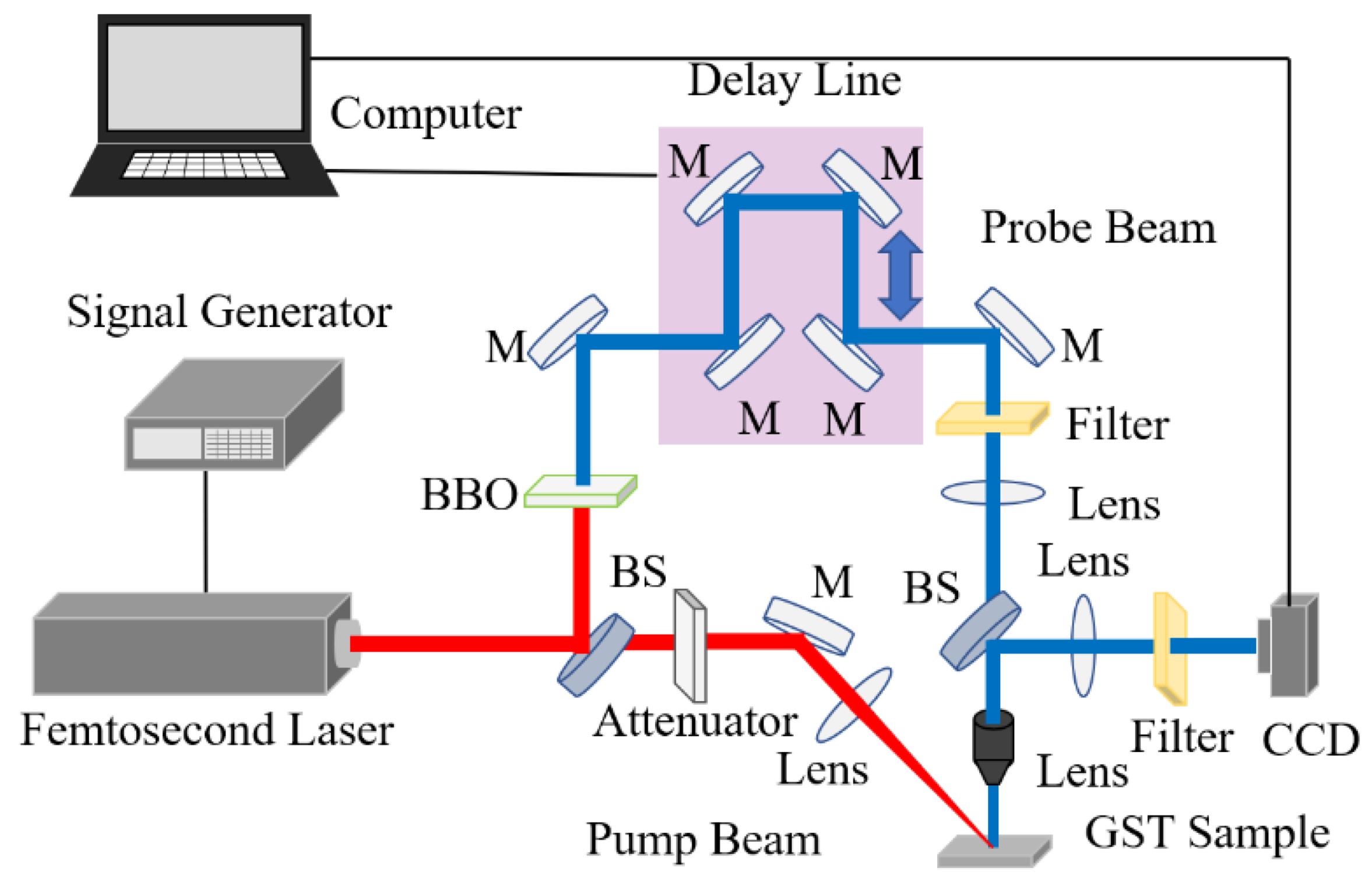
2. Experiment
3. Results and Discussion
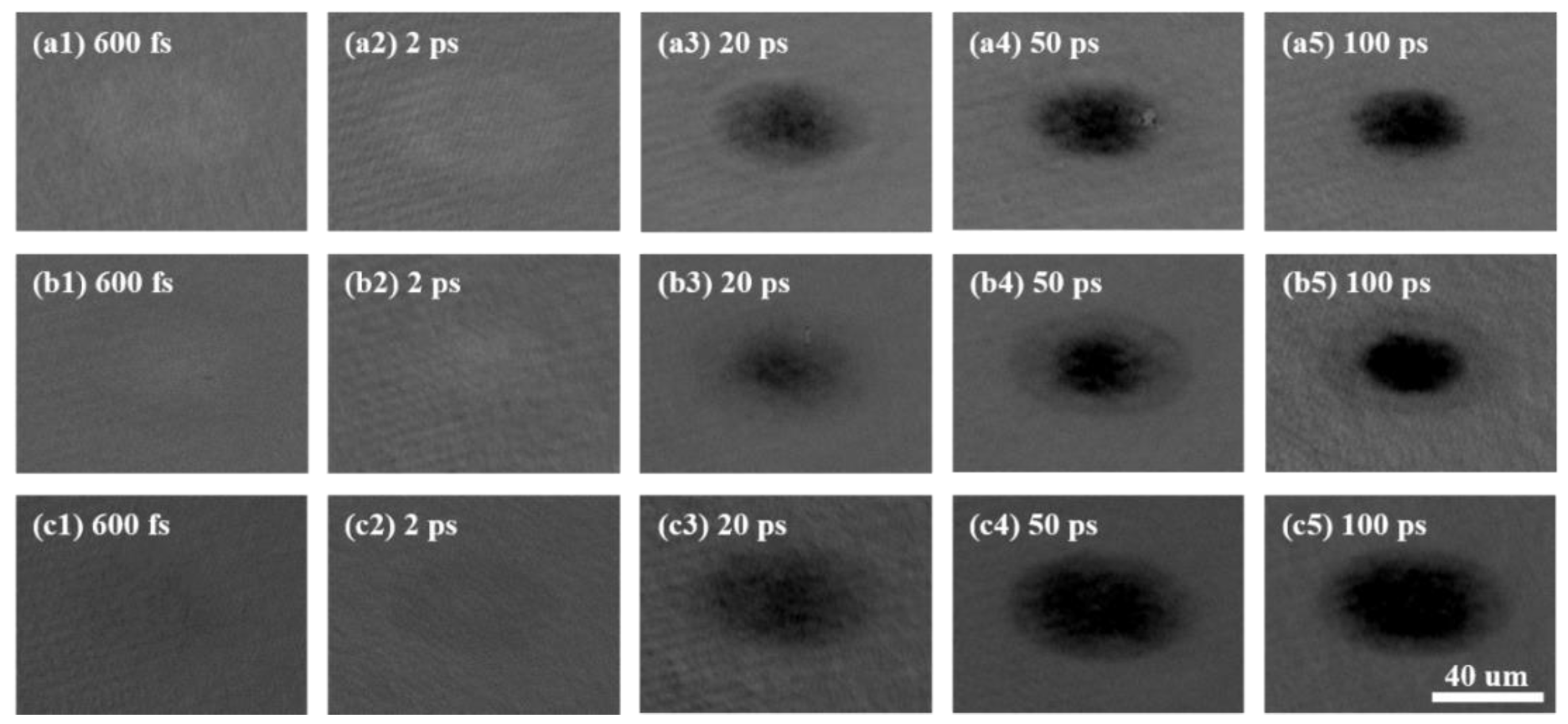
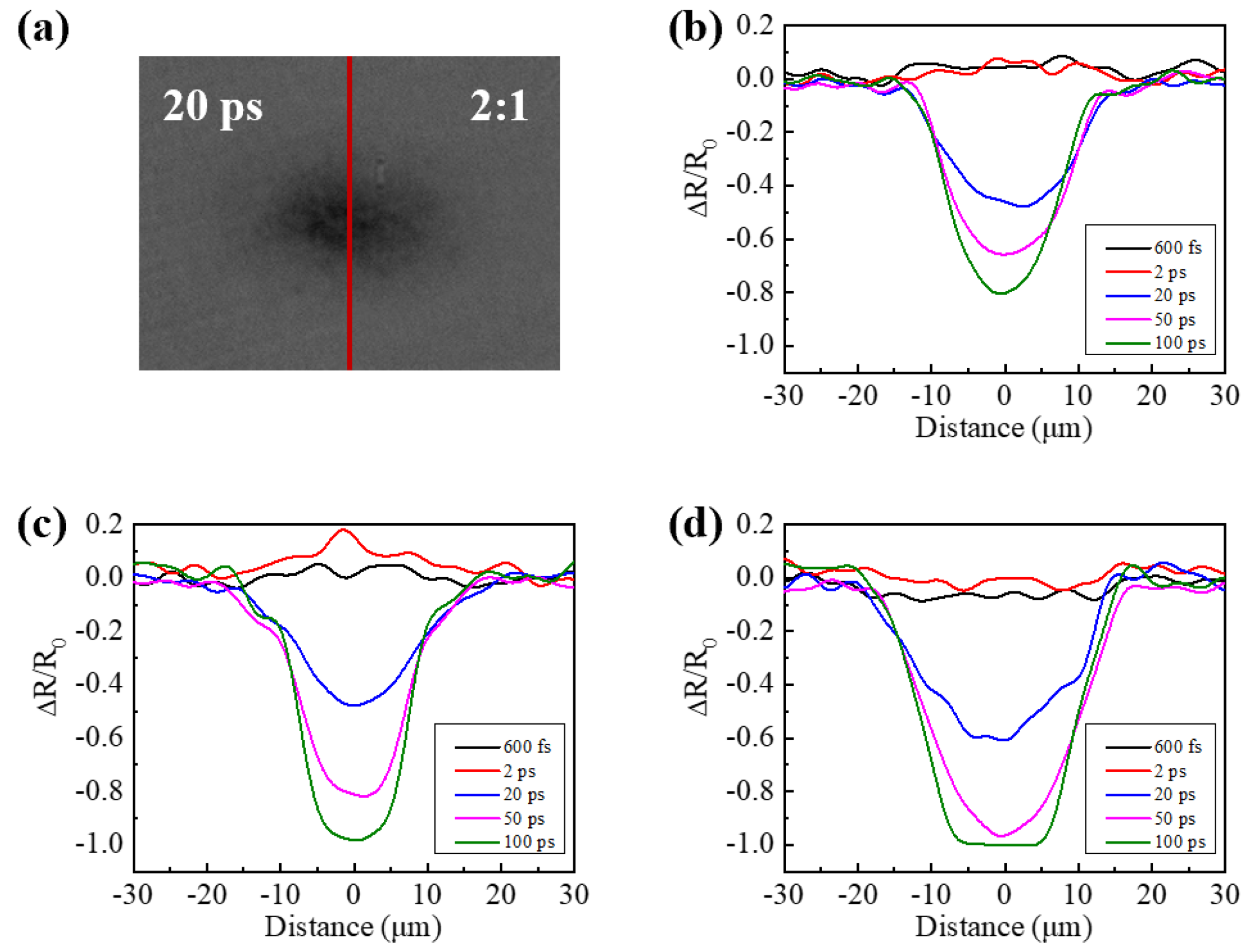
3.1. Spatial-Temporal Resolved Measurement of Femtosecond Laser Pulses Exciting Three Kinds of Films
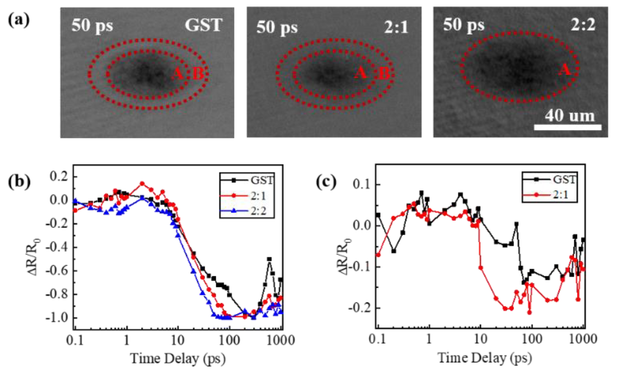
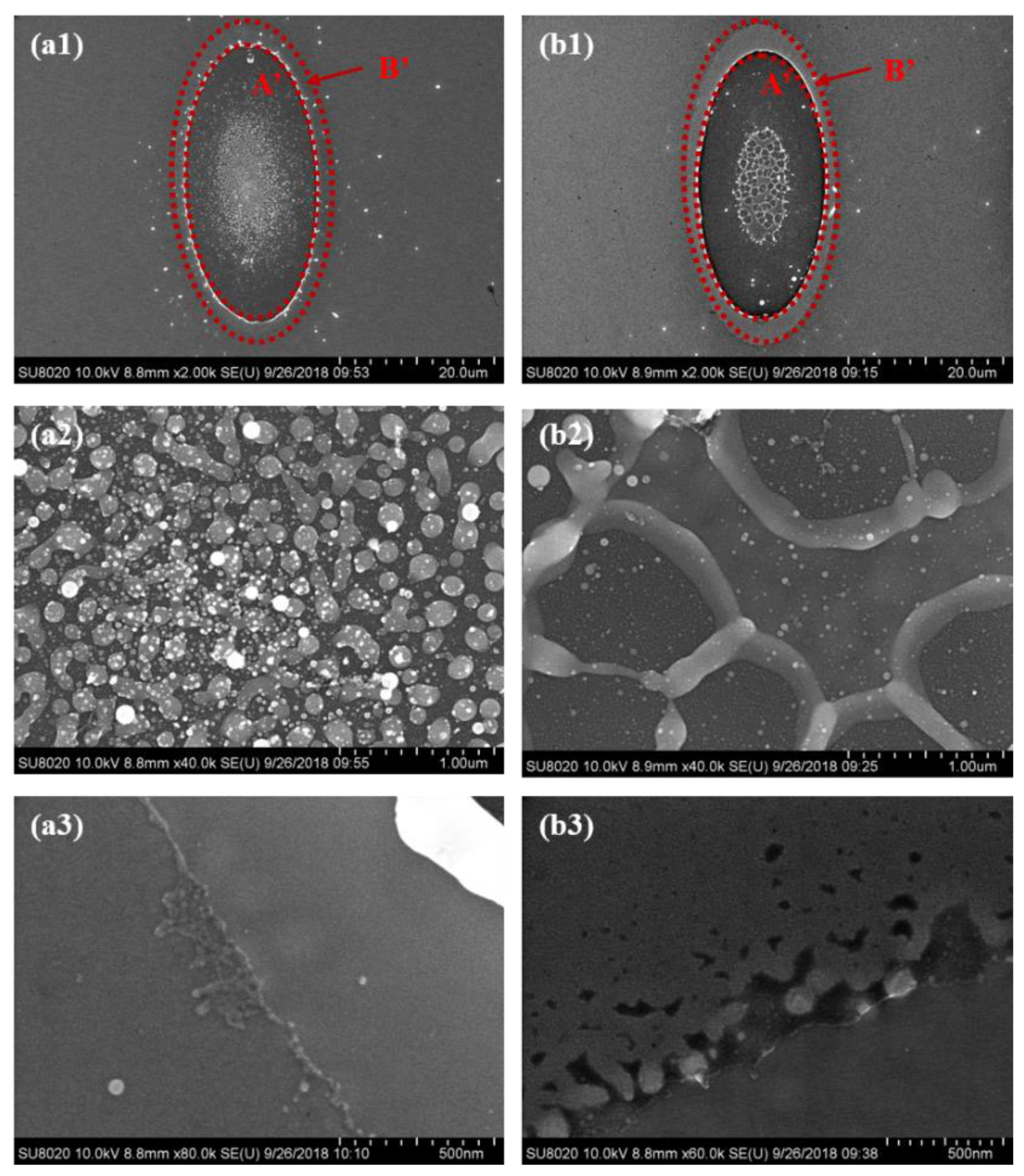
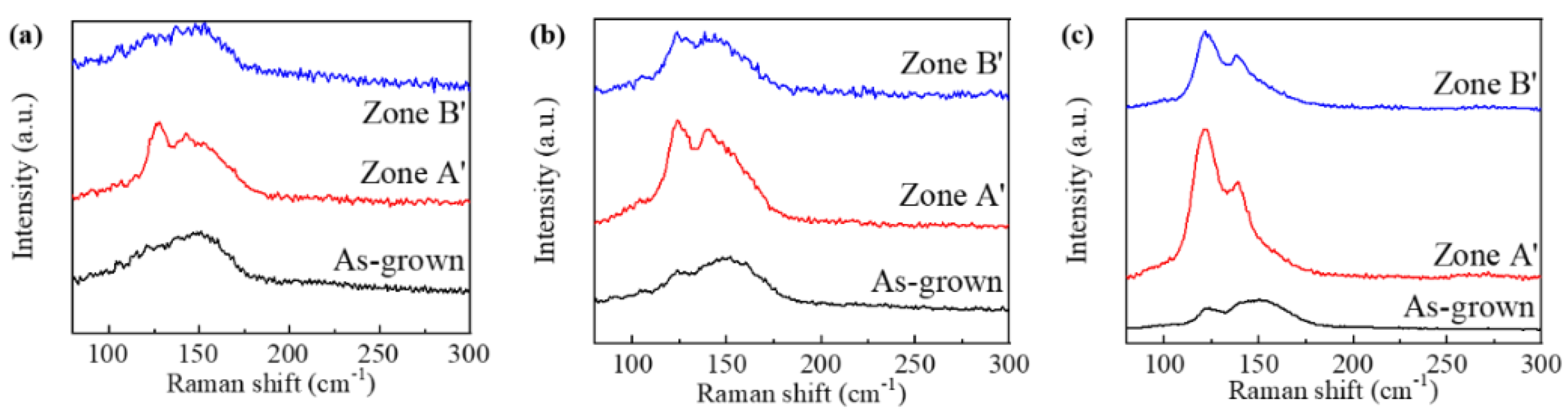
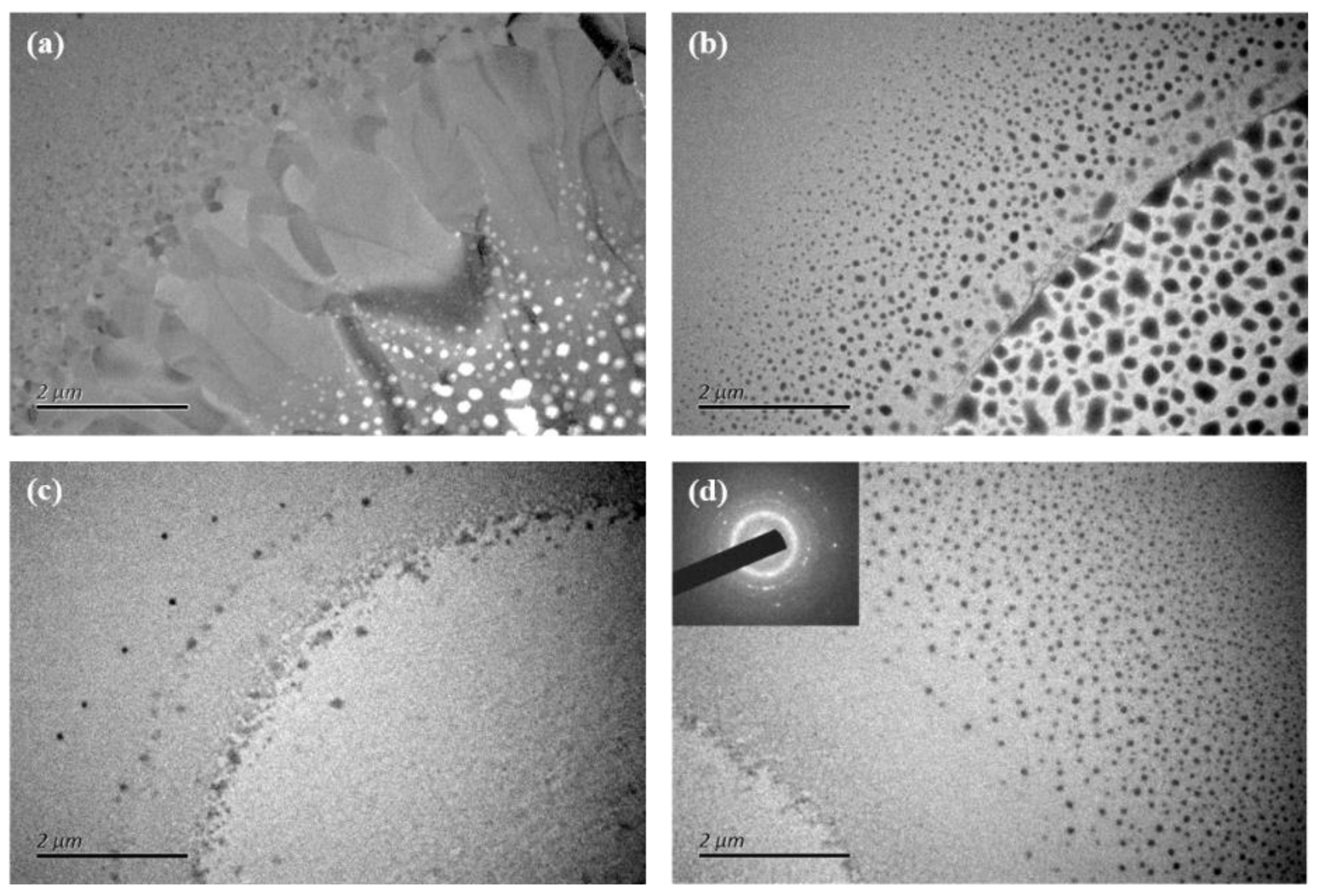
3.2. Morphology Distribution and Crystallization Characterization of the Irradiation Regions for Three Kinds of Films
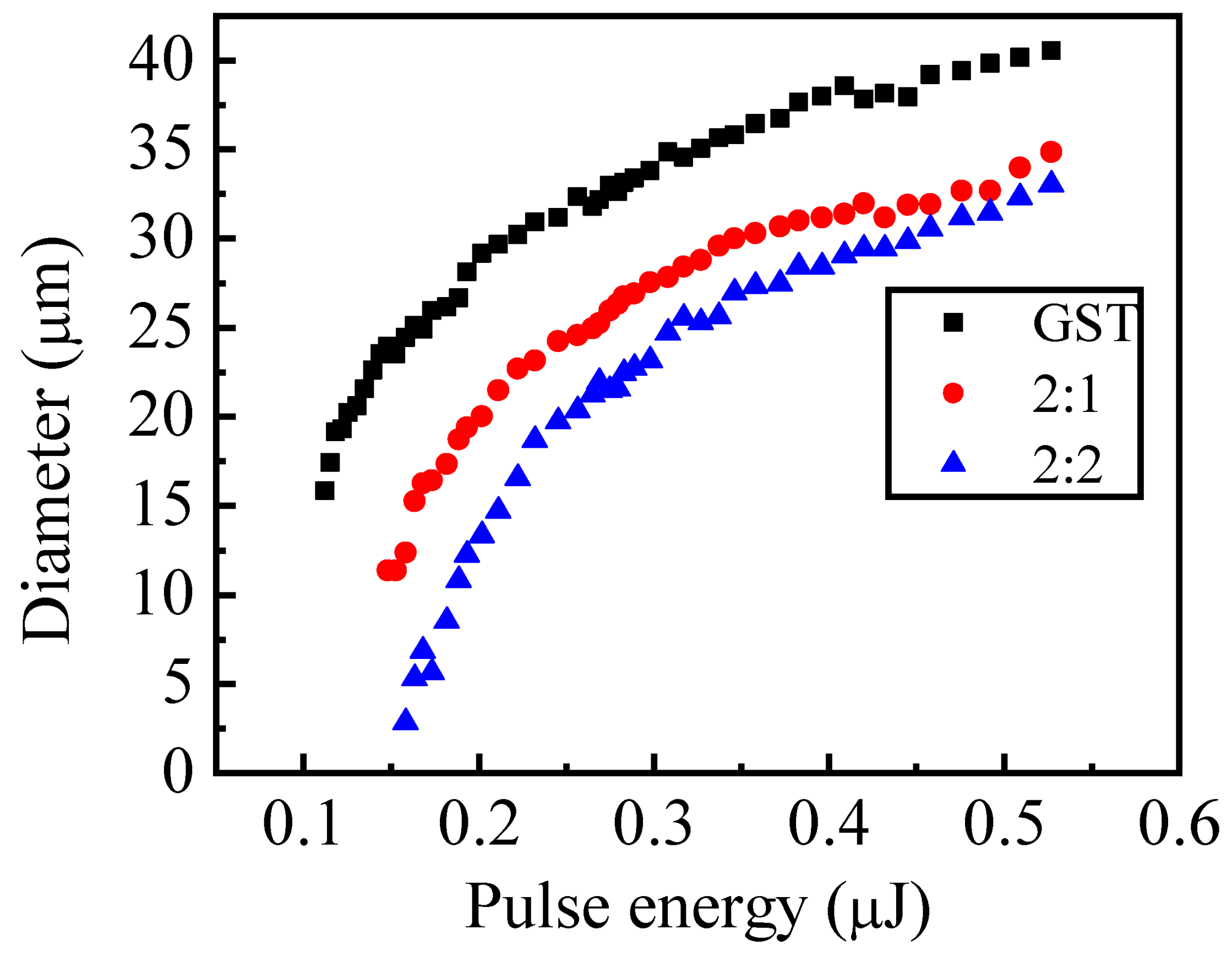
3.3. Threshold Evolution Analysis of Irradiation Regions
4. Conclusions
Author Contributions
Funding
Data Availability Statement
Conflicts of Interest
References
- Wuttig, M.; Yamada, N. Phase-change materials for rewriteable data storage. Nat. Mater. 2007, 6, 824–832. [Google Scholar] [CrossRef] [PubMed]
- Chua, E.K.; Shi, L.P.; Zhao, R.; Lim, K.G.; Chong, T.C.; Schlesinger, T.E.; Bain, J.A. Low resistance, high dynamic range reconfigurable phase change switch for radio frequency applications. Appl. Phys. Lett. 2010, 97, 183506. [Google Scholar] [CrossRef]
- Hosseini, P.; Wright, C.D.; Bhaskaran, H. An optoelectronic framework enabled by low-dimensional phase-change films. Nature 2014, 511, 206–211. [Google Scholar] [CrossRef]
- Hu, J.; Tarasov, V.; Agarwal, A.; Kimerling, L.; Carlie, N.; Petit, L.; Richardson, K. Fabrication and testing of planar chalcogenide waveguide integrated microfluidic sensor. Opt. Express 2007, 15, 2307–2314. [Google Scholar] [CrossRef]
- Guo, T.; Song, S.; Li, L.; Ji, X.; Li, C.; Xu, C.; Shen, L.; Xue, Y.; Liu, B.; Song, Z.; et al. The ultrafast phase-change memory with high-thermal stability based on SiC-doped antimony. Scr. Mater. 2017, 129, 56–60. [Google Scholar] [CrossRef]
- Lankhorst, M.H.R.; Ketelaars, B.W.S.M.M.; Wolters, R.A. Low-cost and nanoscale non-volatile memory concept for future silicon chips. Nat. Mater. 2005, 4, 347–352. [Google Scholar] [CrossRef] [PubMed]
- Pirovano, A.; Lacaita, A.L.; Benvenuti, A.; Pellizzer, F.; Hudgens, S.; Bez, R. Scaling analysis of phase-change memory technology. In Proceedings of the IEEE International Electron Devices Meeting 2003, Washington, DC, USA, 8–10 December 2003; pp. 29.6.1–29.6.4. [Google Scholar]
- Lai, S. Current status of the phase change memory and its future. In Proceedings of the IEEE International Electron Devices Meeting 2003 IEEE, Washington, DC, USA, 8–10 December 2003; pp. 10.1.1–10.1.4. [Google Scholar]
- Mao, Y.; Chen, Y.; Zhang, Q.; Wang, R.; Shen, X. Improvement of thermal stability and phase change behavior of Ge2Sb2Te5 thin films by Calcium doping. J. Non-Crystalline Solids 2020, 549, 120338. [Google Scholar] [CrossRef]
- Zhang, W.; Mazzarello, R.; Wuttig, M.; Ma, E. Designing crystallization in phase-change materials for universal memory and neuro-inspired computing. Nat. Rev. Mater. 2019, 4, 150–168. [Google Scholar] [CrossRef]
- Li, W.; Liu, F.; Zhang, Y.; Han, G.; Han, W.; Sun, N. Crystallization accompanied by local distortion behavior of Sn-doped amorphous Ge2Sb2Te5 induced by a picosecond pulsed laser. J. Non-Crystalline Solids 2019, 516, 99–105. [Google Scholar] [CrossRef]
- Kim, Y.; Jeong, K.; Cho, M.-H.; Hwang, U.; Jeong, H.S.; Kim, K. Changes in the electronic structures and optical band gap of Ge2Sb2Te5 and N-doped Ge2Sb2Te5 during phase transition. Appl. Phys. Lett. 2007, 90, 171920. [Google Scholar] [CrossRef]
- Guo, P.; Burrow, J.A.; Sevison, G.A.; Sood, A.; Asheghi, M.; Hendrickson, J.R.; Goodson, K.E.; Agha, I.; Sarangan, A. Improving the performance of Ge2Sb2Te5 materials via nickel doping: Towards RF-compatible phase-change devices. Appl. Phys. Lett. 2018, 113, 171903. [Google Scholar] [CrossRef]
- Wang, G.; Shen, X.; Lu, Y.; Dai, S.; Nie, Q.; Xu, T. Understanding the role of Zn in improving the phase change behaviors of Sb2Te3 films. Thin Solid Films 2015, 585, 57–65. [Google Scholar] [CrossRef]
- Fu, J.; Shen, X.; Nie, Q.; Wang, G.; Wu, L.; Dai, S.; Xu, T.; Wang, R. Crystallization characteristics of Mg-doped Ge2Sb2Te5 films for phase change memory applications. Appl. Surf. Sci. 2013, 264, 269–272. [Google Scholar] [CrossRef]
- Park, S.-J.; Kim, I.-S.; Kim, S.-K.; Yoon, S.-M.; Yu, B.-G.; Choi, S.-Y. Phase transition characteristics and device performance of Si-doped Ge2Sb2Te5. Semicond. Sci. Technol. 2008, 23, 105006. [Google Scholar] [CrossRef]
- Zhou, X.; Xia, M.; Rao, F.; Wu, L.; Li, X.; Song, Z.; Feng, S.; Sun, H. Understanding phase-change behaviors of carbon-doped Ge2Sb2Te5 for phase-change memory application. ACS Appl. Mater. Interfaces 2014, 6, 14207–14214. [Google Scholar] [CrossRef]
- Yao, D.; Zhou, X.; Wu, L.; Song, Z.; Cheng, L.; Rao, F.; Liu, B.; Feng, S. Investigation on nitrogen-doped Ge2Sb2Te5 material for phase-change memory application. Solid-State Electron. 2013, 79, 138–141. [Google Scholar] [CrossRef]
- Rao, F.; Ding, K.; Zhou, Y.; Zheng, Y.; Xia, M.; Lv, S.; Song, Z.; Feng, S.; Ronneberger, I.; Mazzarello, R.; et al. Reducing the stochasticity of crystal nucleation to enable subnanosecond memory writing. Science 2017, 358, 1423–1427. [Google Scholar] [CrossRef]
- Lu, H.; Thelander, E.; Gerlach, J.W.; Decker, U.; Zhu, B.; Rauschenbach, B. Single Pulse Laser-Induced Phase Transitions of PLD-Deposited Ge2Sb2Te5 Films. Adv. Funct. Mater. 2013, 23, 3621–3627. [Google Scholar] [CrossRef]
- Loke, D.; Lee, T.H.; Wang, W.J.; Shi, L.P.; Zhao, R.; Yeo, Y.C.; Chong, T.C.; Elliott, S.R. Breaking the Speed Limits of Phase-Change Memory. Science 2012, 336, 1566–1569. [Google Scholar] [CrossRef]
- Wang, Y.H.; Liu, F.R.; Li, W.Q.; Fan, T.; Yang, J.F.; Wang, Z.M.; Liu, F.; Sun, N.X. Study of non-equilibrium thermal transport in Ge2Sb2Te5 thin films under ultrafast laser excitation using a photo-excited carrier integrated semiconductor model. J. Appl. Phys. 2017, 122, 043104. [Google Scholar] [CrossRef]
- Wei, T.; Wang, Q.; Song, S.; Song, Z.; Liu, B. Reversible phase-change characteristics and structural origin in Cr doped Ge2Sb2Te5 thin films. Thin Solid Films 2020, 716, 138434. [Google Scholar] [CrossRef]
- Wang, Y.H.; Liu, F.R. Investigation of the evolution of free carriers during femtosecond laser-induced ultrafast amorphization in nitrogen doped Ge2Sb2Te5 films. J. Phys. Conf. Ser. 2020, 1676, 012113. [Google Scholar] [CrossRef]
- Wu, H.; Han, W.; Zhang, X. Ultrafast Dynamics of Different Phase States Ge2Sb2Te5 Film Induced by a Femtosecond Laser Pulse Irradiation. Materials 2022, 15, 6760. [Google Scholar] [CrossRef]
- Pan, C.; Jiang, L.; Sun, J.; Wang, Q.; Wang, F.; Wang, K.; Lu, Y.; Wang, Y.; Qu, L.; Cui, T. Ultrafast optical response and ablation mechanisms of molybdenum disulfide under intense femtosecond laser irradiation. Light. Sci. Appl. 2020, 9, 80. [Google Scholar] [CrossRef]
- Wei, T.; Wei, J.; Zhang, K.; Zhao, H.; Zhang, L. Rayscale image recording on Ge2Sb2Te5 thin films through laser-induced structural evolution. Sci. Rep. 2017, 7, 42712. [Google Scholar] [CrossRef]
- Fu, J.; Shen, X.; Xu, Y.; Wang, G.; Nie, Q.; Lin, C.; Dai, S.; Xu, T.; Wang, R. Structural evolution of Ge2Sb2Te5 films under the 488nm laser irradiation. Mater. Lett. 2012, 88, 148–151. [Google Scholar] [CrossRef]
- Kim, S.; Park, J.; Jung, S.; Lee, W.; Woo, J.; Cho, C.; Siddik, M.; Shin, J.; Park, S.; Lee, B.H.; et al. Excellent resistive switching in nitrogen-doped Ge2Sb2Te5 devices for field-programmable gate array configurations. Appl. Phys. Lett. 2011, 99, 192110. [Google Scholar] [CrossRef]
- Zhou, X.; Du, Y.; Behera, J.K.; Wu, L.; Song, Z.; Simpson, R.E. Oxygen tuned local structure and phase-change performance of germanium telluride. ACS Appl. Mater. Interfaces 2016, 8, 20185–20191. [Google Scholar] [CrossRef]
- Du, J.; Mu, Z.; Li, L.; Li, L. A Raman study on nanosecond-laser-induced multi-level switching of Ge2Sb2Te5 thin films. Opt. Laser Technol. 2021, 144, 107393. [Google Scholar] [CrossRef]
- Han, Z.H.; Han, W.; Liu, F.; Han, Z.; Yuan, Y.; Cheng, Z. Ultrafast temporal-spatial dynamics of amorphous-to-crystalline phase transition in Ge2Sb2Te5 thin film triggered by multiple femtosecond laser pulses irradiation. Nanotechnology 2019, 31, 115706. [Google Scholar] [CrossRef]
- Xu, Z.; Chen, C.; Wang, Z.; Wu, K.; Chong, H.; Ye, H. Optical constants acquisition and phase change properties of Ge2Sb2Te5 thin films based on spectroscopy. RSC Adv. 2018, 8, 21040–21046. [Google Scholar] [CrossRef]
- Zhou, G.-F. Materials aspects in phase change optical recording. Mater. Sci. Eng. A 2001, 304-306, 73–80. [Google Scholar] [CrossRef]
- Li, X.-B.; Liu, X.Q.; Han, D.; Zhang, Z.; Han, X.D.; Sun, H.-B.; Zhang, S.B. Role of Electronic Excitation in the Amorphization of Ge-Sb-Te Alloys. Phys. Rev. Lett. 2011, 107, 015501. [Google Scholar] [CrossRef]
- Friedrich, I.; Weidenhof, V.; Lenk, S.; Wuttig, M. Morphology and structure of laser-modified Ge2Sb2Te5 films studied by transmission electron microscopy. Thin Solid Films 2001, 389, 239–244. [Google Scholar] [CrossRef]
- Bonse, J.; Rudolph, P.; Krüger, J.; Baudach, S.; Kautek, W. Femtosecond pulse laser processing of TiN on silicon. Appl. Surf. Sci. 2000, 154–155, 659–663. [Google Scholar] [CrossRef]


Publisher’s Note: MDPI stays neutral with regard to jurisdictional claims in published maps and institutional affiliations. |
© 2022 by the authors. Licensee MDPI, Basel, Switzerland. This article is an open access article distributed under the terms and conditions of the Creative Commons Attribution (CC BY) license (https://creativecommons.org/licenses/by/4.0/).
Share and Cite
Wu, H.; Zhang, X.; Han, W. Ultrafast Temporal-Spatial Dynamics of Phase Transition in N-Doped Ge2Sb2Te5 Film Induced by Femtosecond Laser Pulse Irradiation. Micromachines 2022, 13, 2168. https://doi.org/10.3390/mi13122168
Wu H, Zhang X, Han W. Ultrafast Temporal-Spatial Dynamics of Phase Transition in N-Doped Ge2Sb2Te5 Film Induced by Femtosecond Laser Pulse Irradiation. Micromachines. 2022; 13(12):2168. https://doi.org/10.3390/mi13122168
Chicago/Turabian StyleWu, Hao, Xiaobin Zhang, and Weina Han. 2022. "Ultrafast Temporal-Spatial Dynamics of Phase Transition in N-Doped Ge2Sb2Te5 Film Induced by Femtosecond Laser Pulse Irradiation" Micromachines 13, no. 12: 2168. https://doi.org/10.3390/mi13122168
APA StyleWu, H., Zhang, X., & Han, W. (2022). Ultrafast Temporal-Spatial Dynamics of Phase Transition in N-Doped Ge2Sb2Te5 Film Induced by Femtosecond Laser Pulse Irradiation. Micromachines, 13(12), 2168. https://doi.org/10.3390/mi13122168