Abstract
Amorphous InGaZnO thin film transistors (a-IGZO TFTs) with double-stacked channel layers (DSCL) were quite fit for ultraviolet (UV) light detection, where the best DSCL was prepared by the depositions of oxygen-rich (OR) IGZO followed by the oxygen-deficient (OD) IGZO films. We investigated the influences of oxygen partial pressure (PO) for DSCL-TFTs on their sensing abilities by experiments as well as Technology Computer Aided Design (TCAD) simulations. With the increase in PO values for the DSCL depositions, the sensing parameters, including photogenerated current (Iphoto), sensitivity (S), responsivity (R), and detectivity (D*) of the corresponding TFTs, apparently degraded. Compared with PO variations for the OR-IGZO films, those for the OD-IGZO depositions more strongly influenced the sensing performances of the DSCL-TFT UV light detectors. The TCAD simulations showed that the variations of the electron concentrations (or oxygen vacancy (VO) density) with PO values under UV light illuminations might account for these experimental results. Finally, some design guidelines for DSCL-TFT UV light detectors were proposed, which might benefit the potential applications of these novel semiconductor devices.
1. Introduction
Ultraviolet (UV) light detectors have been extensively investigated in recent years due to their wide applications in flame detection, health motoring, environmental surveillance, and optical communication [1,2,3]. Amorphous oxide semiconductors (AOSs) are interesting materials for UV light detection because of their high transparency and wide band gap (Eg > 3 eV) [4,5,6]. Amorphous InGaZnO thin film transistors (a-IGZO TFTs) have especially attracted much attention as UV light detectors because of their great responsivity, small dark current, low manufacturing temperature, good uniformity, and outstanding electrical stability after bending [5,6,7,8,9,10]. In order to achieve higher UV light detectivity of a-IGZO TFTs, the researchers have reported several device improving methods, including choosing high-k gate dielectric materials, adding photosensitive absorption layers, adopting high work-function-difference capping layers, etc. [11,12,13]; on the other side, the optimization of processing conditions, e.g., using plasma enhanced atomic layer deposition (PEALD), adjusting oxygen partial pressure (PO) during preparations, etc., also seemed effective to make a-IGZO TFTs more sensitive to UV light illuminations [14,15,16,17].
Recently, we proposed to use double-stacked channel layers (DSCL) to increase the detecting abilities of a-IGZO TFT UV sensors, resulting in a good sensitivity of 28.6 dB when they were illuminated by 370 nm UV light [18]. In contrast to the optimized DSCL structure for general-purpose TFT devices [19], the best DSCL deposition consequence of oxygen-rich (OR) IGZO followed by oxygen-deficient (OD) IGZO was proven for UV light detection [18]. However, the detailed design methods as well as the related physical essence are still unknown for a-IGZO TFTs with DSCL (DSCL-TFTs) UV light detectors.
In this study, the UV light response properties of the DSCL-TFTs using various PO were comparatively investigated, with the related physical mechanisms demonstrated through experiments as well as Technology Computer Aided Design (TCAD) simulations. It was found that the UV light photogenerated current (Iphoto), sensitivity (S), responsivity (R), and detectivity (D*) of the DSCL-TFTs increased when PO for the DSCL depositions became smaller. In addition, the back channel (OD-IGZO) was more sensitive to PO variation than the front channel (OR-IGZO) under UV light illuminations. X-ray photoemission spectroscopy (XPS) and ultraviolet-visible spectrophotometer (UVS) measurements were employed to ascertain the variations of the defect density and light absorption with PO for a-IGZO depositions. Finally, a qualitative model was proposed and elaborated to explain these experimental data through TCAD simulations.
2. Materials and Methods
Five samples of DSCL-TFTs (Device 1–5) were prepared on the p++ silicon wafers (gate electrodes) with 500 nm-thick SiO2 (gate insulators), with the schematic cross-section shown in the inset of Figure 1a. Among them, Device 2 was used as the reference sample. All the devices had the same structures but the processing conditions of their channel layers were different, as shown in Table 1. Both the OD-IGZO and OR-IGZO were deposited via magnetron sputtering, where the atomic ratio of the target was In: Ga: Zn = 1:1:1. After the DSCL depositions, the 200 nm-thick indium tin oxide (ITO) layers were prepared as source/drain (S/D) electrodes, followed by the 50 nm-thick SiO2 layers as passivation layers. Both the S/D electrodes and the passivation layers were also deposited by magnetron sputtering. Three shadow masks were used to pattern the DSCL, S/D electrodes, and passivation layers during sputtering, leading to the channel width/length of 1000 μm/275 μm, respectively. Finally, all the samples were annealed at 425 °C in N2 for 7200 s.
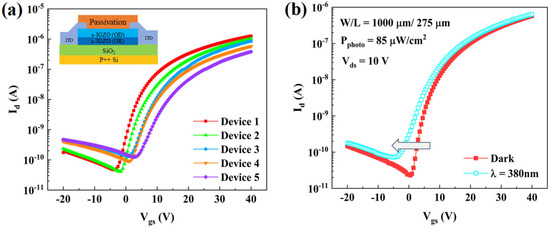
Figure 1.
(a) Transfer curves of the DSCL-TFTs in dark, with the inset denoting the schematic cross-section of the five samples; (b) transfer curve evolution of Device 1 under 380 nm UV light illumination for 600 s.

Table 1.
Oxygen partial pressure for the channel-layer depositions of the DSCL-TFTs (Unit: mPa).
The electrical properties of the DSCL-TFTs were measured at room temperature (RT) using a Keithley 2636 semiconductor parameter analyzer (Solon, OH, USA). The 380 nm UV light illumination was achieved by the combination of a 150 W Xenon lamp, a monochromator, and an optical fiber. The incident optical power density was measured by an optical power meter (Thorlabs, PM100A, Newton, NJ, USA) with a Si photodiode sensor (Thorlabs, S120VC, Newton, NJ, USA), which was confirmed as 0.085 mW/cm2. The transmittance and the chemical bonding states of a-IGZO films were measured by a UV-visible spectrophotometer (EVOLUTION 300, Waltham, MA, USA) and an XPS analyzer (AXIS Ultra DLD, Manchester, UK), respectively. In order to thoroughly clean the sample surfaces, 10 nm-depth Ar-ion etching treatments were employed before recording the XPS spectra. Victory Device, one of the most popular TCAD tools from Silvaco, Inc., (Santa Clara, CA, USA) was used to investigate the physical essence relating the experimental results reported in this study [20].
3. Results and Discussion
Figure 1a shows the transfer characteristics of the five samples. One may notice that the transfer curves of the DSCL-TFTs shifted positively with PO (for the channel-layer depositions) increasing which is consistent with other reports [21]. Interestingly, these curves were quite sensitive to the UV light illuminations. As shown in Figure 1b, the transfer curve of Device 1 apparently shifted in the negative direction when it was illuminated by the 380 nm UV light for 600 s. However, this sensitivity to the UV light illumination was different for the five samples, implying that the PO values for the DSCL depositions evidently influenced the defect density in a-IGZO under UV light illuminations.
In order to quantitatively study the sensing properties of the DSCL-TFTs, we defined some useful terms, i.e., net photogenerated current (Iphoto), sensitivity (S), responsivity (R), and detectivity (D*) [4,18]. Iphoto was defined as follows:
where Iilluminated is the total photo current under illumination and Idark is the dark current. In this study, Idark was fixed as 10−10 A for all the measurements and Iilluminated was obtained under the same gate voltage corresponding to Idark.
Sensitivity (S), the ratio of the net photogenerated current and the dark current of the photodetectors, was defined as follows:
Responsivity (R), the ratio of the net photogenerated current and the incident light power of the photodetectors, was defined as follows:
where Plight is the incident light power.
Detectivity (D*), a figure about the minimum detection of photodetectors, which was considered as the normalization of responsivity [16], was defined as follows:
where e is elementary charge and Jdark is the dark current density.
Figure 2a,b demonstrates the dependence of Iphoto, S, R, and D* on PO for the OD-IGZO depositions. Here, the PO values for OD-IGZO increased from 0 mPa to 14 mPa, while PO for OR-IGZO was fixed at 21 mPa. On the other hand, Figure 2c,d shows the influence of PO for the OR-IGZO depositions on Iphoto, S, R, and D*. Here, the PO values for OR-IGZO increased from 21 mPa to 56 mPa, while PO for OD-IGZO was fixed at 7 mPa. Obviously, all these parameters, including Iphoto, S, R, and D*, decreased with PO increasing. In addition, for the purpose of analyzing the UV light sensing degradation of the DSCL-TFTs with the increase in PO values, the variation ratio ΔIphoto/ΔPO was defined in this study (see Table 2). For the case of the PO variation for OD-IGZO, ΔIphoto/ΔPO was −7.5 × 10⁻¹¹ A·mPa−1. However, when the PO value for OR-IGZO changed, ΔIphoto/ΔPO became −1.9 × 10⁻¹¹ A·mPa−1. Similarly, when PO for OD-IGZO increased, ΔS/ΔPO, ΔR/ΔPO, and ΔD*/ΔPO were −1.9 dB·mPa−1, −3.2 × 10⁻⁴ A·W−1·mPa−1, and −2.2 × 10⁹ Jones·mPa−1, respectively. However, when PO for OR-IGZO increased, ΔS/ΔPO, ΔR/ΔPO, and ΔD*/ΔPO were −0.8 dB·mPa−1, −8.2 × 10⁻⁵ A·W−1·mPa−1, and −5.6 × 10⁸ Jones·mPa−1, respectively. We may draw a conclusion that the UV light response properties of the DSCL-TFTs were more sensitive to PO variations for the back channel (OD-IGZO) than those for the front channel (OR-IGZO). These results are consistent with a recent publication, which indicated that the oxygen vacancies (VO) located at the back channel of the a-IGZO layer played an important role in UV light response [22]. This conclusion might lead to some new approaches to improving the DSCL-TFT UV light detectors by the modulation of PO valves.
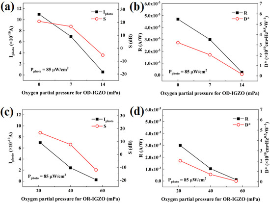
Figure 2.
Dependence of the oxygen partial pressures for OD-IGZO on (a) Iphoto/S and (b) R/D* of the DSCL-TFTs; dependence of the oxygen partial pressures for OR-IGZO on (c) Iphoto/S and (d) R/D* of the DSCL-TFTs.
Table 2.
Variations of the UV light detecting performances with ΔPO for OD-IGZO and OR-IGZO.
To analyze the physical essence relating the abovementioned experimental results, we used a UV-visible spectrophotometer and an XPS analyzer to characterize the differences between the material properties of OD-IGZO and OR-IGZO. Figure 3 illustrates the transmittance spectra of OD-IGZO and OR-IGZO films, the corresponding Tauc plots, and linear fitting lines, which are shown in the insets. After obtaining the adsorption spectra from the transmittance spectra, we derived the optical energy band gaps by Tauc law using the following equation [19]:
where α is the absorption coefficient, h is the Planck constant, hυ represents the photon energy, and A is a constant related to UV light adsorption. The value of Eg was determined by the intersection point of the linear fitting line and the x-axis. The overall transmittances of all the a-IGZO films were larger than 90% in the visible light region, though they quickly dropped when the light wavelength decreased below 400 nm, confirming the good UV light adsorption of a-IGZO films. As shown in Figure 3, both OD-IGZO and OR-IGZO exhibited almost the same optical bandgap values, i.e., around 3.7 eV. This suggests that PO for a-IGZO depositions hardly influenced the UV light absorption of a-IGZO films in this study.
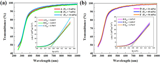
Figure 3.
Transmittance spectra of (a) OD-IGZO and (b) OR-IGZO films; the insets show the fitting curves and the optical band gaps of OD-IGZO and OR-IGZO films, respectively. Here, the six samples (A, B, C, D, E, and F) were sputtered at PO = 0, 7, 14, 21, 40, and 56 mPa, respectively.
Figure 4 depicts the XPS spectra of O1s signals in the six a-IGZO films (samples A, B, C, D, E, and F) prepared at various PO values (0, 7, 14, 21, 40, and 56 mPa, respectively), corresponding to the channel-layer deposition conditions for the DSCL-TFTs shown in Figure 1. All the O1s spectra were calibrated by using the C1s (284.8 eV) as the reference [23,24,25,26], where the O1s peak was deconvoluted into three Gaussian fitting sub-peaks that approximately centered at 530.3 eV (OI), 531.0 eV (OII), and 532.2 eV (OIII), respectively. The low binding energy OI peak could be attributed to the oxygen bonds with metal, the high binding energy OIII peak might be related to the hydrated oxides defects, and the middle binding energy OII peak was associated with oxygen vacancies (VO) [26]. In order to characterize the variations of VO with the PO values for IGZO deposition, the peak area ratio of the OII over the total area of O1s peak (OTotal = OI + OII + OIII) was calculated. One may notice that the area ratio OII/OTotal decreased from 20.7% to 10.8% when PO increased from 0 mPa to 56 mPa. These results proved that the VO density of the a-IGZO layer evidently decreased with PO increasing during its deposition.
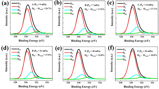
Figure 4.
The XPS measurement and analysis results of the six a-IGZO films. Here, samples A (a), B (b), C (c), D (d), E (e), and F (f) were deposited at the oxygen partial pressure of 0, 7, 14, 21, 40, and 56 mPa, respectively.
So far, three important results have been obtained from the aforementioned experiments: (1) The UV light response properties of the DSCL-TFTs evidently depended on the PO value for the channel layer depositions; (2) The PO variation for OD-IGZO at the top side of DSCL showed stronger influences on DSCL-TFT UV detectors than that for OR-IGZO at the bottom side of DSCL; (3) PO hardly influenced the UV light absorption of a-IGZO films but evidently changed the defect density, especially the Vo density. To ascertain the related physical mechanisms, we employed TCAD simulations and analysis on the DSCL-TFTs illuminated by UV lights. Exponential and Gaussian functions were used to model the band tail states and deep states in a-IGZO films, respectively. Specifically, the donor-like tail states (gTD), the acceptor-like tail states (gTA), the donor-like deep states (gGD), and the acceptor-like deep states (gGA) were defined as Equations (6)–(9) [20]. Here, Ec and Ev is the conduction band edge energy and the valence band edge energy, respectively. The exact meanings of the corresponding parameters are all listed in Table 3.
Table 3.
Typical simulation parameters for a-IGZO films in DSCL-TFTs.
As shown in Table 3, n(VO) is the initial Vo concentration and n(VO2+) represents the initial secondary ionized VO concentration. For the simulations, there were two reactions to describe the ionization process in a-IGZO [20]:
Here, and represent neutral oxygen vacancy and secondary ionized oxygen vacancy, respectively. Reaction (10) indicates that n(VO2+) should be affected by n(VO), which is related to PO for a-IGZO deposition. Accordingly, n(VO2+) is indirectly influenced by the PO value. It is generally believed that NGD is mainly associated with the VO density [19,21]. Therefore, n(VO), n(VO2+), and NGD are all connected to the PO values for a-IGZO depositions.
Figure 5a shows the fitting results between the simulation data and the experimental transfer curve. With the typical parameters listed in Table 3 and the device built in the inset of Figure 5a, the simulated transfer curve of the DSCL-TFTs agreed well with the experimental data, suggesting that our TCAD model could be used to investigate the physical essence relating the experiments employed in this study. The distribution of the electron concentration (ne) in DSCL is exhibited in Figure 5b when Vgs = 0 V. Figure 5b shows the detailed simulation results about the area highlighted by a red arrow in the inset of Figure 5a. One may observe that the electron concentration gradually decreased from the back channel to the front channel, where the ne values at the back channel and the front channel were 1 × 1014 cm−3 and 1 × 1013 cm−3, respectively. This was consistent with the XPS characterization results shown in Figure 4.
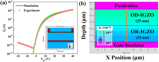
Figure 5.
(a) The typical transfer curves of the DSCL-TFTs from the simulation results and the experimental data, with the inset being the simulated device structure; (b) the simulated electron concentration distribution in the reference device.
After the DSCL-TFTs were illuminated by the 380 nm UV light for 600 s, the electron concentration ne increased to ne′. The variation of the electron concentration (Δne = ne′ − ne) could microscopically denote the UV light sensing abilities of the DSCL-TFTs. Apparently, the larger the Δne value, the more sensitive the sample. As shown in Figure 6, Δne of the reference sample gradually decreased from the back channel to the front channel. The simulation studies exhibited that Δne apparently decreased by increasing PO either for OD-IGZO (as shown in Figure 6a) or for OR-IGZO (as shown in Figure 6b). This result explained the experimental results shown in Figure 2, i.e., the UV light sensing abilities of the DSCL-TFTs became worse with PO increasing. On the other side, the PO modulation effects from the OD-IGZO and OR-IGZO were different. From the aforementioned experiments, the PO variation for OD-IGZO deposition showed stronger influence than that for OR-IGZO. To more deeply explore this difference, we calculated the total Δne by summing all the data points shown in Figure 6a,b. As shown in Table 4, the increase in PO for OD-IGZO showed stronger influences on the total Δne than that for OR-IGZO, which is also consistent with the measurement results shown in Figure 2. It is well known that the electron concentration closely relates oxygen vacancies and the other defects in a-IGZO [27,28], so the simulation results shown in Figure 6 also reflected how the defects (especially VO) changed with PO and UV light illuminations. Therefore, for DSCL-TFT UV light detectors, the defects in OD-IGZO (especially the VO density) were more easily modulated by PO than those in OR-IGZO.
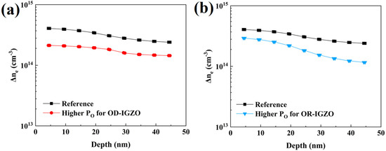
Figure 6.
The simulated Δne distributions in DSCL with varying depth for the cases of (a) increasing PO for OD-IGZO and (b) increasing PO for OR-IGZO.
Table 4.
Total net photogenerated electron concentration of the DSCL-TFTs.
According to all the experimental data and simulation results, we made a deeper discussion on the PO effect for DSCL-TFT UV light response. From the UVS characterization results shown in Figure 3, we could assume that band-to-band electron excitation would be nearly the same for all the devices in this study. On the one hand, the net photogenerated electron concentration (Δne) decreased with PO for DSCL increasing and the photogenerated VO2+ were believed to play an important role in UV light sensing [22,28]. Therefore, we could suppose that the PO increase during the DSCL depositions might reduce the concentration of photogenerated VO2+ and result in smaller Δne in the channel layers. There are two main photogenerated VO creation mechanisms under the UV light illuminations, which could be formed by using the energy released from electron-hole recombination or photogenerated owing to the high energy photons [22]. Therefore, the concentration of photogenerated VO2+ might decrease when PO for a-IGZO depositions increased; this might be induced by lower photoionization of VO to VO2+ rather than lower VO creation under the illumination, because the photogenerated VO might hardly be affected by the PO value for a-IGZO. In other words, when the PO value for a-IGZO deposition increased, VO2+ from the photoionization of VO decreased, resulting in a decrease in Δne and thus less UV light sensing for the DSCL-TFTs.
Finally, we may reach some design guidelines for DSCL-TFT UV detectors: (1) The DSCL consisting of an OD-IGZO (top side) and an OR-IGZO (bottom side) is the best choice for UV light detection; (2) For the deposition of DSCL, lower oxygen partial pressures are preferred; (3) To modulate the UV light sensing abilities of DSCL-TFTs, the OD-IGZO, rather than OR-IGZO, is more sensitive to variations in PO values.
4. Conclusions
The influences of oxygen partial pressures for DSCL-TFTs on their UV light sensing abilities were investigated by both experimental studies and TCAD simulations. With the increase in PO values for the DSCL depositions, the sensing parameters, including Iphoto, S, R, and D* of the corresponding TFTs, apparently became worse. Compared with the PO variations for the OR-IGZO films, those for the OD-IGZO depositions showed stronger influences on the sensing performances of the DSCL-TFT UV light detectors. The TCAD simulations indicated that the variations of the electron concentrations (or the VO density) with PO values under UV light illuminations should be responsible for the aforementioned experimental results. Some design guidelines for DSCL-TFT UV light detectors were finally proposed for the potential applications of these novel semiconductor devices.
Author Contributions
Conceptualization, Z.F. and C.D.; data curation, Z.F. and A.S.; software, Z.F., A.S., Y.X. and C.D.; Writing–original draft preparation, Z.F., A.S., Y.X. and C.D. All authors have read and agreed to the published version of the manuscript.
Funding
This work was supported by the Key Research Project of Jiangxi Province (Grant No. 20194ABC28005).
Data Availability Statement
The data presented in this study are available on request from the corresponding author.
Acknowledgments
This work was supported by the Key Research Project of Jiangxi Province (Grant No. 20194ABC28005). The authors thank the University Project from Silvaco, Inc.
Conflicts of Interest
The authors declare no conflict of interest.
References
- Zhou, H.; Li, L.; Chen, H.; Guo, Z.; Jiao, S.; Sun, W. Realization of a fast-response flexible ultraviolet photodetector employing a metal-semiconductor-metal structure InGaZnO photodiode. R. Soc. Chem. Adv. 2015, 5, 87993–87997. [Google Scholar] [CrossRef]
- Park, J.; Lee, H. Improvement of the Performance and Stability of Oxide Semiconductor Thin-Film Transistors Using Double-Stacked Active Layers. IEEE Electron Device Lett. 2012, 33, 818–820. [Google Scholar] [CrossRef]
- Ferhati, H.; Djeffal, F. Giant responsivity of a new InGaZnO Ultraviolet thin-film phototransistor based on combined dual gate engineering and surface decorated Ag nanoparticles aspects. Sens. Actuators A Phys. 2020, 318, 112523. [Google Scholar] [CrossRef]
- Singh, A.; Chourasia, N.; Pal, B.; Pandey, A.; Chakrabarti, P. A Proposed All ZnO Based Thin Film Transistor For UV-B Detection. IEEE Photonics Technol. Lett. 2020, 32, 1548–1551. [Google Scholar] [CrossRef]
- Nomura, K.; Ohta, H.; Takagi, A.; Kamiya, T.; Hirano, M.; Hosono, H. Room-temperature fabrication of transparent flexible thin-film transistors using amorphous oxide semiconductors. Nature 2004, 432, 488–492. [Google Scholar] [CrossRef]
- Kamiya, T.; Nomura, K.; Hosono, H. Present status of amorphous In-Ga-Zn-O thin-film transistors. Sci. Technol. Adv. Mater. 2010, 11, 044305. [Google Scholar] [CrossRef] [PubMed]
- Jeong, J.; Jeong, J.; Choi, J.; Im, J.; Kim, S.; Yang, H.; Kang, K.; Kim, K.; Ahn, T.; Chung, H.; et al. 3.1: Distinguished Paper: 12.1-Inch WXGA AMOLED display driven by indium-gallium-zinc oxide TFTs array. SID Symp. Dig. Tech. Pap. 2008, 39, 1–4. [Google Scholar] [CrossRef]
- Yabuta, H.; Sano, M.; Abe, K.; Aiba, T.; Den, T.; Kumomi, H.; Nomura, K.; Kamiya, T.; Hosono, H. High-mobility thin-film transistor with amorphous InGaZnO4 channel fabricated by room temperature rf-magnetron sputtering. Appl. Phys. Lett. 2006, 89, 112123. [Google Scholar] [CrossRef]
- Chen, Y.; Chang, T.; Li, H.; Hsieh, T.; Chen, T.; Wu, C.; Chou, C.; Chung, W.; Chang, J.; Tai, Y. The suppressed negative bias illumination-induced instability in In-Ga-Zn-O thin film transistors with fringe field structure. Appl. Phys. Lett. 2012, 101, 223502. [Google Scholar] [CrossRef]
- Choi, S.; Kim, J.; Kang, H.; Ko, D.; Rhee, J.; Choi, S.J.; Kim, D.M.; Kim, D.H. Effect of Oxygen Content on Current Stress-Induced Instability in Bottom-Gate Amorphous InGaZnO Thin-Film Transistors. Materials 2019, 12, 3149–3159. [Google Scholar] [CrossRef]
- Lu, H.; Zhou, X.; Liang, T.; Zhang, L.; Zhang, S. Oxide TFTs with IMO and IGZO stacked active layers for UV detection. J. Electron Devices Soc. 2017, 5, 504–508. [Google Scholar] [CrossRef]
- Yu, J.; Javaid, K.; Liang, L.; Wu, W.; Liang, Y.; Song, A.; Zhang, H.; Shi, W.; Chang, T.; Cao, H. High-Performance visible-blind ultraviolet photodetector based on IGZO TFT coupled with p−n heterojunction. ACS Appl. Mater. Interfaces 2018, 10, 8102–8109. [Google Scholar] [CrossRef] [PubMed]
- Tak, Y.; Kim, D.; Kim, W.; Lee, J.; Kim, S.; Kim, J.; Kim, H. Boosting visible light absorption of metal-oxide-Based phototransistors via heterogeneous in-Ga-Zn-O and CH3NH3PbI3 films. ACS Appl. Mater. Interfaces 2018, 10, 12854–12861. [Google Scholar] [CrossRef]
- Chen, K.; Hsu, C.; Yu, H.; Peng, Y.; Yang, C.; Su, Y. The effect of oxygen vacancy concentration on Indium Gallium Oxide solar blind photodetector. IEEE Trans. Electron Devises 2018, 65, 1817–1822. [Google Scholar] [CrossRef]
- Jang, J.; Ko, D.; Choi, S.; Kang, H.; Kim, J.; Yu, H.; Ahn, G.; Jung, H.; Rhee, J.; Lee, H.; et al. Effects of structure and oxygen flow rate on the photo-response of amorphous IGZO-based photodetector devices. Solid State Electron. 2018, 140, 115–121. [Google Scholar] [CrossRef]
- Wang, X.; Shao, Y.; Wu, X.; Zhang, M.; Li, L.; Liu, W.; Zhang, D.; Ding, S. Light response behaviors of amorphous In-Ga-Zn-O thin-film transistors via in situ interfacial hydrogen doping modulation. RSC Adv. 2020, 10, 3572. [Google Scholar] [CrossRef] [PubMed]
- Chen, X.; He, G.; Liu, M.; Zhang, J.; Deng, B.; Wang, P.; Zhang, M.; Lv, J.; Sun, Z. Modulation of optical and electrical properties of sputtering-derived amorphous InGaZnO thin films by oxygen partial pressure. J. Alloys Compd. 2014, 615, 636–642. [Google Scholar] [CrossRef]
- Fan, Z.; Zhang, W.; Shen, A.; Dong, C. Ultraviolet Light Response of Amorphous Oxide Thin-Film Transistors with Double-Stacked Channel Layers. SID Symp. Dig. Tech. Pap. 2022, 53, 621–624. [Google Scholar] [CrossRef]
- Xie, H.; Wu, Q.; Xu, L.; Zhang, L.; Liu, G.; Dong, C. Nitrogen-doped amorphous oxide semiconductor thin film transistors with double-stacked channel layers. Appl. Surf. Sci. 2016, 387, 237–243. [Google Scholar] [CrossRef]
- Victory Device User’s Manual, Silvaco TCAD. 2019. Available online: https://www.silvaco.com/tcad.html (accessed on 2 November 2022).
- Xiao, X.; Deng, W.; Chi, S.; Shao, Y.; He, X.; Wang, L.; Zhang, S. Effect of O2 Flow Rate During Channel Layer Deposition on Negative Gate Bias Stress-Induced Vth Shift of a-IGZO TFTs. IEEE Trans. Electron Devices 2013, 60, 4159–4164. [Google Scholar] [CrossRef]
- Mativenga, M.; Haque, F.; Billah, M.; Um, J. Origin of light instability in amorphous IGZO thin-film transistors and its suppression. Sci. Rep. 2021, 11, 14618. [Google Scholar] [CrossRef] [PubMed]
- Xie, H.; Xu, J.; Liu, G.; Zhang, L.; Dong, C. Development and analysis of nitrogen-doped amorphous InGaZnO thin film transistors. Mater. Sci. Semicond. Process. 2017, 64, 1–5. [Google Scholar] [CrossRef]
- Zhang, W.; Fan, Z.; Shen, A.; Dong, C. Atmosphere Effect in Post-Annealing Treatments for Amorphous InGaZnO Thin-Film Transistors with SiOx Passivation Layers. Micromachines 2021, 12, 1551. [Google Scholar] [CrossRef] [PubMed]
- Cochran, E.; Park, D.; Kast, M.; Enman, L.; Perkins, C.; Mansergh, R.; Keszler, D.; Johnson, D.; Boettcher, S. Role of Combustion Chemistry in Low-Temperature Deposition of Metal Oxide Thin Films from Solution. Chem. Mater. 2017, 29, 9480–9488. [Google Scholar] [CrossRef]
- Sen, A.; Park, H.; Pujar, P.; Bala, A.; Cho, H.; Liu, N.; Gandla, S.; Kim, S. Probing the Efficacy of Large-Scale Nonporous IGZO for Visible-to-NIR Detection Capability: An Approach toward High-Performance Image Sensor Circuitry. ACS Nano 2022, 16, 9267–9277. [Google Scholar] [CrossRef]
- Ryu, B.; Noh, H.; Choi, E.; Chang, K. O-vacancy as the origin of negative bias illumination stress. Appl. Phys. Lett. 2010, 97, 022108. [Google Scholar] [CrossRef]
- Yang, G.; Park, J.; Choi, S.; Kim, C.; Kim, D.; Choi, S.-J.; Bae, J.-H.; Cho, I.; Kim, D.H. Total Subgap Range Density of States-Based Analysis of the Effect of Oxygen Flow Rate on the Bias Stress Instabilities in a-IGZO TFTs. IEEE Trans. Electron Devices 2022, 69, 166–173. [Google Scholar] [CrossRef]


Publisher’s Note: MDPI stays neutral with regard to jurisdictional claims in published maps and institutional affiliations. |
© 2022 by the authors. Licensee MDPI, Basel, Switzerland. This article is an open access article distributed under the terms and conditions of the Creative Commons Attribution (CC BY) license (https://creativecommons.org/licenses/by/4.0/).