Article

A 100 KS/s 8–10-Bit Resolution-Reconfigurable SAR ADC for Biosensor Applications †

1
University of Electronic Science and Technology of China, Zhongshan Institute, Zhongshan 528402, China
2
School of Microelectronics, South China University of Technology, Guangzhou 510640, China
*
Author to whom correspondence should be addressed.
This paper is an extended version of our paper published in the 2019 32nd IEEE International System-on-Chip Conference (SOCC) was held in Singapore, 3–6 September 2019.
Micromachines 2022, 13(11), 1909; https://doi.org/10.3390/mi13111909
Submission received: 15 September 2022 / Revised: 25 October 2022 / Accepted: 1 November 2022 / Published: 5 November 2022
(This article belongs to the Special Issue Frontiers in Biosensors)

Abstract

:
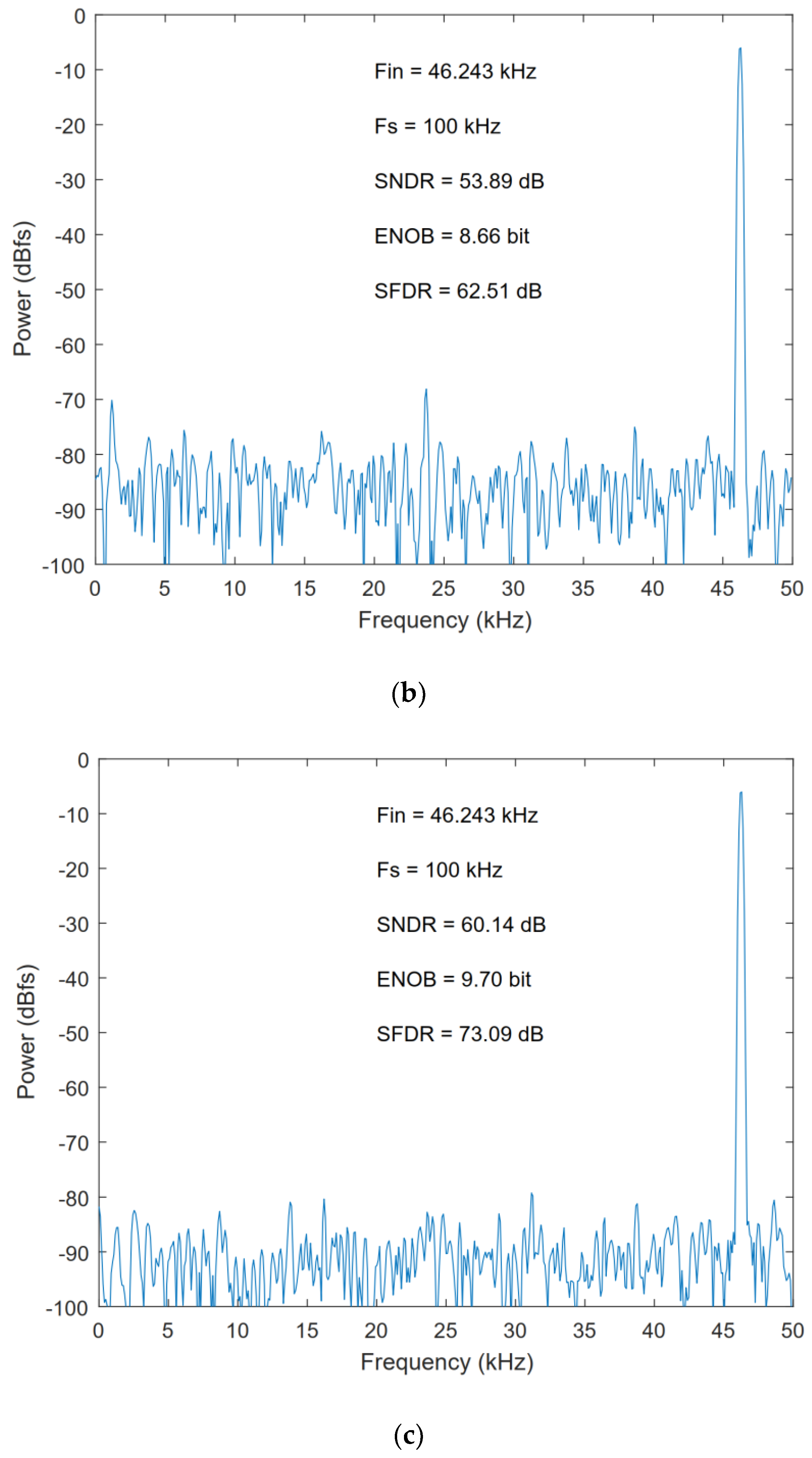
A DAC switching scheme that combines energy efficiency and resolution reconfigurability is proposed. Compared with the conventional switching scheme, the proposed scheme achieves 93.8%, 96.1%, and 97.3% switching energy saving in 8-bit, 9-bit, and 10-bit modes, respectively. Based on the proposed switching scheme, an 8–10-bit resolution-reconfigurable SAR ADC for biosensor applications is designed. The ADC consists of resolution-reconfigurable binary-weighted capacitive DAC, a two-stage full dynamic comparator, sampling switch, and the resolution-control SAR logic. Simulated in 180 nm CMOS process and 100 kS/s sampling rate, the ADC achieves the 46.80/53.89/60.14 dB signal-to-noise and distortion ratio (SNDR), the 55.22/62.51/73.09 dB spurious-free dynamic range (SFDR) and the 0.81/0.91/1.01 μW power consumption in 8/9/10-bit mode, respectively.

1. Introduction

In recent years, successive-approximation register (SAR) analogue-to-digital converters (ADCs) have been preferred for biosensor applications [1,2,3,4,5]. SAR ADC is based on a successive approximation algorithm, which is suitable for designing resolution-reconfigurable SAR ADCs [6,7,8]. Resolution-reconfigurable ADCs can choose the appropriate resolution according to the characteristics of the biomedical signal, thus reducing energy consumption. Recently, several energy-efficient DAC switching schemes have been developed to improve the power efficiency of DAC capacitor arrays [9,10,11]. Compared to a conventional switching scheme [12], capacitor splitting [9], set and down [10], and Vcm-based [11] reduce the switching energy by 37.4%, 81.3%, and 87.5%, respectively. However, their switching energy doubles as the number of bits increases by one. Taking the Vcm-based switching scheme as an example, the average switching energy of 8-bit, 9-bit and 10-bit is 42.2 C V r e f 2 , 84.8 C V r e f 2 and 170.2 C V r e f 2 , respectively.
In this paper, a DAC switching scheme that combines energy efficiency and resolution reconfigurability is proposed. The average switching energy of the proposed switching scheme for 8-bit, 9-bit, and 10-bit SAR ADCs is 21.2 C V r e f 2 , 26.5 C V r e f 2 , and 37.1 C V r e f 2 , which amounts to a reduction of 93.8%, 96.1% and 97.3% in the switching energy compared with a conventional switching scheme [9]. Based on the proposed switching scheme, a 100 KS/s 8–10-bit resolution-reconfigurable SAR ADC for biosensor applications is designed and simulated. In order to reduce the on-resistance of the sampling switch and reduce the sampling error, the sampling switch adopts a bootstrap switch circuit [13]. A two-stage full dynamic comparator is used to achieve low power consumption [14]. To improve the performance of SAR logic, a dynamic logic unit is used [15]. Based on the SAR logic, we design a resolution control circuit for bit control. When the SAR ADC is operating in 8-bit or 9-bit resolutions, in order to save power, two or one dynamic logic units need to be skipped, respectively. The frequency range of various biomedical signals are shown in Table 1. The 100KS/s sampling rate can meet these biomedical signal sensing applications.
This paper is organized as follows: Section 2 describes the ADC architecture and presents the techniques used to achieve resolution reconfigurability and low power; the simulated results and the comparison with the state of the art are provided in Section 3. The conclusion is drawn in Section 4.

2. Proposed SAR ADC Architecture

Figure 1 shows the architecture of the proposed 8–10-bit resolution-reconfigurable SAR ADC. It comprises a resolution-reconfigurable binary-weighted capacitive DAC, a two-stage full dynamic comparator, sampling switch, and the resolution-control SAR logic.

2.1. Proposed DAC Switching Scheme

The proposed DAC switching scheme is similar to a Vcm-based switching scheme [11]. However, the proposed DAC has replaced the dummy capacitor with the C-2C capacitors, which add one bit of accuracy, and adds some switches (S1 and S2) to adjust the resolution. As shown in Table 2, resolutions of ADC are adjusted by S1 and S2. In the 8-bit mode, S1 and S2 are always opened (except in the sampling phase). For the 9-bit mode, S1 will be closed in the 3rd comparison, with S2 remaining open. For the 10-bit mode, S1 will be closed in the 3rd comparison and S2 will be closed in the 4th comparison. A special reference switching method, which is shown in Table 3 and Table 4, is used for the references (RP2, RN2, RP3 and RN3) associated with switches S1 and S2. Table 3 shows the references of RP2 and RN2 for each phase in 9-bit and 10-bit modes. The references of RP2 and RN2 are determined by the results of the 1st comparison (D1) and the 2nd comparison (D2). Table 4 shows the references of RP3 and RN3 for each phase in 10-bit mode. RP3 and RN3 are determined by the results of the first comparison (D1) and the 3rd comparison (D3).
To explain the operation of the SAR ADC, the proposed switching scheme in the three modes is used as follows.

2.1.1. Proposed 8-Bit Mode Switching Scheme

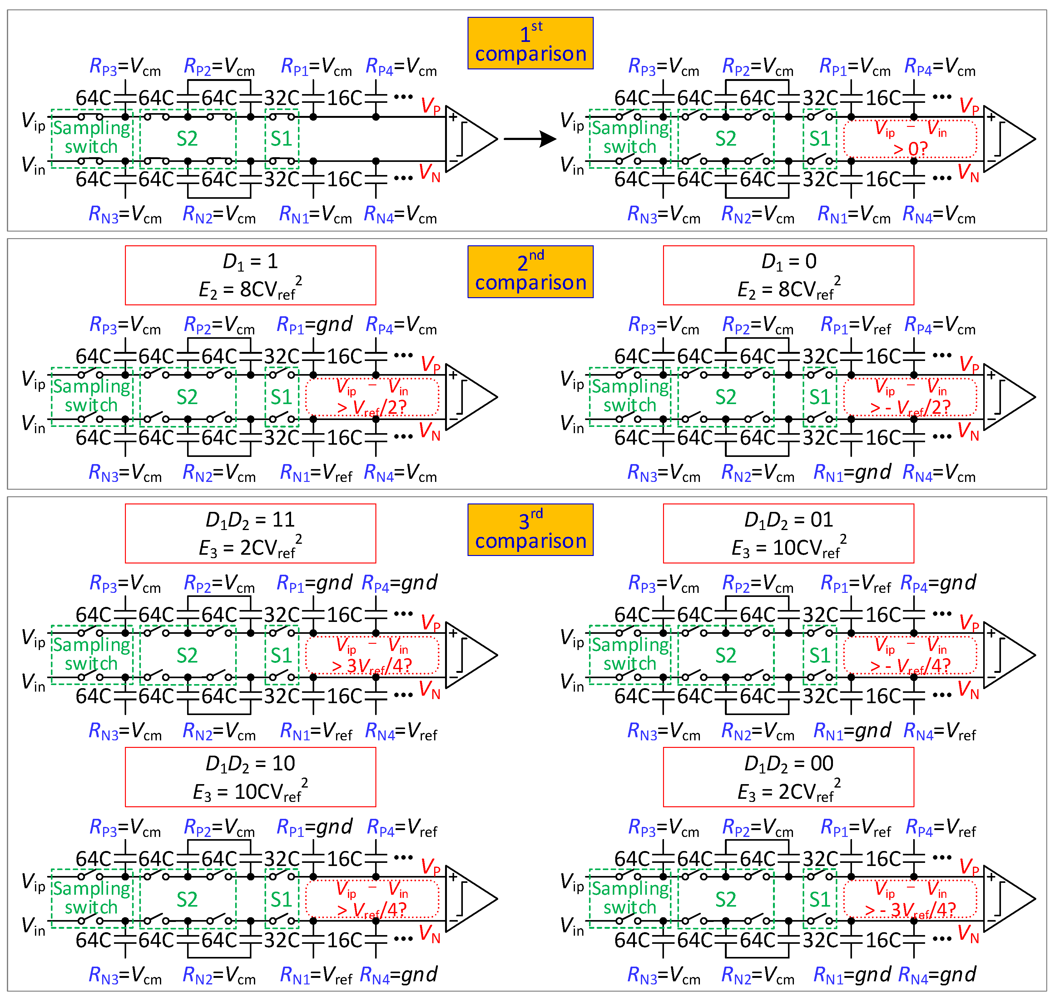
The steps of the conversion process of 8-bit mode are illustrated in Figure 2.
Initially, in the sampling phase, all switches are closed, and the reference voltage of all capacitors is set to Vcm. The input voltage is sampled onto the top plates of the capacitors.
In the 1st comparison, all switches are opened, and the output voltage of the capacitor array is found to be
{ V P ( 1 ) = V i p V N ( 1 ) = V i n
The comparator compares the sampling signals (Vip and Vin) and obtains D1.
In the 2nd comparison, if D1 is 1, the reference voltage of RP1 is changed from Vcm to gnd, and RN1 is changed from Vcm to Vref.. If D1 is 0, the reference voltage of RP1 is changed from Vcm to Vref, and RN1 is changed from Vcm to gnd. The output voltage is found to be
{ V P ( 2 ) = V i p + [ 1 2 D 1 ] V r e f 4 V N ( 2 ) = V i n + [ 2 D 1 1 ] V r e f 4
The comparator compares VP(2) with VN(2) and obtains D2.
In the 3rd comparison, if D2 is 1, the reference voltage of RP4 is changed from Vcm to gnd, and RN4 is changed from Vcm to Vref. If D4 is 0, the reference voltage of RP4 is changed from Vcm to Vref, and RN4 is changed from Vcm to gnd. The output voltage is found to be
{ V P ( 3 ) = V i p + [ 1 2 D 1 ] V r e f 4 + [ 1 2 D 2 ] V r e f 8 V N ( 3 ) = V i n + [ 2 D 1 1 ] V r e f 4 + [ 2 D 2 1 ] V r e f 8
The comparator compares VP(3) with VN(3) and obtains D3.
From the 3rd comparison to the 8th comparison, the DAC performs Vcm-based switching scheme [11].

2.1.2. Proposed 9-Bit Mode Switching Scheme

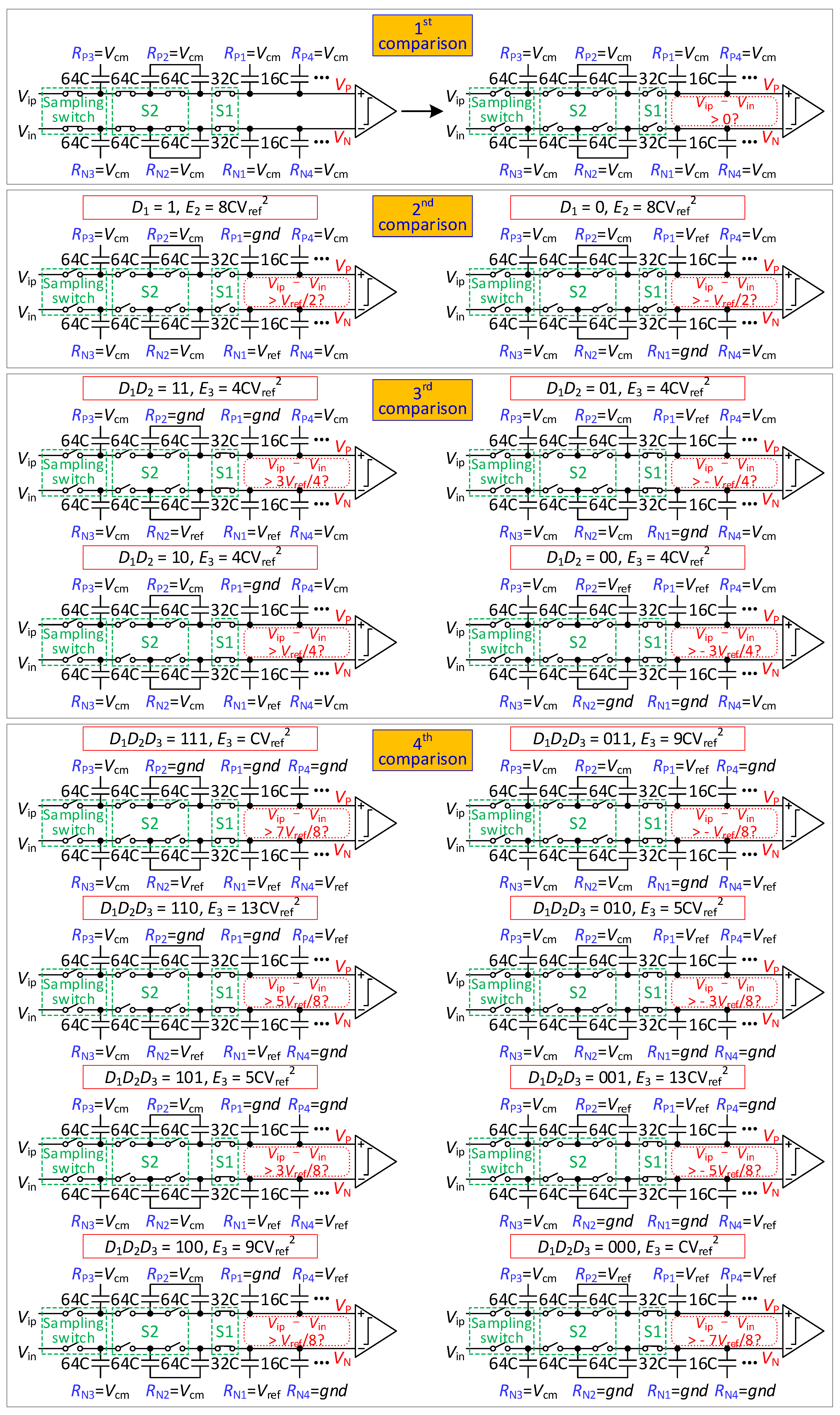
The steps of the conversion process of 9-bit mode are illustrated in Figure 3.
From the sampling phase to the 2nd comparison, a conversion process of 9-bit mode is the same as that of 8-bit mode.
In the 3rd comparison, S1 is closed. If D1D2 is 11, the reference voltage of RP2 is changed from Vcm to gnd, and RN2 is changed from Vcm to Vref. If D1D2 is 00, the reference voltage of RP2 is changed from Vcm to Vref, and RN2 is changed from Vcm to gnd. If D1D2 is 01 or 10, the reference voltage of RP2 and RN2 remains unchanged. The output voltage is shown in equation 3. The comparator compares VP(3) with VN(3) and obtains D3.
In the 4th comparison, if D3 is 1, the reference voltage of RP4 is changed from Vcm to gnd, and RN4 is changed from Vcm to Vref. If D3 is 0, the reference voltage of RP4 is changed from Vcm to Vref, and RN4 is changed from Vcm to gnd. The output voltage is found to be
{ V P ( 4 ) = V i p + [ 1 2 D 1 ] V r e f 4 + [ 1 2 D 2 ] V r e f 8 + [ 1 2 D 3 ] V r e f 16 V N ( 4 ) = V i n + [ 2 D 1 1 ] V r e f 4 + [ 2 D 2 1 ] V r e f 8 + [ 2 D 3 1 ] V r e f 16
The comparator compares VP(4) with VN(4) and obtains D4.
From the 4th comparison to the 9th comparison, the DAC performs a Vcm-based switching scheme [11].

2.1.3. Proposed 10-Bit Mode Switching Scheme

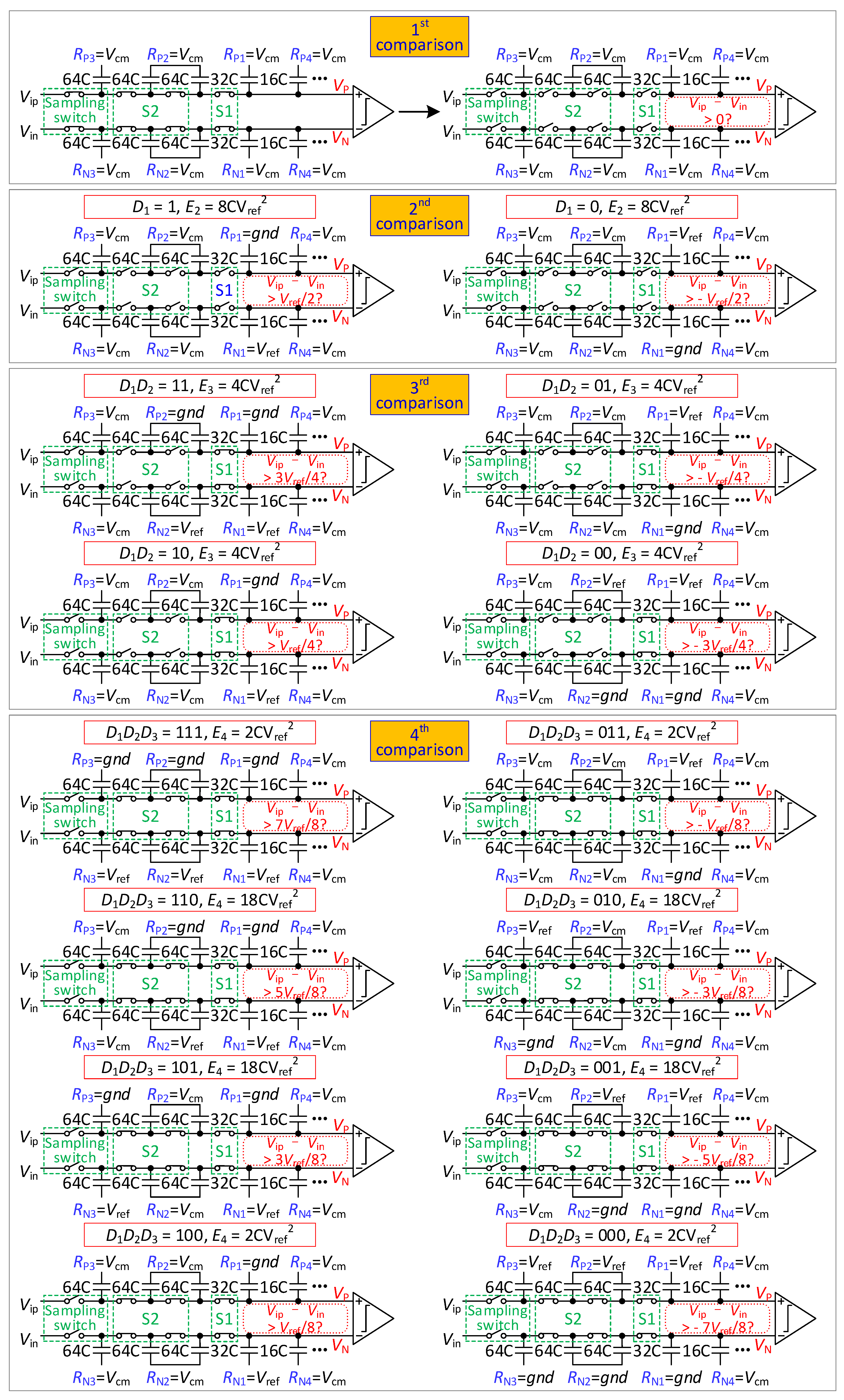
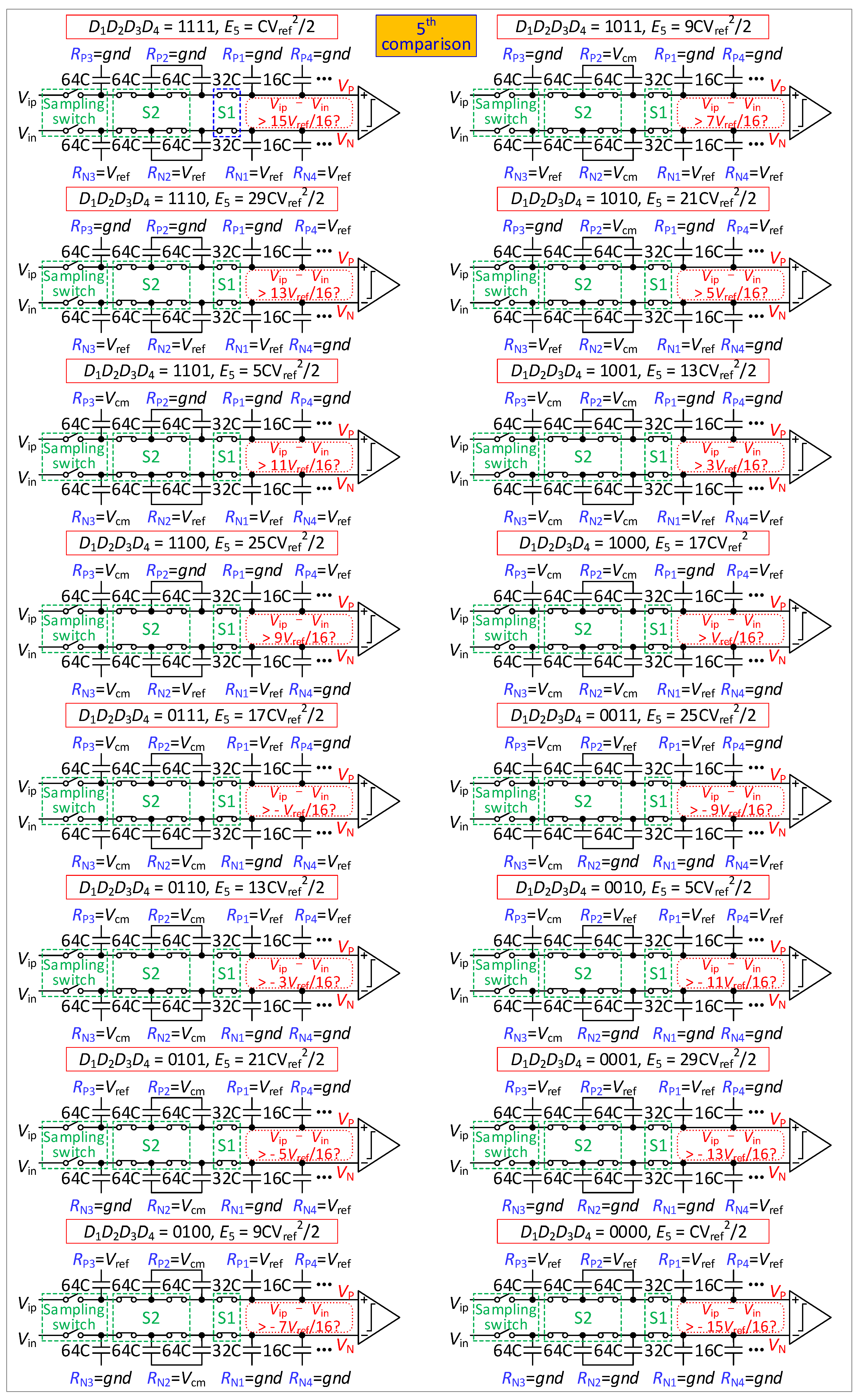
The steps of the conversion process of 10-bit are illustrated in Figure 4 and Figure 5.
From the sampling phase to the 3rd comparison, the conversion process of 10-bit mode is the same as that of 9-bit mode.
In the 4th comparison, S2 is closed. If D1D3 is 11, the reference voltage of RP3 is changed from Vcm to gnd, and RN3 is changed from Vcm to Vref. If D1D3 is 00, the reference voltage of RP3 is changed from Vcm to Vref, and RN3 is changed from Vcm to gnd. If D1D3 is 01 or 10, the reference voltage of RP3 and RN3 remains unchanged. The output voltage is found to be
{ V P ( 4 ) = V i p + [ 1 2 D 1 ] V r e f 4 + [ 1 2 D 2 ] V r e f 8 + [ 1 2 D 3 ] V r e f 16 V N ( 4 ) = V i n + [ 2 D 1 1 ] V r e f 4 + [ 2 D 2 1 ] V r e f 8 + [ 2 D 3 1 ] V r e f 16
The comparator compares VP(4) with VN(4) and obtains D4.
In the 5th comparison, if D4 is 1, the reference voltage of RP4 is changed from Vcm to gnd, and RN4 is changed from Vcm to Vref. If D4 is 0, the reference voltage of RP4 is changed from Vcm to Vref, and RN4 is changed from Vcm to gnd. The output voltage is found to be
{ V P ( 5 ) = V i p + j = 1 4 [ 1 2 D j ] V r e f 2 j + 1 V N ( 5 ) = V i n + j = 1 4 [ 2 D j 1 ] V r e f 2 j + 1
The comparator compares VP(5) with VN(5) and obtains D5.
From the 5th comparison to the 10th comparison, the DAC performs a Vcm-based switching scheme [11]. Because the large capacitor does not participate in the first and second comparisons, it is more energy-efficient than a Vcm-based switching scheme.
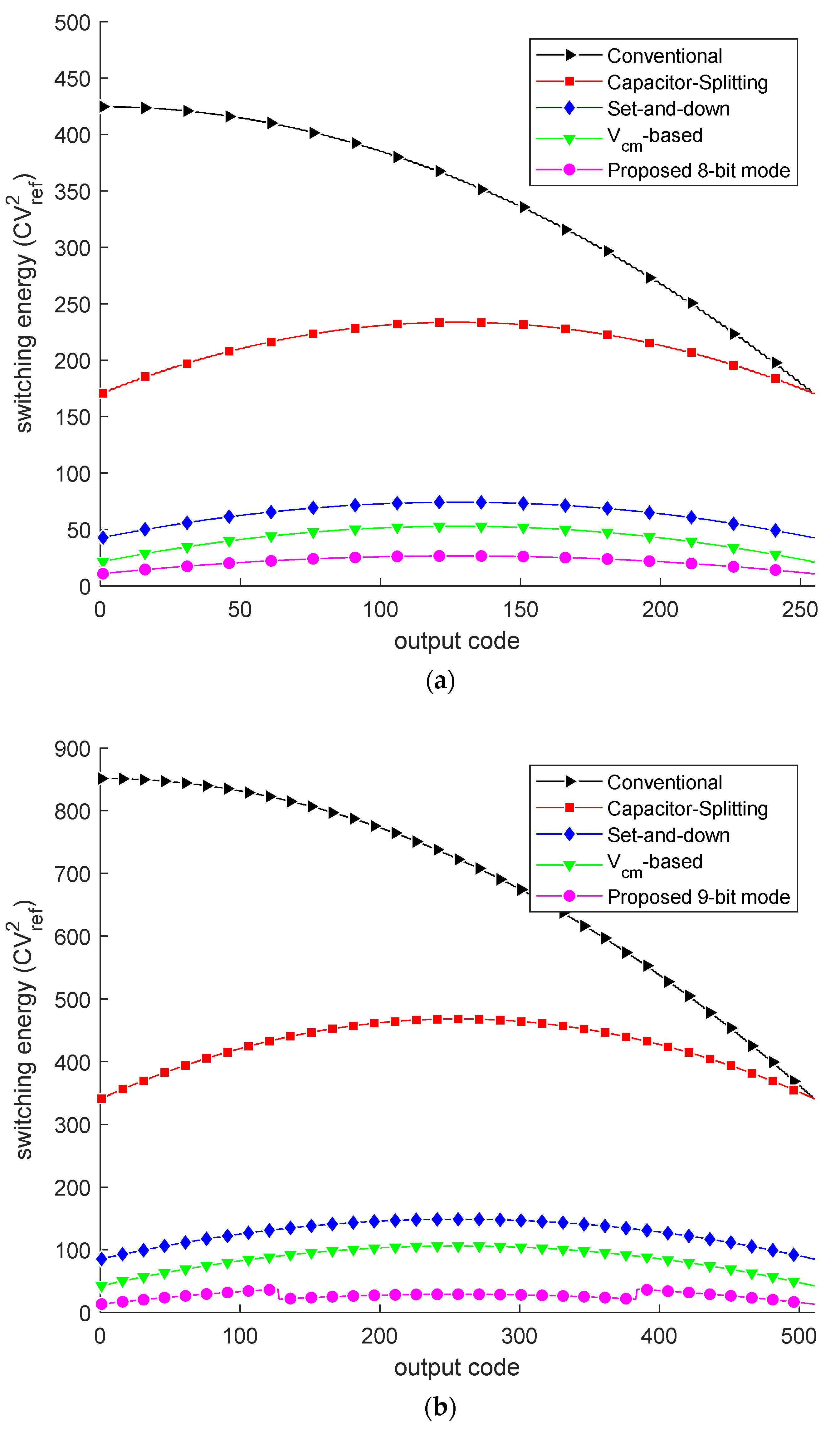
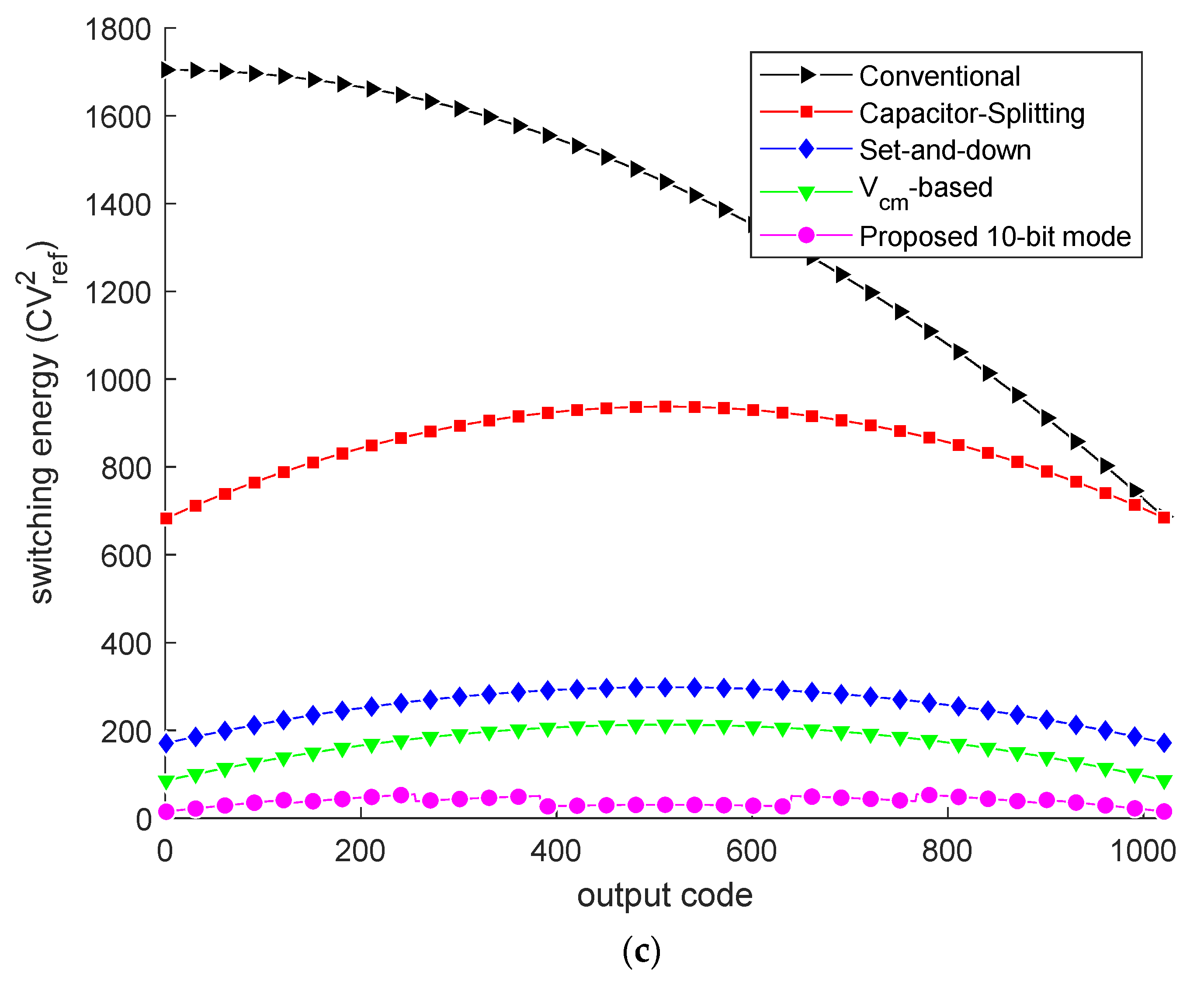
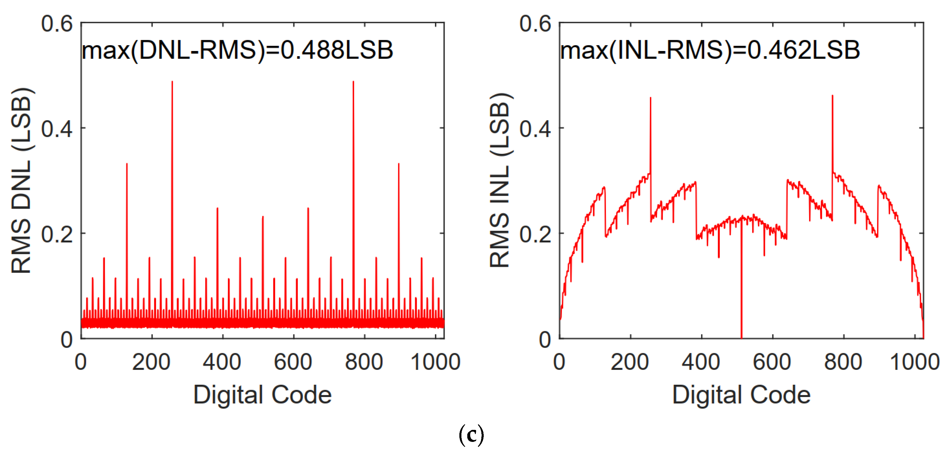
Based on the switching energy calculation method in [9], the switching energy of different switching schemes is calculated and shown in Figure 6 and Table 5. Figure 6 shows switching energy at each output code for different switching schemes. Benefiting from the resolution-reconfigurable technology, the proposed switching scheme has lower switching energy in middle output codes for the 9-bit and 10-bit modes. As shown in Table 5 for the proposed switching scheme, the more bits, the more energy is saved; the scheme saves 96.1% and 97.3% of switching energy in 9-bit and 10-bit modes, respectively. Figure 7 presents the 500-run Monte Carlo simulation results of the proposed DAC switching scheme with unit capacitor mismatch of σu/Cu = 2%. The RMS DNL and the RMS INL of the proposed DAC switching scheme are 0.214/0.280/0.488 LSB and 0.218/0.278/0.462 LSB, corresponding to the 8/9/10-bit mode, respectively.

2.2. Sampling Switch

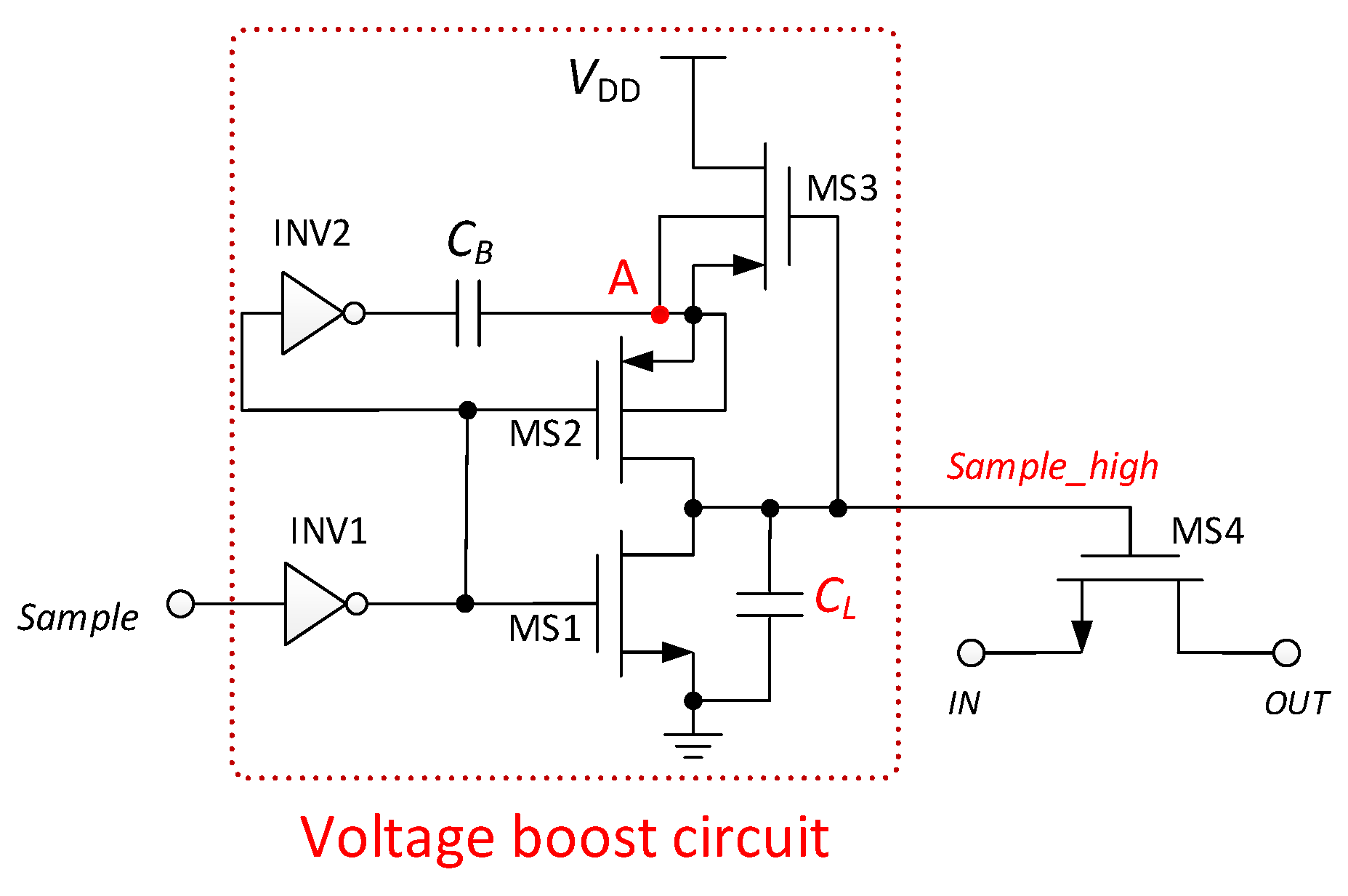
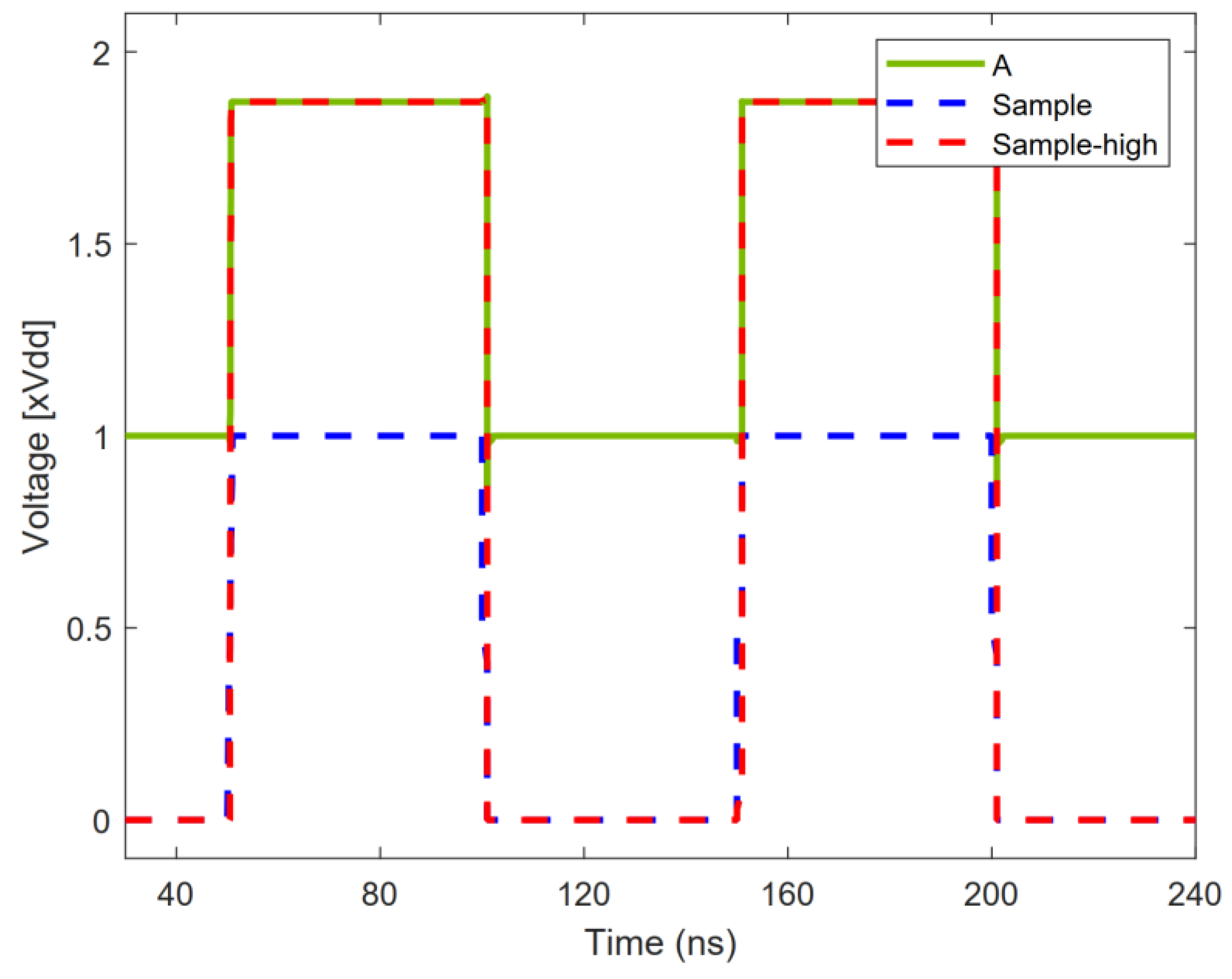
In order to reduce the on-resistance of the sampling switch and reduce the sampling error, the sampling switch adopts a bootstrap switch circuit [13]. The voltage bootstrap sampling circuit is shown in Figure 8. When the “Sample” voltage is low, the transistors MS1 and MS3 are turned on, MS2 and MS4 are turned off, the voltage of node A is charged to VDD, and the “Sample_high” voltage is low. When the “Sample” voltage becomes high, the transistor MS1 is turned off, MS2 is turned on, MS3 is turned off, and MS4 is turned on; the voltage of node A is boosted to 2VDD by the capacitor CB, and the “Sample_high” voltage starts to increase. The “Sample_high” voltage boost expression is as follows:
V s a m p l e _ h i g h = 2 V D D C B C B + C L
CL is the parasitic capacitance. If CB is much larger than CL, the “Sample_high” voltage is raised to about twice VDD.
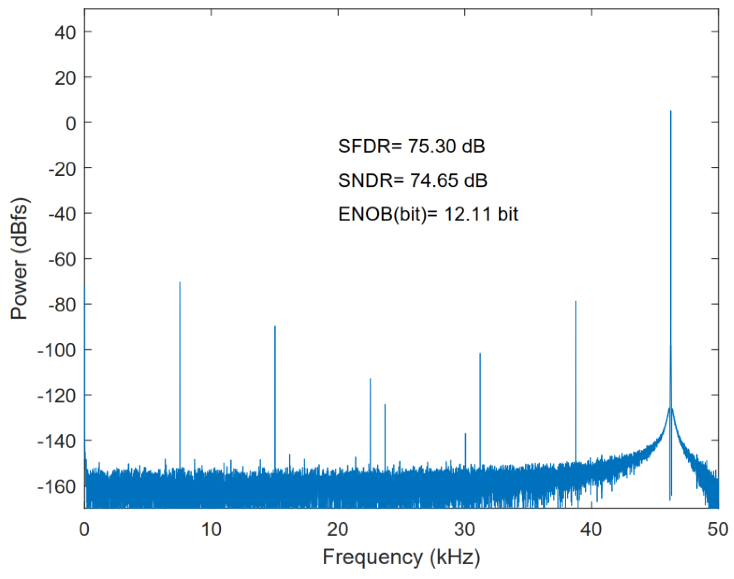
Figure 9 illustrates the voltage bootstrap of the sampling switch. The FFT of the sampling switch is shown in Figure 10. The spurious-free dynamic range (SFDR) and the signal-to-noise-plus-distortion ratio (SNDR) of the sampling switch are 75.30 and 74.65 dB, respectively.

2.3. Comparator

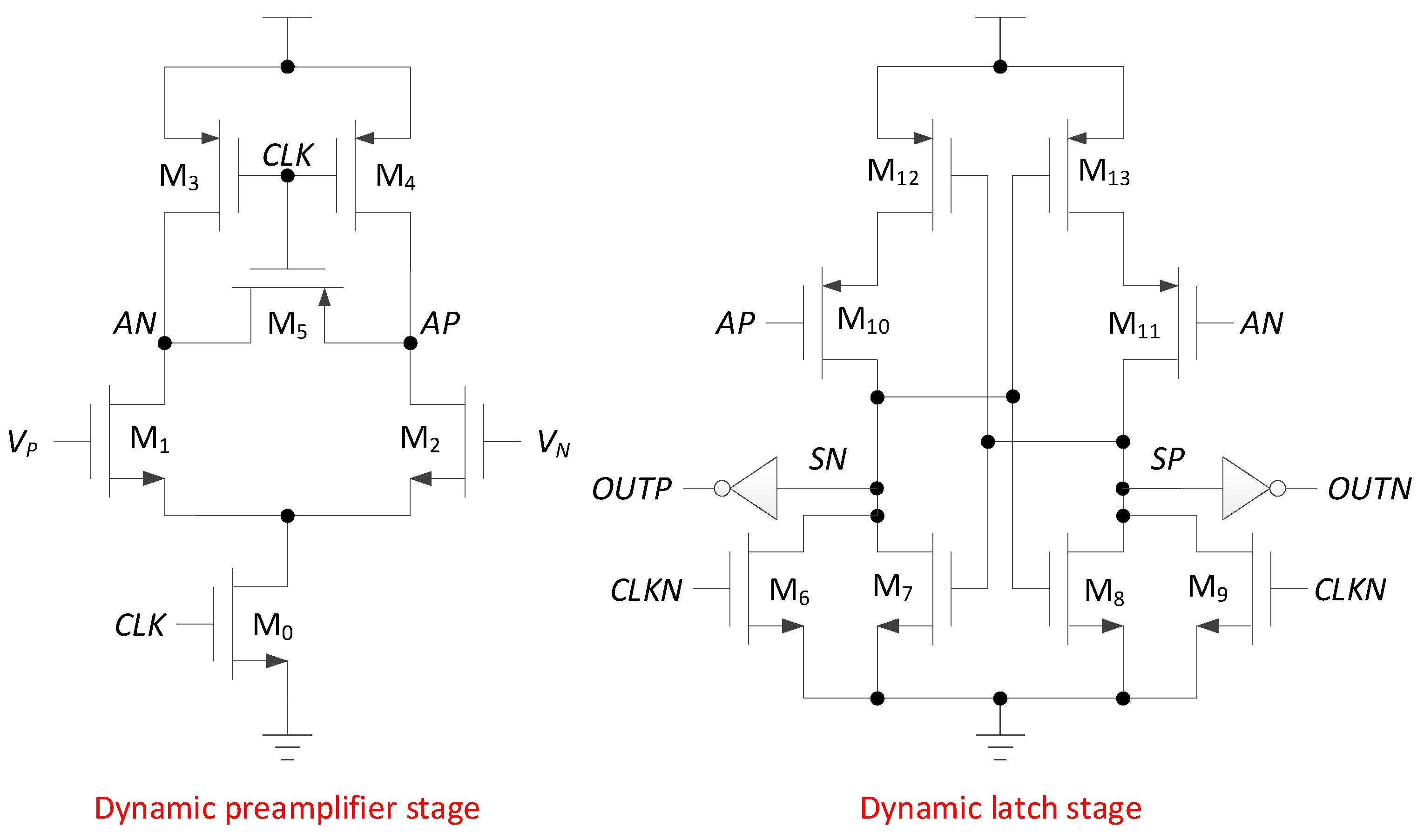
To decrease the power consumption of the comparator, a two-stage full dynamic comparator [14] is used. Figure 11 shows the schematic diagram of the comparator. The first stage is the dynamic preamplifier stage, and VP and VN are the output signals of the capacitor array DAC, connected to the differential input of the comparator. AN and AP are differential outputs of the dynamic preamplifier stage. The second stage is the dynamic latch stage, which is responsible for the two-stage amplification and the result latch, and OUTP and OUTN are the comparison results.
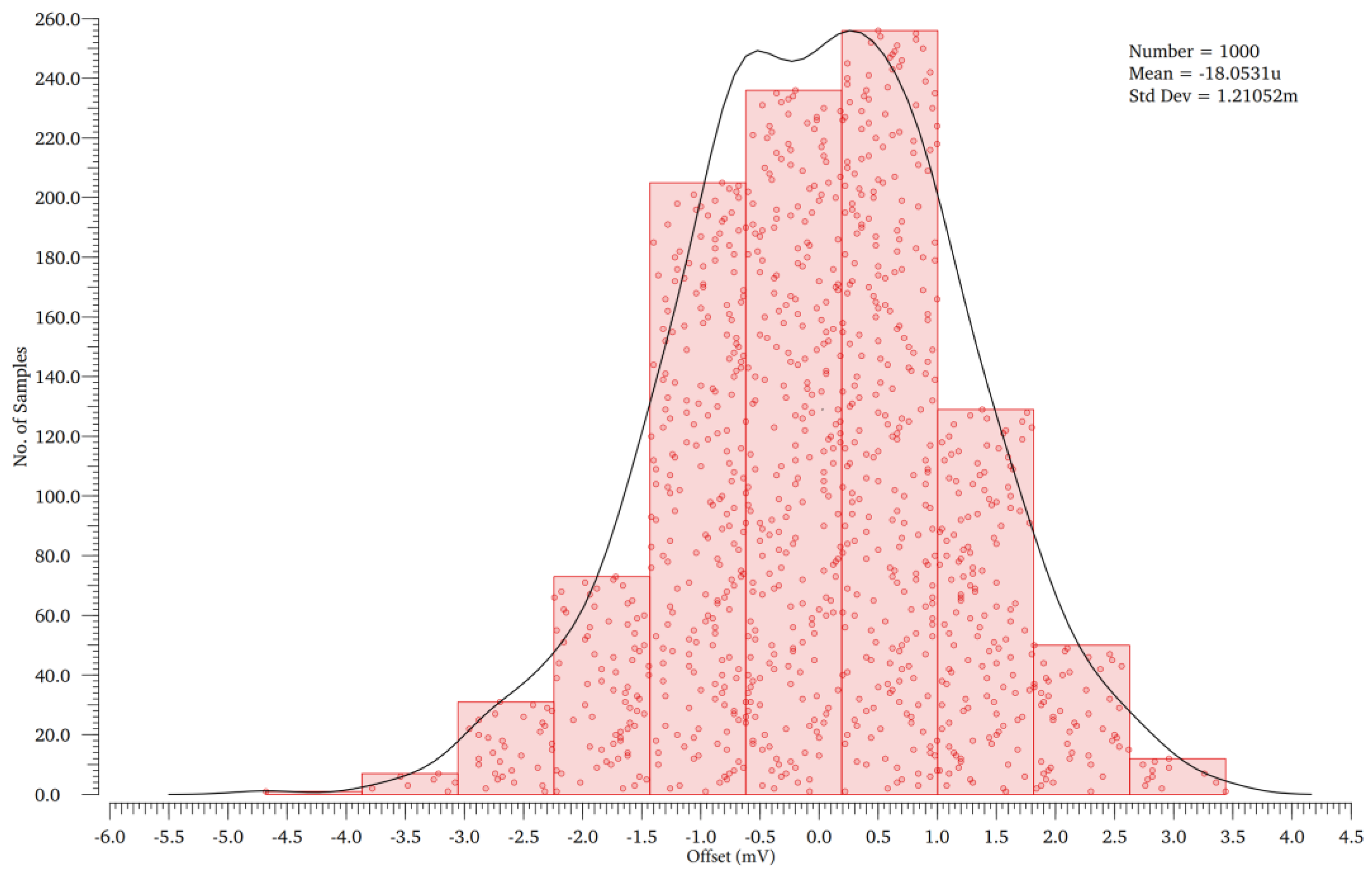
When CLK is low (CLKN is high), M0 is off, M3 and M4 are on, AN and AP are charged to high (M5 makes AP and AN charge balance), M6 and M9 are on, OUTP and OUTN are pulled up to high. When CLK is high (CLKN is low), M3, M4 and M5 are turned off, M0 is turned on, AN and AP are discharged through M1 and M2, respectively, and the speed of discharge depends on the voltage of VP and VN (if VP > VN, then AP > AN; if VP < VN, then AP < AN). At this time, M6 and M9 of the dynamic latch stage are turned off, SP and SN are charged by M10 and M11, and the charging speed depends on the voltage of AP and AN (if AP > AN, then SP > SN; if AP < AN, then SP < SN). If SP or SN rises to the threshold voltage, M7 or M8 will be turned on, positive feedback will start to work, and one of SP and SN quickly rises to high and the other pulls low to complete the latching of the comparison result. Since the dynamic comparator does not form a power-to-ground path when operating, the comparator has only dynamic power. The transient simulation of the comparator is shown in Figure 12. Figure 13 shows the Monte Carlo simulations that are performed to observe the effect of mismatches and process variations on offset voltage. Offset voltage has a mean value of −18.053 µV with the standard deviation (SD) of 1.21052 mV.

2.4. SAR Control Logic

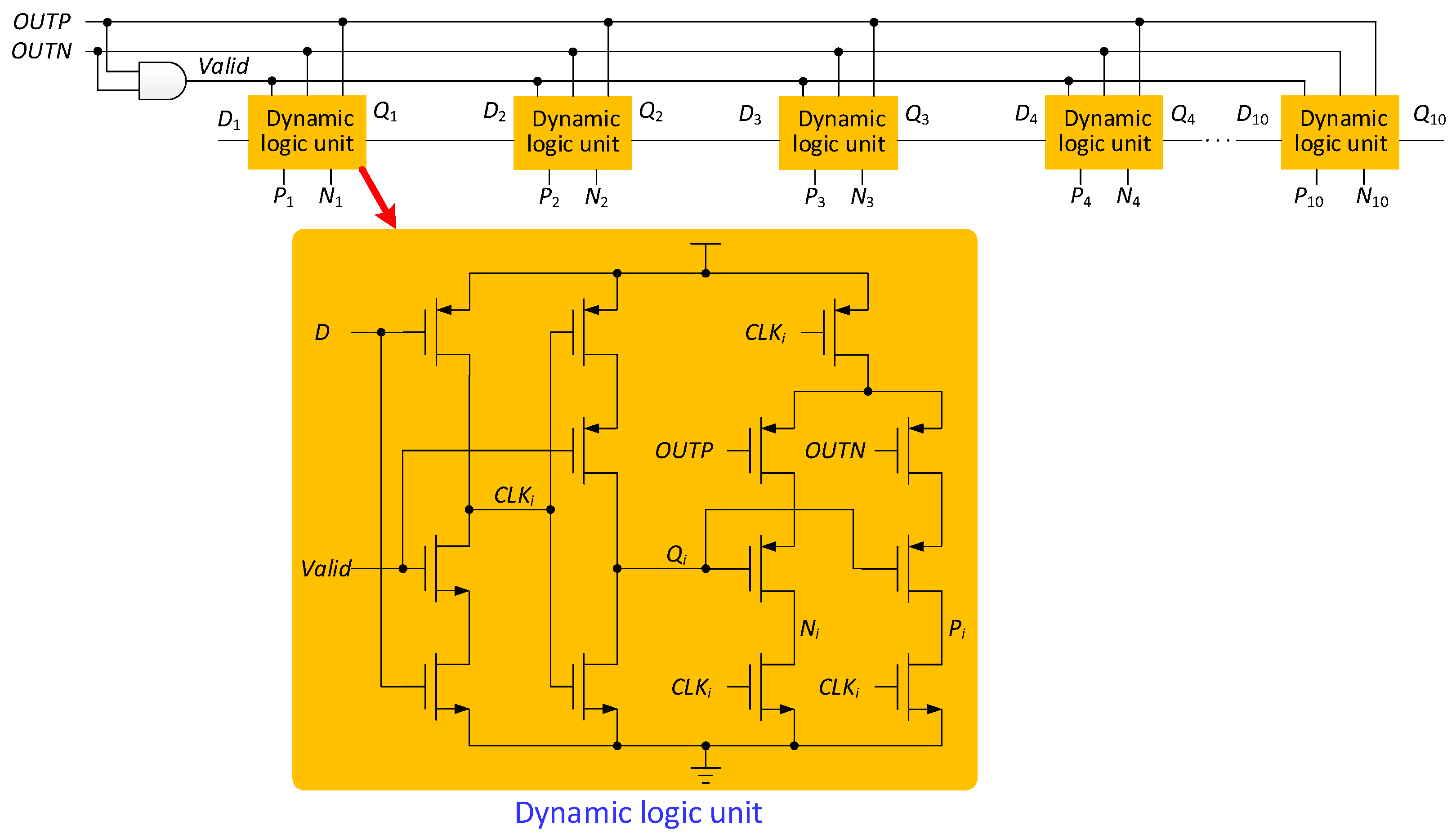
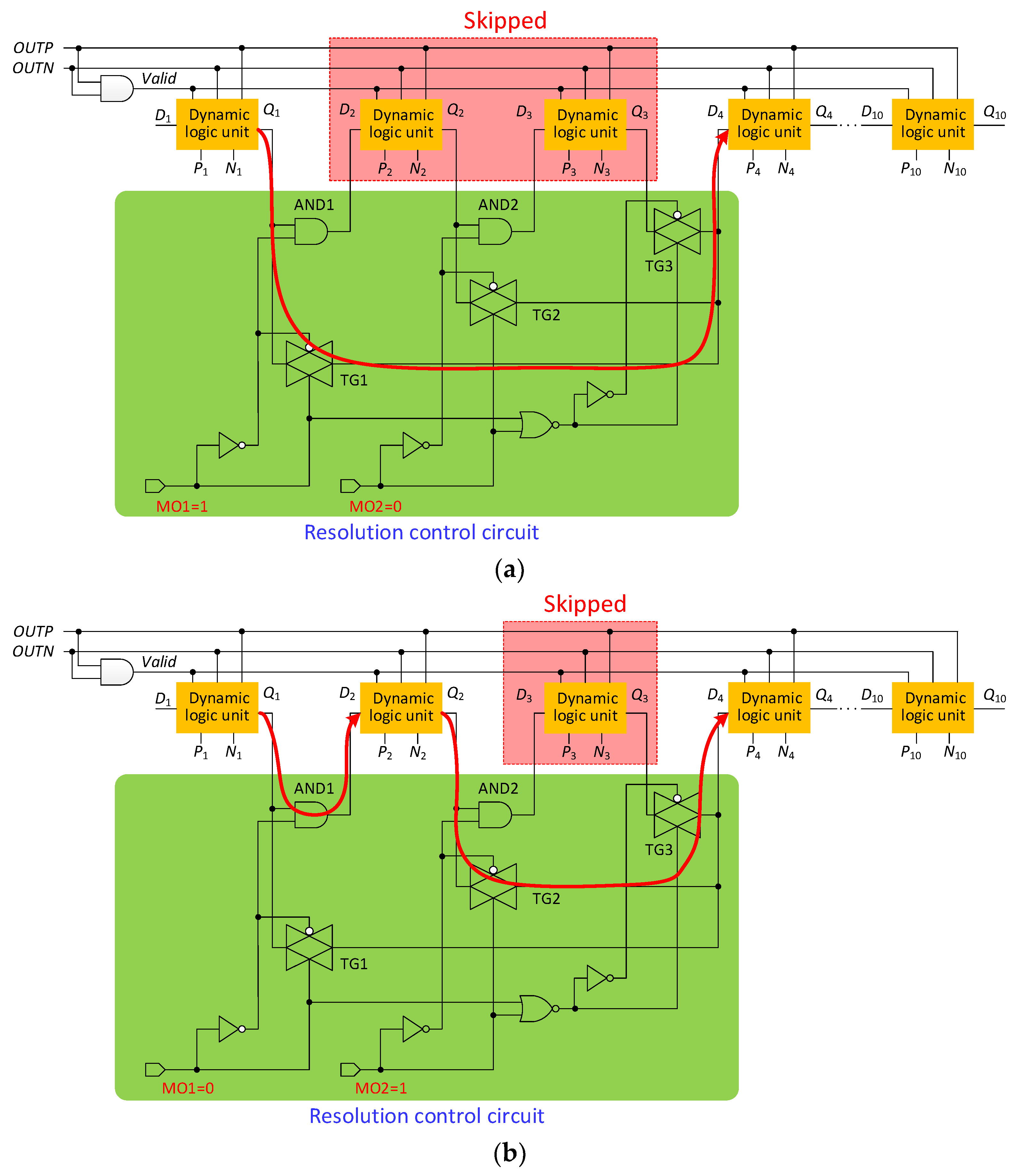
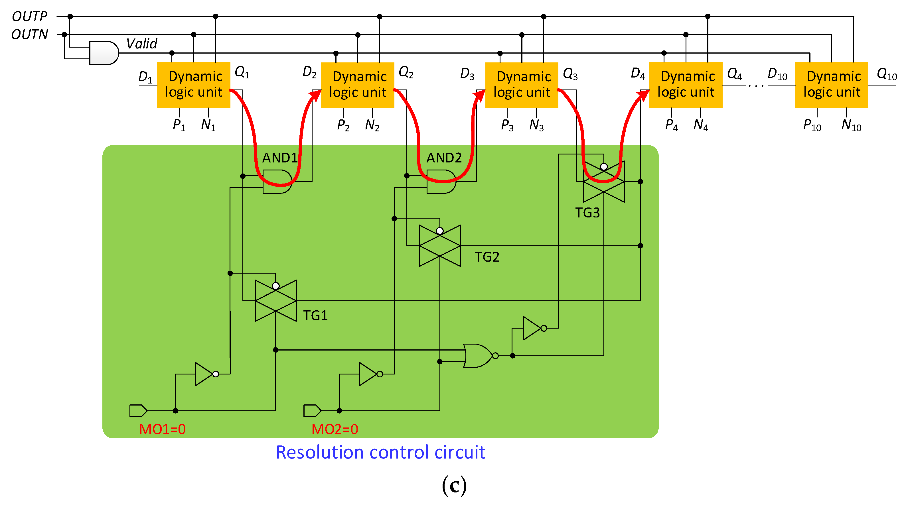
To improve the performance of SAR logic, a dynamic logic unit is used [15]. As shown in Figure 14, the SAR logic is composed of dynamic logic units, one by one. The dynamic logic unit has both a shift function and a function of storing comparison results, which saves many transistors compared to conventional shift registers. The 10-bit SAR logic has 10 dynamic logic units. When the SAR ADC is operating in 8-bit or 9-bit resolutions, in order to save power, two or one dynamic logic units need to be skipped, respectively. As shown in Figure 15, a resolution control circuit is added to SAR logic. The resolution of SAR logic is controlled by MO1 and MO2. Different resolutions will form different circuit paths. The resolution settings are shown in Table 6.
Figure 15a shows the 8-bit mode work diagram of SAR control logic. When MO1 = 1 and MO2 = 0, the circuit is set to 8-bit operating mode, the transmission gate TG1 is turned on, the AND gates AND1 and AND2 are turned off, and the transmission gates TG2 and TG3 are turned off. Then, the output Q1 of the first dynamic logic unit is directly connected to the input D4 of the fourth dynamic logic unit; the second and third dynamic logic units are skipped.
Figure 15b shows the 9-bit mode work diagram of SAR control logic. When MO1 = 0 and MO2 = 1, the circuit is set to 9-bit operating mode, AND1 and TG2 are turned on, and AND2, TG1, and TG3 are turned off. Then, the output Q2 of the second dynamic logic unit is directly connected to the input D4 of the fourth dynamic logic unit; the third dynamic logic unit is skipped.
Figure 15c shows the 10-bit mode work diagram of SAR control logic. When MO1 = 0 and MO2 = 0, the circuit is set to 10-bit operating mode, AND1, AND2 and TG3 are turned on, and TG1 and TG2 are turned off. In this case, no dynamic logic cells are skipped.

3. Results

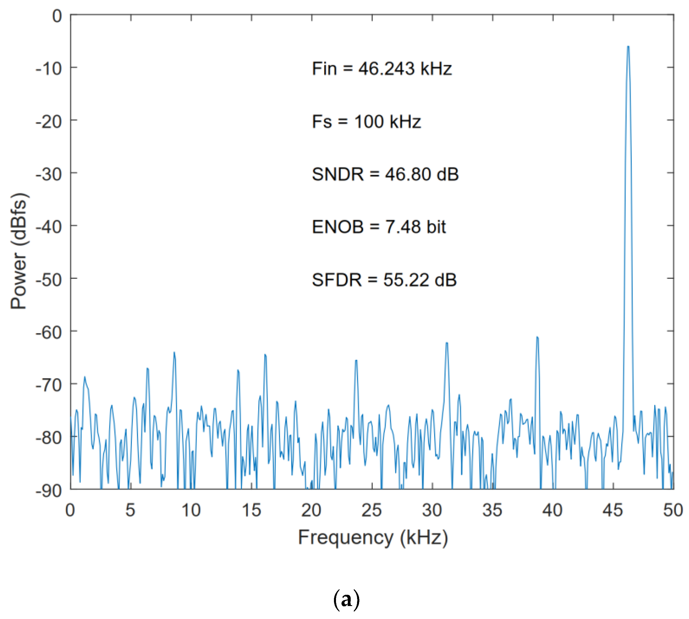
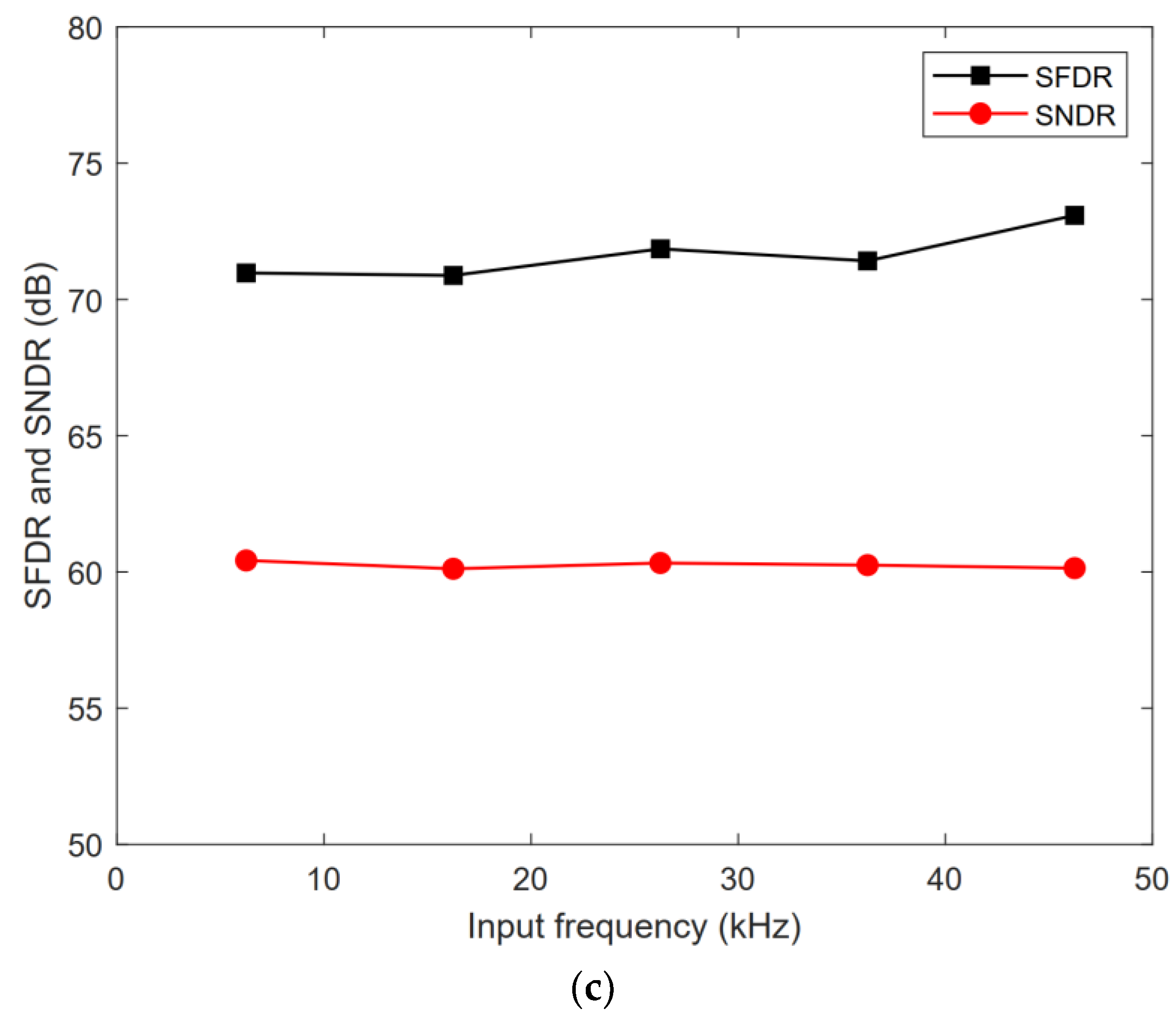
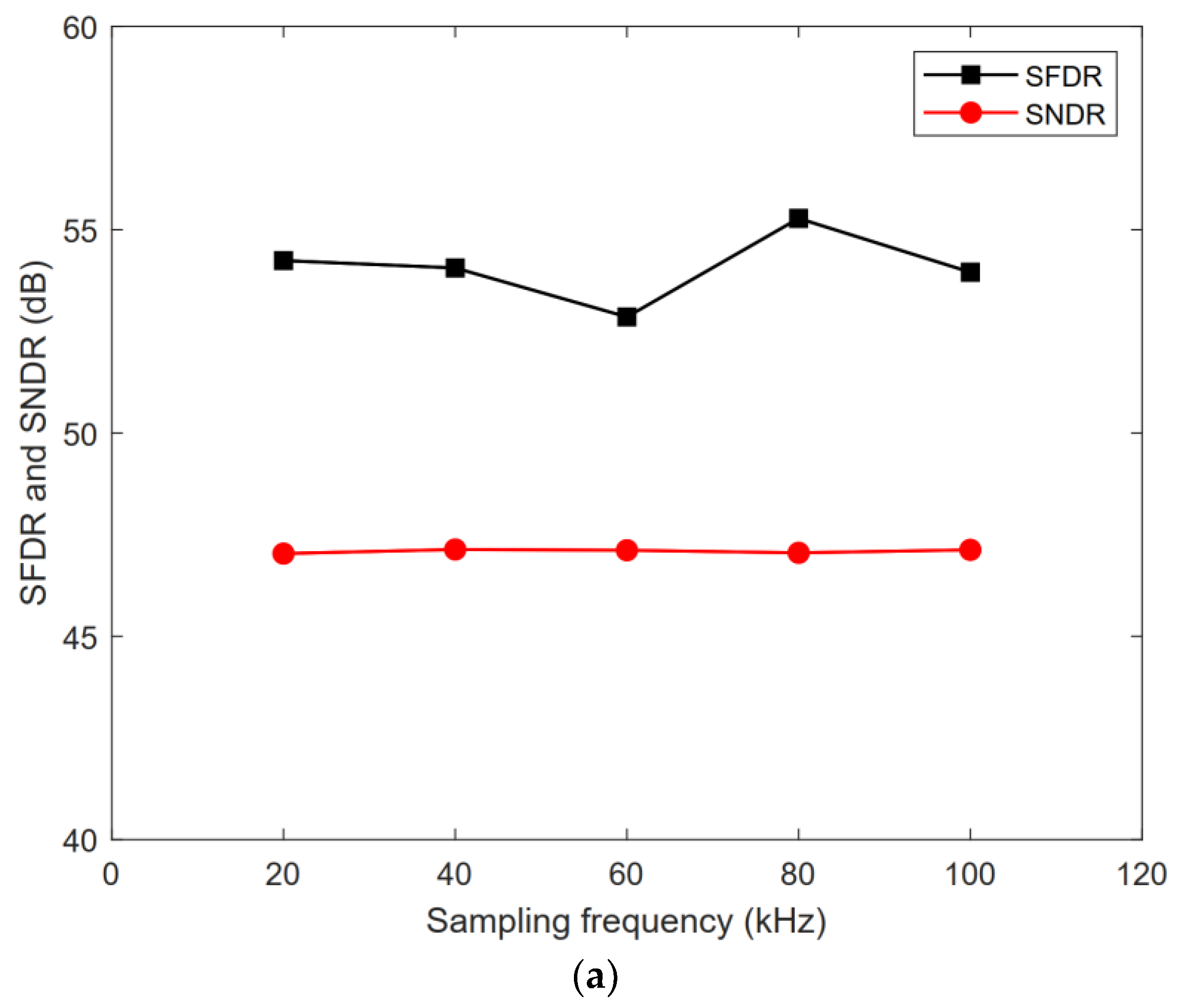
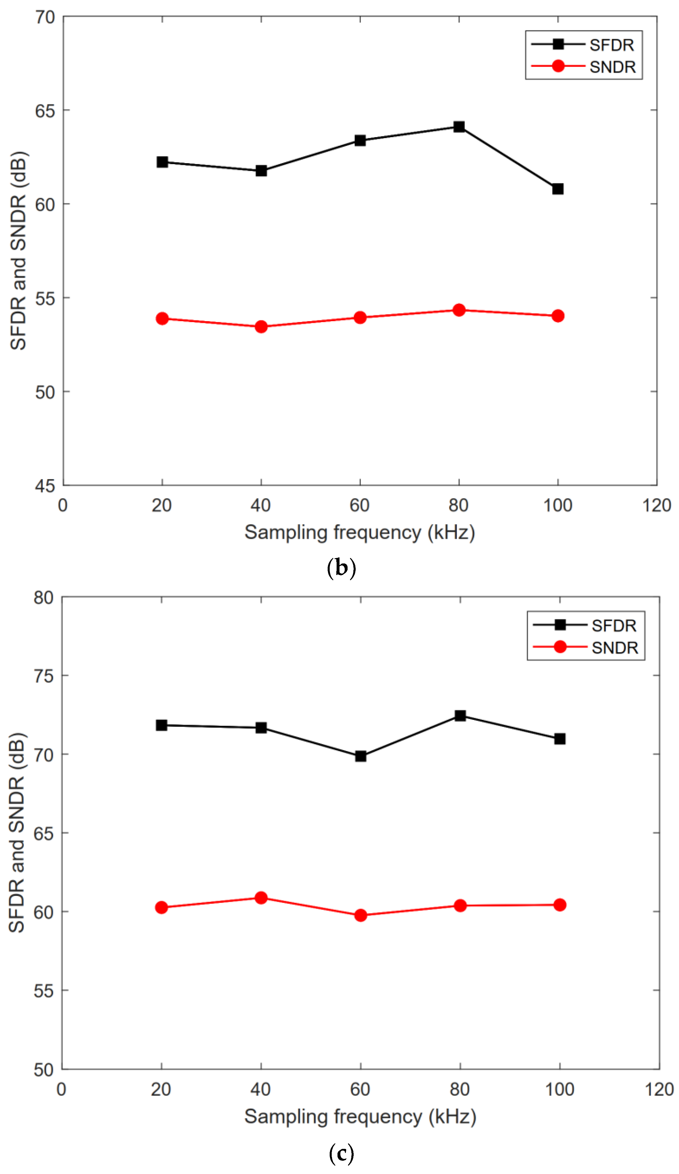
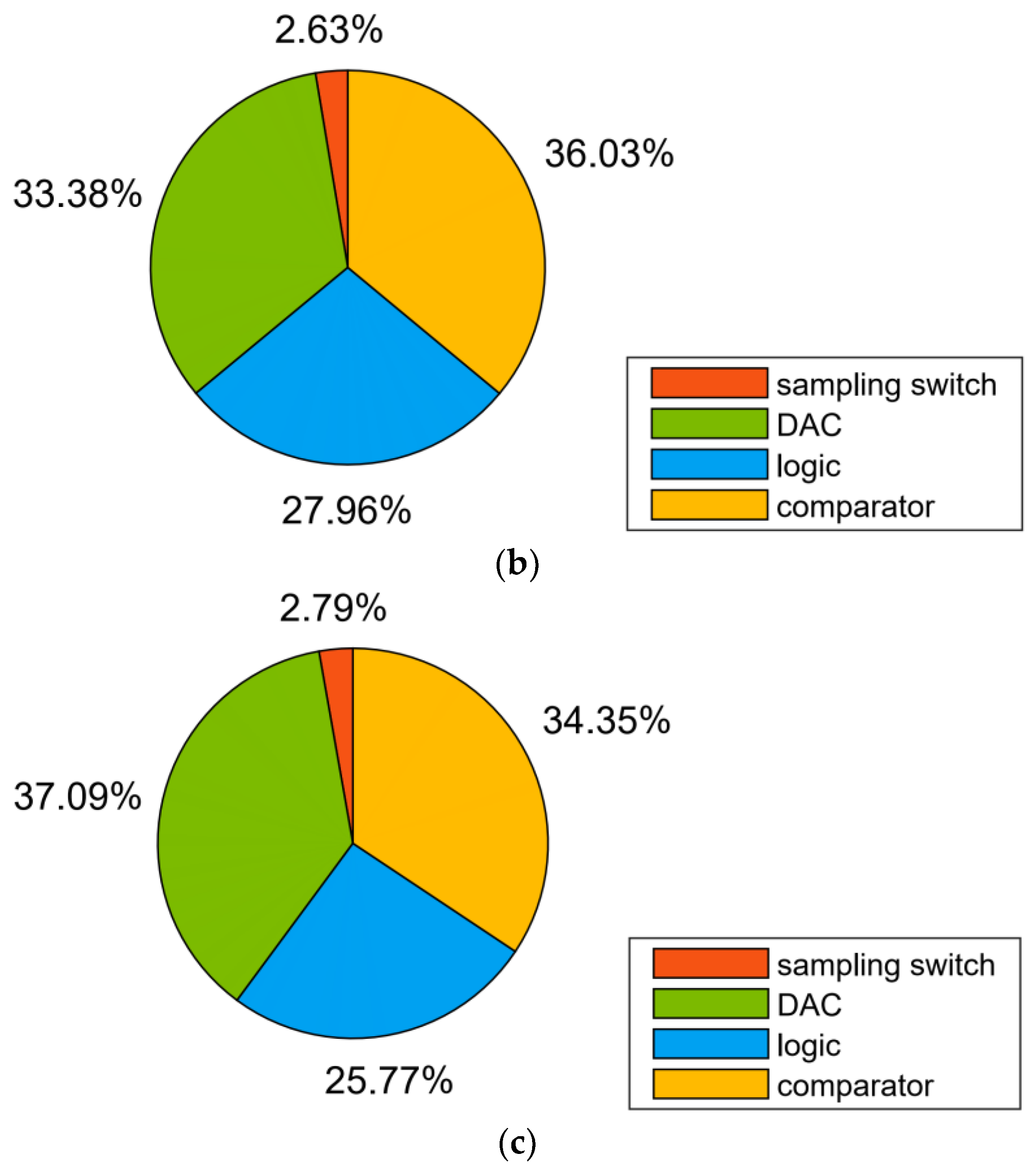
The proposed ADC was designed and post-simulated using 180 nm CMOS technology. Figure 16 shows the layout of the ADC with a total area of 360 μm × 325 μm. Figure 17 shows the FFT spectrum of the proposed ADC in 8-bit, 9-bit, and 10-bit modes with the 1.8 V full swing inputs at 46.243 kHz and the sampling rate at 100 kS/s; the ADC achieves the 46.80/53.89/60.14 dB signal-to-noise and distortion ratio (SNDR) and 55.22/62.51/73.09 dB spurious-free dynamic range (SFDR), respectively. Figure 18 shows the SNDR and SFDR of the proposed SAR ADC with respect to the input frequency. Figure 19 shows the SNDR and SFDR of the proposed SAR ADC with respect to the sampling frequency. The proposed ADC consumes 0.81/0.91/1.01 μW corresponding to the 8/9/10-bit mode, respectively. Figure 20 shows the power breakdown of the ADC.
Table 7 compares the proposed ADC with other ADCs [16,17,18,19]. As shown in Table 7, the performance of the proposed ADC is still competitive when it is implemented in 0.18 μm 1.8 V CMOS process. The Figure-of-Merit (FoM) was calculated from the following equation:
F o M = P o w e r 2 E N O B × f s a m p i n g

4. Conclusions

In this paper, a reconfigurable 8–10-bit SAR ADC with an energy-efficient DAC switching scheme for biosensor applications is presented. Several techniques are used to enable the reconfiguration. Simulated with a 180 nm CMOS process and 100 kS/s sampling rate, the ADC achieves the 46.80/53.89/60.14 dB SNDR, the 55.22/62.51/73.09 dB SFDR, and the 0.81/0.91/1.01 μW power consumption in 8/9/10-bit mode, respectively.

Author Contributions

Conceptualization, Y.H.; methodology, Y.H.; software, Y.H. and B.T.; validation, Y.H., L.H. and B.T.; formal analysis, Y.H.; investigation, Y.H.; resources, Y.H., B.L. and Z.W.; data curation, Y.H. and L.H.; writing—original draft preparation, Y.H.; writing—review and editing, B.L., L.H. and X.L.; visualization, Y.H., B.T. and L.H.; supervision, Y.H. and B.L.; project administration, Y.H.; funding acquisition, Y.H. All authors have read and agreed to the published version of the manuscript.

Funding

This research was funded by the National Natural Science Foundation of China under Grant (no. 62174058), the Key Field Project of Colleges and Universities in Guangdong Province (no. 2021ZDZX1081, 2022ZDZX1044), the Key Project of Social Welfare and Basic Research Project in Zhongshan City (no. 2021B2020), the Construction Project of Professional Quality Engineering in 2020 (no. YLZY202001), and the Construction Project of Professional Quality Engineering in 2021 (no. JD202101).

Data Availability Statement

Not applicable.

Conflicts of Interest

The authors declare no conflict of interest.

References

  1. Wang, S.; Hung, C. A 0.3V 10b 3MS/s SAR ADC with Comparator Calibration and Kickback Noise Reduction for Biomedical Applications. IEEE Trans. Biomed. Circuits Syst. 2020, 14, 558–569. [Google Scholar] [CrossRef] [PubMed]
  2. Tong, X.; Song, M.; Chen, Y.; Dong, S. A 10-Bit 120 kS/s SAR ADC without Reset Energy for Biomedical Electronics. Circuits Syst. Signal Process. 2019, 38, 5411–5425. [Google Scholar] [CrossRef]
  3. Mao, W.; Li, Y.; Heng, C.; Lian, Y. A Low Power 12-bit 1-kS/s SAR ADC for Biomedical Signal Processing. IEEE Trans. Circuits Syst. I Regul. Pap. 2019, 66, 477–488. [Google Scholar] [CrossRef]
  4. Sadollahi, M.; Hamashita, K.; Sobue, K.; Temes, G.C. An 11-Bit 250-nW 10-kS/s SAR ADC with Doubled Input Range for Biomedical Applications. IEEE Trans. Circuits Syst. I Regul. Pap. 2018, 65, 61–73. [Google Scholar] [CrossRef]
  5. Chen, Y.; Zhuang, Y.; Tang, H. A highly energy-efficient, area-efficient switching scheme for SAR ADC in biomedical applications. Analog Integr. Circuits Signal Process. 2019, 101, 133–143. [Google Scholar] [CrossRef]
  6. Zhu, Z.; Qiu, Z.; Liu, M.; Ding, R. A 6-to-10-Bit 0.5 V-to-0.9 V Reconfigurable 2 MS/s Power Scalable SAR ADC in 0.18 µm CMOS. IEEE Trans. Circuits Syst. I Regul. Pap. 2015, 62, 689–696. [Google Scholar] [CrossRef]
  7. Yip, M.; Chandrakasan, A.P. A Resolution-Reconfigurable 5-to-10-Bit 0.4-to-1 V Power Scalable SAR ADC for Sensor Applications. IEEE J. Solid-State Circuits 2013, 48, 1453–1464. [Google Scholar] [CrossRef] [Green Version]
  8. O’Driscoll, S.; Shenoy, K.V.; Meng, T.H. Adaptive Resolution ADC Array for an Implantable Neural Sensor. IEEE Trans. Biomed. Circuits Syst. 2011, 5, 120–130. [Google Scholar] [CrossRef] [PubMed] [Green Version]
  9. Ginsburg, B.P.; Chandrakasan, A.P. An energy-efficient charge recycling approach for a SAR converter with capacitive DAC. In Proceedings of the 2005 IEEE International Symposium on Circuits and Systems, Kobe, Japan, 23–26 May 2005; pp. 184–187. [Google Scholar]
  10. Liu, C.C.; Chang, S.J.; Huang, G.Y.; Lin, Y.Z. A 10-bit 50-MS/s SAR ADC with a Monotonic Capacitor Switching Procedure. IEEE J. Solid-State Circuits 2010, 45, 731–740. [Google Scholar] [CrossRef]
  11. Yan, Z.; Chi-Hang, C.; Chio, U.F.; Sai-Weng, S.; Seng-Pan, U.; Martins, R.P.; Maloberti, F. A 10-bit 100-MS/s Reference-Free SAR ADC in 90 nm CMOS. IEEE J. Solid-State Circuits 2010, 45, 1111–1121. [Google Scholar] [CrossRef]
  12. Johns, D.; Martin, K. Analog Integrated Circuit Design; John Wiley & Sons, Inc.: New York, NY, USA, 1997. [Google Scholar]
  13. Rabuske, T.; Fernandes, J. A SAR ADC with a MOSCAP-DAC. IEEE J. Solid-State Circuits 2016, 51, 1410–1422. [Google Scholar] [CrossRef]
  14. Harpe, P.; Cantatore, E.; van Roermund, A. A 10b/12b 40 kS/s SAR ADC with Data-Driven Noise Reduction Achieving up to 10.1b ENOB at 2.2 fJ/Conversion-Step. IEEE J. Solid-State Circuits 2013, 48, 3011–3018. [Google Scholar] [CrossRef]
  15. Zhu, Z.; Xiao, Y.; Wang, W.; Wang, Q.; Yang, Y. A 0.6 V 100 KS/s 8-10 b resolution configurable SAR ADC in 0.18 mu m CMOS. Analog Integr. Circuits Signal Process. 2013, 75, 335–342. [Google Scholar] [CrossRef]
  16. Tang, H.; Sun, Z.C.; Chew, K.W.R.; Siek, L. A 1.33 µW 8.02-ENOB 100 kS/s Successive Approximation ADC with Supply Reduction Technique for Implantable Retinal Prosthesis. IEEE Trans. Biomed. Circuits Syst. 2014, 8, 844–856. [Google Scholar] [CrossRef] [PubMed]
  17. Yuan, C.; Ng, K.A.; Xu, Y.P.; Yen, S.C.; Thakor, N.V. A 1-V 9.8-ENOB 100-kS/s single-ended SAR ADC with symmetrical DAC switching technique for neural signal acquisition. In Proceedings of the 2015 IEEE Asian Solid-State Circuits Conference (A-SSCC), Xiamen, China, 9–11 November 2015. [Google Scholar] [CrossRef]
  18. Wang, J.; Hua, Y.; Zhu, Z. A 10-bit reconfigurable ADC with SAR/SS mode for neural recording. Analog Integr. Circuits Signal Process. 2019, 101, 297–305. [Google Scholar] [CrossRef]
  19. Ro, D.; Min, C.; Kang, M.; Chang, I.J.; Lee, H.-M. A Radiation-Hardened SAR ADC with Delay-Based Dual Feedback Flip-Flops for Sensor Readout Systems. Sensors 2019, 20, 171. [Google Scholar] [CrossRef]
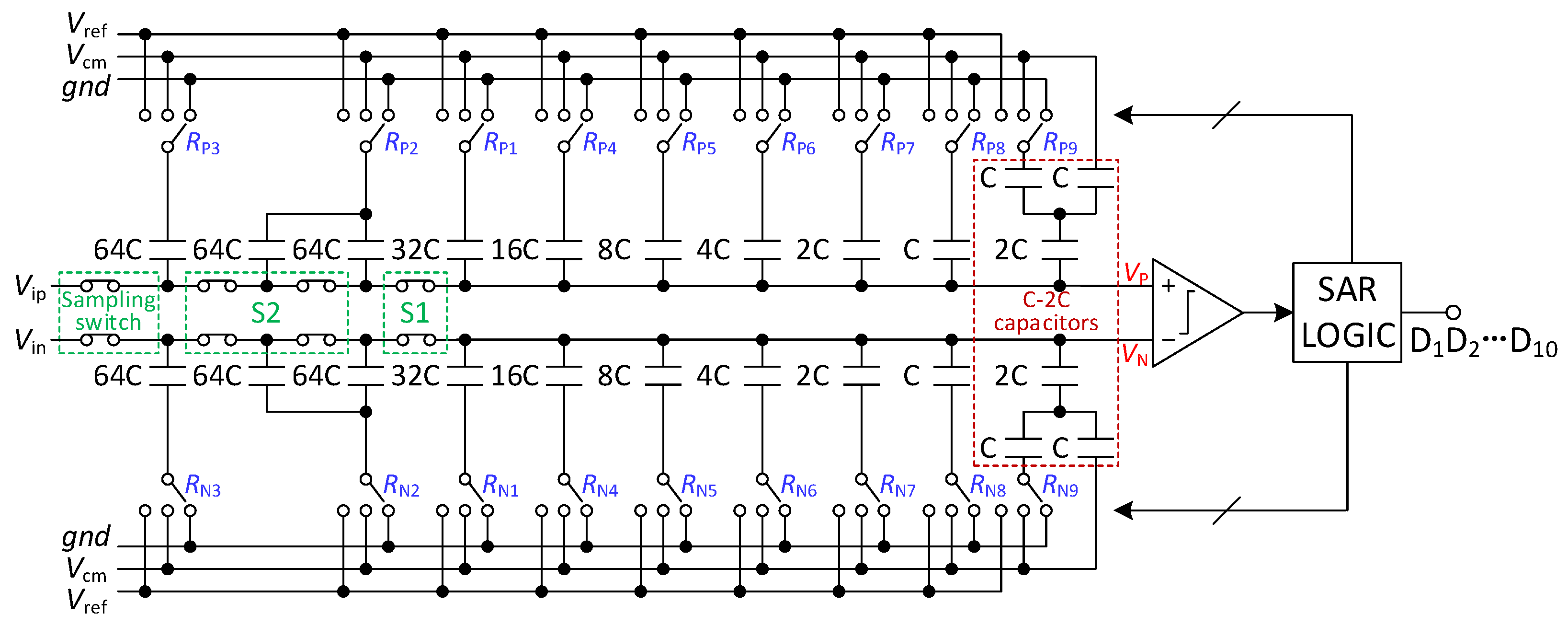
Figure 1. Architecture of 8–10-bit resolution-reconfigurable SAR ADC.
Micromachines 13 01909 g001
Figure 2. Proposed 8-bit mode switching scheme.
Micromachines 13 01909 g002
Figure 3. Proposed 9-bit mode switching scheme.
Micromachines 13 01909 g003
Figure 4. The 1st to 4th comparison diagram of the proposed 10-bit mode switching scheme.
Micromachines 13 01909 g004
Figure 5. The 5th comparison diagram of the proposed 10-bit mode switching scheme.
Micromachines 13 01909 g005
Figure 6. Switching energy against output codes: (a) 8-bit; (b) 9-bit; (c) 10-bit. The black [12], red [9], blue [10], green [11] and magenta curves in the three figures are switching energy.
Micromachines 13 01909 g006aMicromachines 13 01909 g006b
Figure 7. DNL and INL versus output code of the proposed switching scheme: (a) 8-bit mode; (b) 9-bit mode; (c) 10-bit mode.
Micromachines 13 01909 g007aMicromachines 13 01909 g007b
Figure 8. Voltage bootstrap sampling circuit.
Micromachines 13 01909 g008
Figure 9. Transient simulation of sampling switch.
Micromachines 13 01909 g009
Figure 10. FFT of sampling switch.
Micromachines 13 01909 g010
Figure 11. Two-stage fully dynamic comparator.
Micromachines 13 01909 g011
Figure 12. Transient simulation of comparator.
Micromachines 13 01909 g012
Figure 13. Monte Carlo simulation of the offset voltage for 1000 points.
Micromachines 13 01909 g013
Figure 14. SAR based on dynamic logic.
Micromachines 13 01909 g014
Figure 15. SAR control logic with bit control circuit: (a) 8-bit mode; (b) 9-bit mode; (c) 10-bit mode.
Micromachines 13 01909 g015aMicromachines 13 01909 g015b
Figure 16. Layout of the ADC.
Micromachines 13 01909 g016
Figure 17. FFT of ADC: (a) 8-bit mode; (b) 9-bit mode; (c) 10-bit mode.
Micromachines 13 01909 g017aMicromachines 13 01909 g017b
Figure 18. SNDR/SFDR with various input frequencies: (a) 8-bit mode; (b) 9-bit mode; (c) 10-bit mode.
Micromachines 13 01909 g018aMicromachines 13 01909 g018b
Figure 19. SNDR/SFDR with various sampling frequencies: (a) 8-bit mode; (b) 9-bit mode; (c) 10-bit mode.
Micromachines 13 01909 g019aMicromachines 13 01909 g019b
Figure 20. Power breakdown of the ADC: (a) 8-bit mode; (b) 9-bit mode; (c) 10-bit mode.
Micromachines 13 01909 g020aMicromachines 13 01909 g020b
Table 1. The frequency range of various biomedical signals.
Biomedical SignalsFrequency Range
Electroencephalogram (EEG)1–150 Hz
Electromyogram (EMG)25–1 kHz
Electrocardiogram (ECG)0.5–250 Hz
Local Field Potential (LFP)0.5–200 Hz
Action Potential (AP)100–7 kHz
Table 2. Resolutions of ADC are adjusted by S1 and S2.
ResolutionPhase
SamplingComparison
1st2nd3rd4th
8-bit modeS1:closeS1:openS1:openS1:openS1:open
S2:closeS2:openS2:openS2:openS2:open
9-bit modeS1:closeS1:openS1:openS1:closeS1:close
S2:closeS2:openS2:openS2:openS2:open
10-bit modeS1:closeS1:openS1:openS1:closeS1:close
S2:closeS2:openS2:openS2:openS2:close
Table 3. RP2 and RN2 for each phase of 9-bit and 10-bit mode.
D1D2Phase
SamplingComparison
1st2nd3rd
00RP2 = VcmRP2 = VcmRP2 = VcmRP2 = Vref
RN2 = VcmRN2 = VcmRN2 = VcmRN2 = gnd
01RP2 = VcmRP2 = VcmRP2 = VcmRP2 = Vcm
RN2 = VcmRN2 = VcmRN2 = VcmRN2 = Vcm
10RP2 = VcmRP2 = VcmRP2 = VcmRP2 = Vcm
RN2 = VcmRN2 = VcmRN2 = VcmRN2 = Vcm
11RP2 = VcmRP2 = VcmRP2 = VcmRP2 = gnd
RN2 = VcmRN2 = VcmRN2 = VcmRN2 = Vref
Table 4. RP3 and RN3 for each phase of 10-bit mode.
D1D3Phase
SamplingComparison
1st2nd3rd4th
00RP3 = VcmRP3 = VcmRP3 = VcmRP3 = VcmRP3 = Vref
RN3 = VcmRN3 = VcmRN3 = VcmRN3 = VcmRN3 = gnd
01RP3 = VcmRP3 = VcmRP3 = VcmRP3 = VcmRP3 = Vcm
RN3 = VcmRN3 = VcmRN3 = VcmRN3 = VcmRN3 = Vcm
10RP3 = VcmRP3 = VcmRP3 = VcmRP3 = VcmRP3 = Vcm
RN3 = VcmRN3 = VcmRN3 = VcmRN3 = VcmRN3 = Vcm
11RP3 = VcmRP3 = VcmRP3 = VcmRP3 = VcmRP3 = gnd
RN3 = VcmRN3 = VcmRN3 = VcmRN3 = VcmRN3 = Vref
Table 5. Comparison of several switching schemes for SAR ADC.
Switching Scheme Average   Switching   Energy   ( C V r e f 2 ) Energy Saving
8-Bit9-Bit10-Bit8-Bit9-Bit10-Bit
Conventional [12]339.3680.71363.3ReferenceReferenceReference
Split capacitor [9]212.3425.7852.337.4%37.4%37.4%
Set-and-down [10]63.5127.5255.581.3%81.3%81.3%
Vcm-based [11]42.284.8170.287.5%87.5%87.5%
Proposed21.226.537.193.8%96.1%97.3%
Table 6. The resolution settings of SAR logic.
MO1MO2Bit Mode
108-bit mode
019-bit mode
0010-bit mode
Table 7. Performance comparison.
Article Title[16][17][18] *[19]This Work *
Technology (nm)18018018065180180180
Supply Voltage (V)0.91.01.81.21.81.81.8
Resolution (bit)91010108910
Sampling Rate (KS/s)1001002525100100100
Power (μW)1.331.722.830.840.810.911.01
ENOB (bit)8.029.489.779.597.488.669.70
FoM (fJ/conv.-step)51.324.112943.6045.3722.512.1
* Simulated results.
Publisher’s Note: MDPI stays neutral with regard to jurisdictional claims in published maps and institutional affiliations.