Article

Atmosphere Effect in Post-Annealing Treatments for Amorphous InGaZnO Thin-Film Transistors with SiOx Passivation Layers

Department of Electronic Engineering, Shanghai Jiao Tong University, Shanghai 200240, China
*
Author to whom correspondence should be addressed.
Micromachines 2021, 12(12), 1551; https://doi.org/10.3390/mi12121551
Submission received: 1 December 2021 / Accepted: 9 December 2021 / Published: 12 December 2021
(This article belongs to the Special Issue Recent Advances in Thin Film Electronic Devices)

Abstract

:
We investigated the electrical performance and positive bias stress (PBS) stability of the amorphous InGaZnO thin-film transistors (a-IGZO TFTs) with SiOx passivation layers after the post-annealing treatments in different atmospheres (air, N2, O2 and vacuum). Both the chamber atmospheres and the device passivation layers proved important for the post-annealing effects on a-IGZO TFTs. For the heat treatments in O2 or air, the larger threshold voltage (VTH) and off current (IOFF), smaller field-effect mobility (μFE), and slightly better PBS stability of a-IGZO TFTs were obtained. The X-ray photoemission spectroscopy (XPS) and secondary ion mass spectroscopy (SIMS) measurement results indicated that the oxygen atoms from the ambience led to less oxygen vacancies (VO) and more oxygen-related defects in a-IGZO after the heat treatments in O2 or air. For the annealing processes in vacuum or N2, the electrical performance of the a-IGZO TFTs showed nearly no change, but their PBS stability evidently improved. After 4500 seconds’ stressing at 40 V, the VTH shift decreased to nearly 1 V. In this situation, the SiOx passivation layers were assumed to effectively prevent the oxygen diffusion, keep the VO concentration unchanged and refuse the oxygen-related defects into the a-IGZO films.

1. Introduction

Amorphous InGaZnO thin-film transistors (a-IGZO TFTs) have been regarded as among the most promising active-matrix devices for next-generation flat panel displays (FPDs) due to their high mobility, good uniformity and low fabrication temperature [1,2,3,4,5]. For mass productions of a-IGZO TFTs, either etching-stopper (ES) or back-channel-etching (BCE) structures are used. Although the better electrical performance and stability are obtained for ES-structured devices, BCE is still preferred for its simpler processing and compatibility with amorphous silicon (a-Si) TFT productions [6,7,8,9]. Hence, researchers have been taking many measures to improve the electrical performance and stability of BCE-structured a-IGZO TFTs, among which post-annealing treatments seem extremely useful [10,11]. Some studies pointed out that the annealing effect was closely associated with the oxygen vacancy (VO), one of the most important defects in a-IGZO films [12,13]. Assuming VO was sensitive to annealing atmospheres, as some researchers obtained higher performances and stabler properties of a-IGZO TFTs by choosing appropriate annealing atmospheres (e.g., oxygen, nitrogen, vacuum, and so on) [14,15,16,17]. However, all of these studies were limited to the unpassivated devices whereas the TFT devices are always passivated in mass production. Since passivation layers might exhibit different effects under different annealing atmospheres, it might be meaningful to investigate the atmosphere effect in post-annealing treatments for the a-IGZO TFTs with passivation layers.
In this study, the electrical performance and positive bias stress (PBS) stability of the a-IGZO TFTs with SiOx passivation layers under various post-annealing atmospheres (air, O2, N2 and vacuum) were comparatively investigated, whose physical essence was deeply analyzed with the help of X-ray photoemission spectroscopy (XPS) and secondary ion mass spectroscopy (SIMS). We found that both the chamber atmospheres and the device passivation layers played important roles in the post-annealing treatments for a-IGZO TFTs. A qualitative model was also built to explain the experimental results.

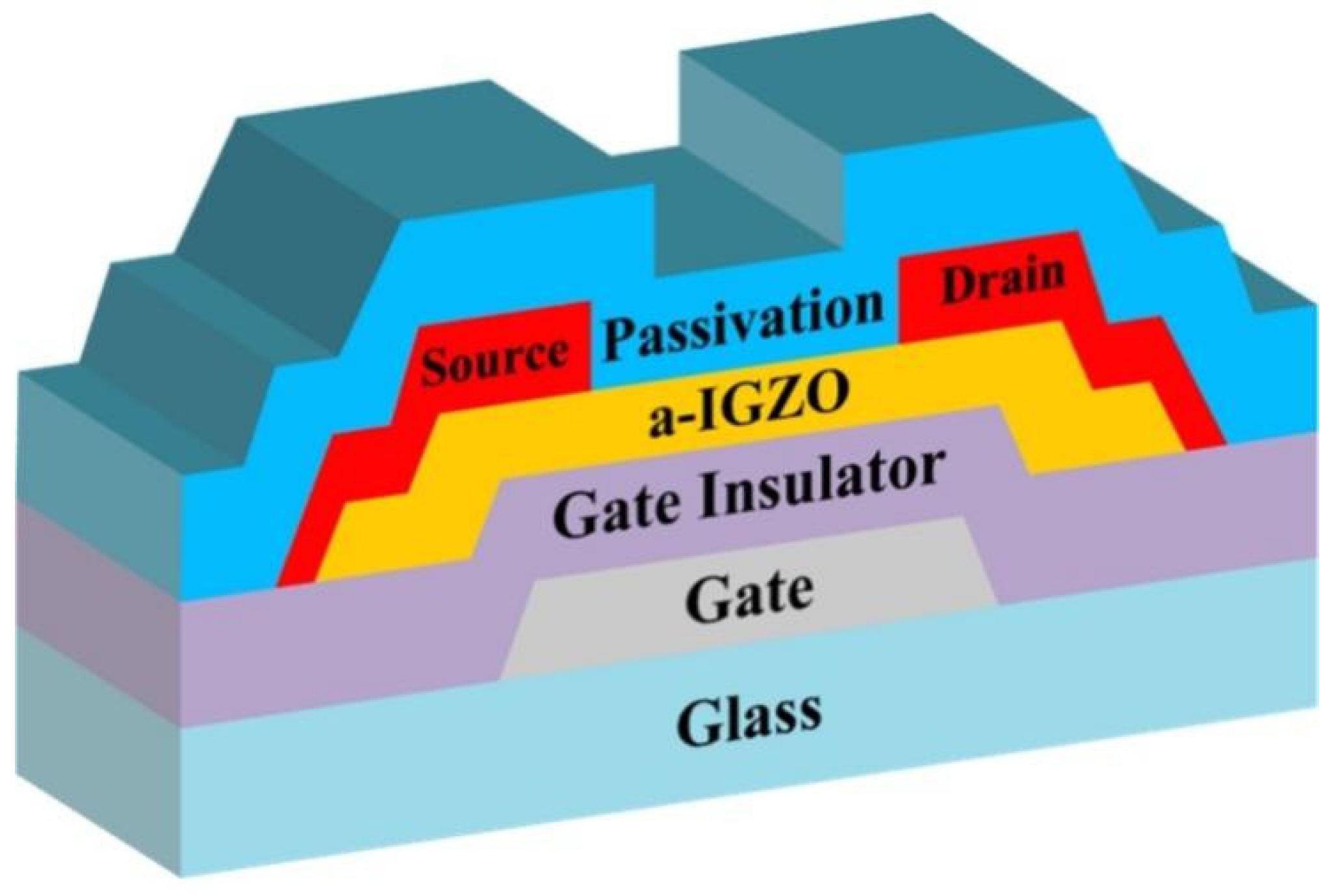
2. Materials and Methods

Figure 1 shows the schematic cross-section of the BCE-structured a-IGZO TFTs used in this study. Firstly, the gate electrodes (150 nm-thick aluminum and 23 nm-thick molybdenum films) were deposited on the glass substrates by sputtering. Then, 350 nm-thick SiNx and 50 nm-thick SiOx films were prepared as gate insulators (GIs) by plasma-enhanced chemical vapor deposition (PECVD). The 60 nm-thick channel layers were deposited by RF sputtering at room temperature (RT) using an IGZO target, where the atoms ratio of In:Ga:Zn was 1:1:1. After patterning the channel layers, a pre-annealing treatment (300 °C/1 h/air) was employed in a furnace, which could increase the film density/uniformity and reduce the defects in the a-IGZO films. The 30 nm-thick molybdenum and 150 nm-thick aluminum films were then prepared and patterned as source/drain (S/D) electrodes before the 200 nm-thick SiOx films were deposited as passivation layers by PECVD. Finally, the samples were annealed at 300 °C for 1 h in different atmospheres (air, O2, N2 and vacuum) using a rapid thermal processing (RTP) oven, where the gas flows of O2 (or N2) were set to 1 L/min and the vacuum pressure was kept at 6.5 × 10⁻³ Pa. It is worth noting that all the films were patterned by standard lithography and etching processes. The typical channel width/length of the a-IGZO TFTs was 12/6 μm.
The electrical performance and PBS stability of the a-IGZO TFTs were measured by a Keithley 2636 analyzer. The transfer curves were obtained when VGS was scanned from −20 V to 40 V at a step of 0.5 V and VDS was set to 10 V. During the PBS tests, the transfer curves were instantly measured following each 1500 s’ stressing (VGS = +40 V). All the above tests were performed in a dark chamber at RT. An XPS analyzer (AXIS Ultra DLD) was used to characterize the chemical bonding states of the a-IGZO films (without or with passivation layers) annealed under different atmospheres. Here, an X-ray source with the aluminum anode was used to bombard the film surface and obtain the energy spectrum of different elements. The binding energy of all elements were calibrated using the C1s peak at 284.8 eV. A SIMS measurement system (TOF SIMS 5 produced by ION-TOF GmbH) with a Cs+ primary ion source was applied to measure the depth profiles of different elements.

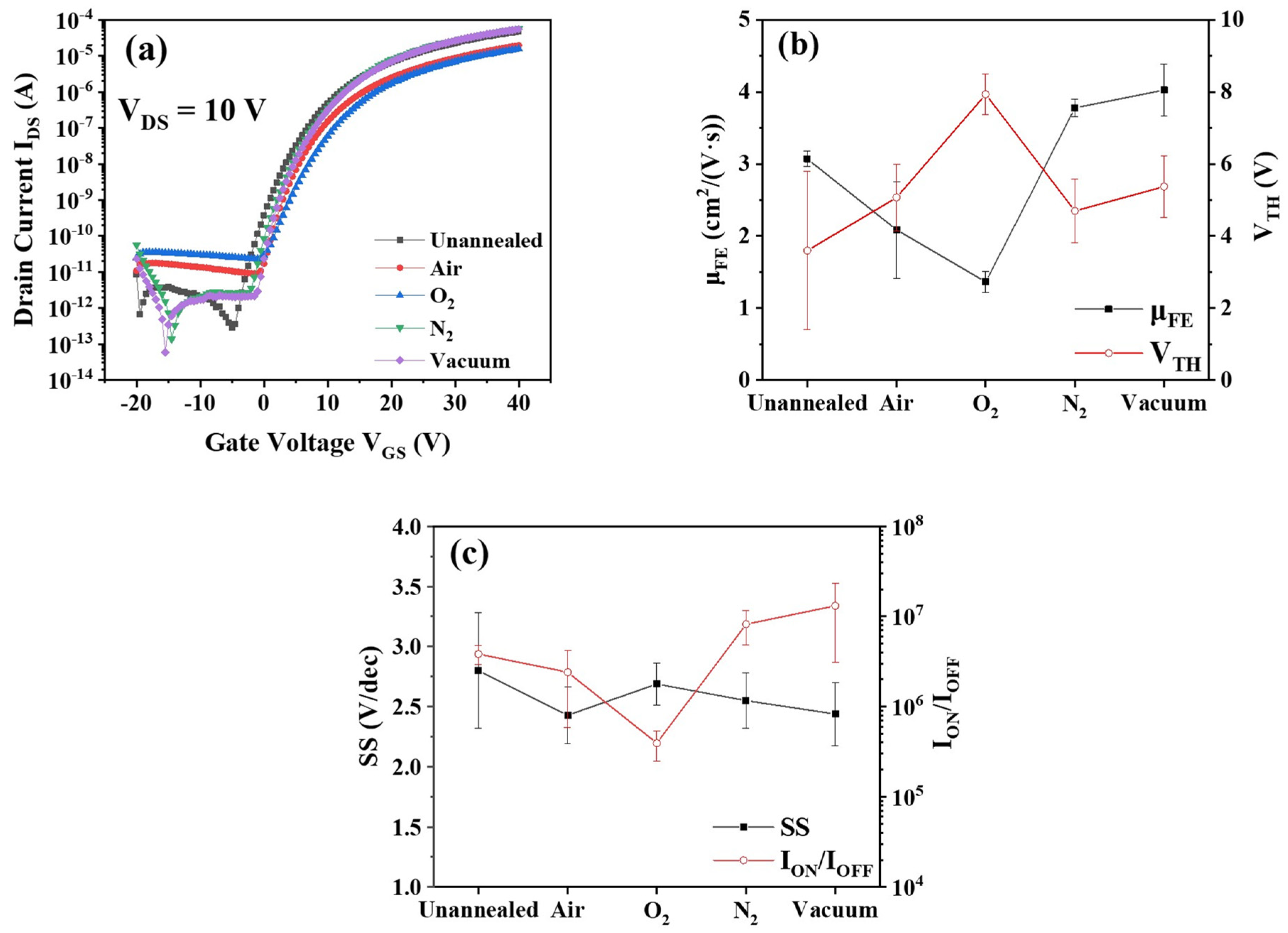
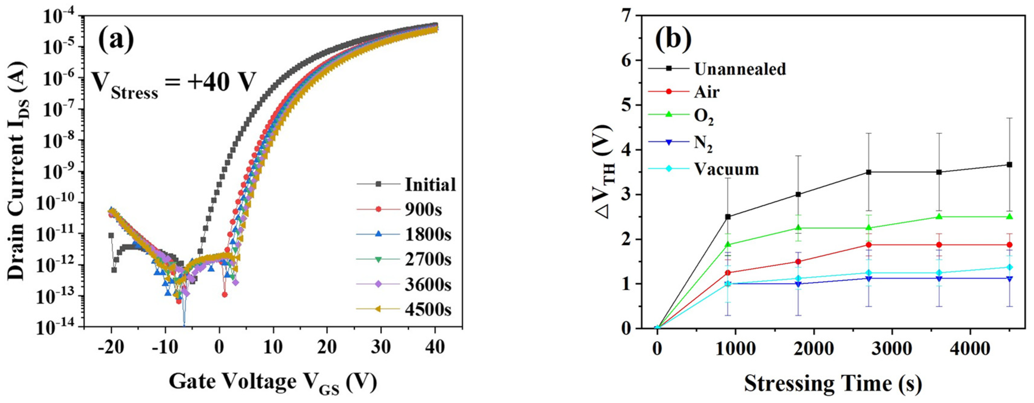
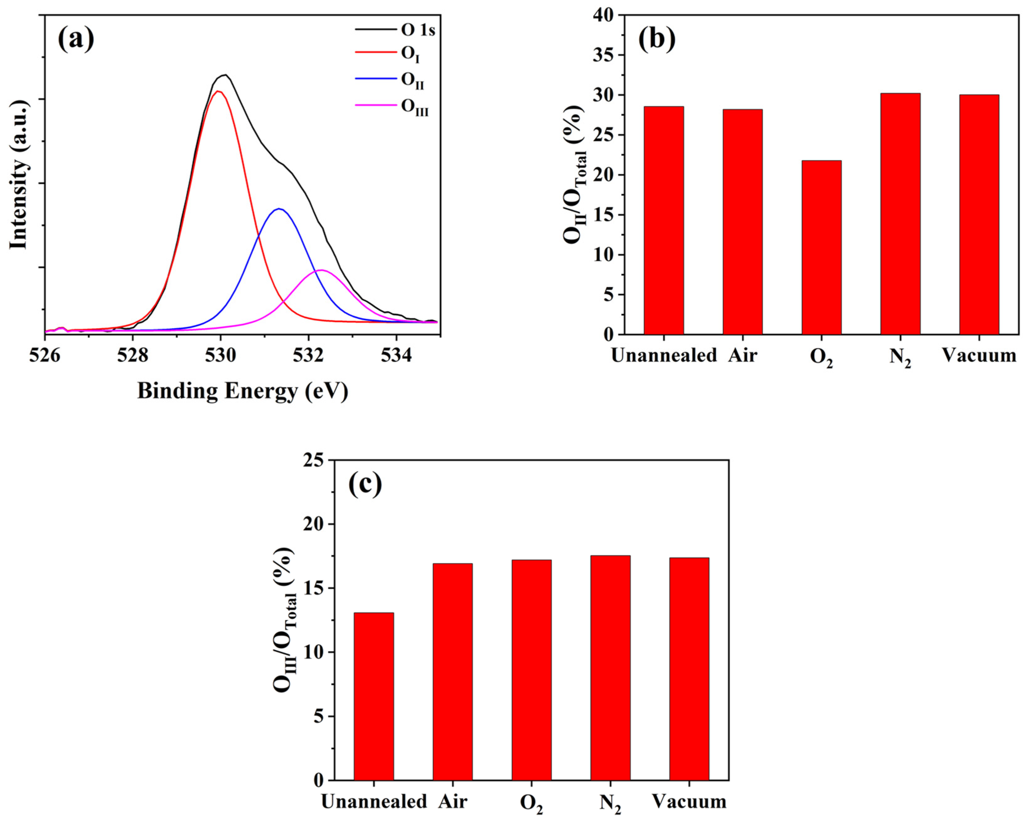
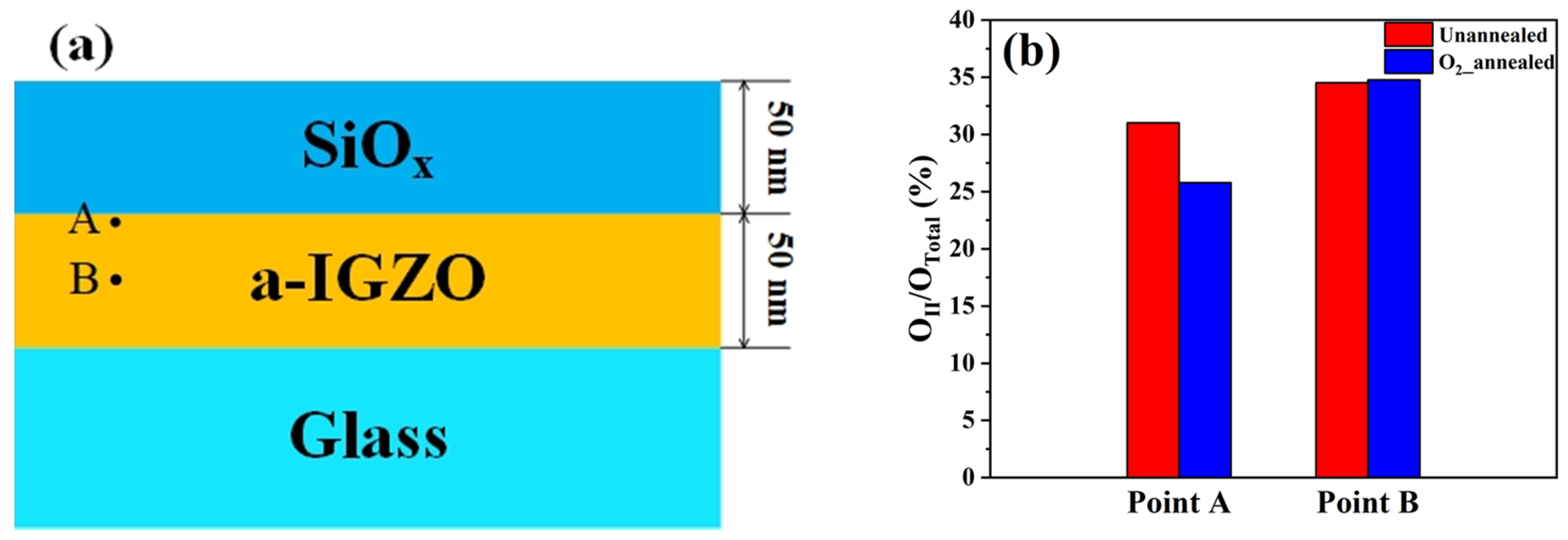
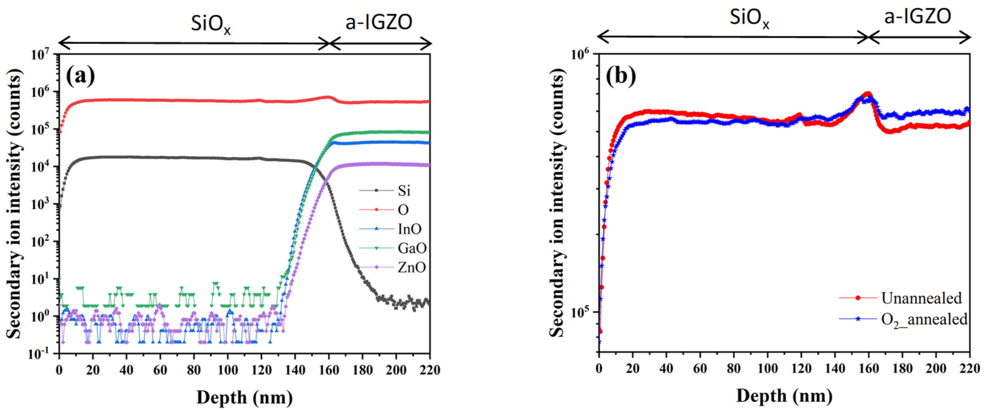
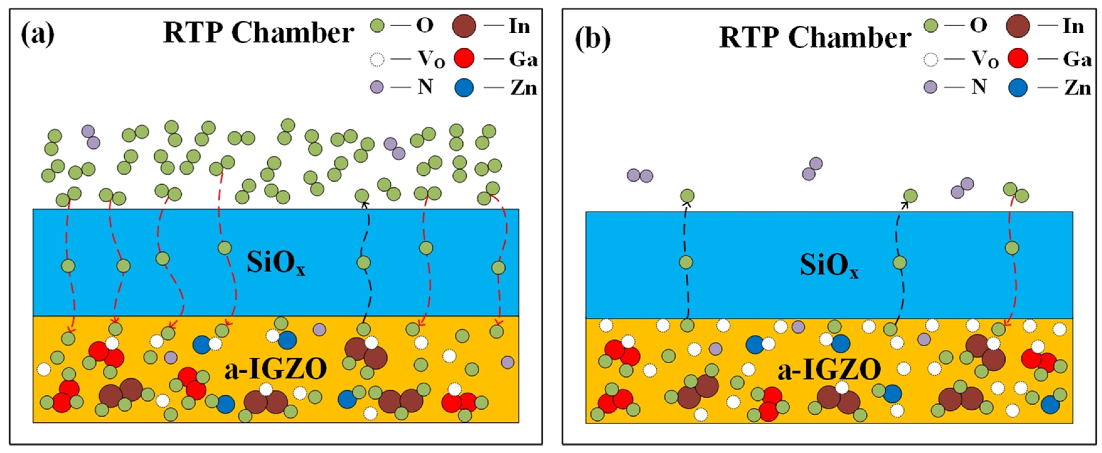
3. Results and Discussion

Figure 2a shows the transfer curves of the a-IGZO TFTs annealed under different atmospheres, where the unannealed device was considered the reference sample. The corresponding performance parameters including threshold voltage (VTH), field-effect mobility (μFE), sub-threshold swing (SS) and on–off current ratio (ION/IOFF) were extracted from the transfer curves according to Ref. [18]. Here, 6–12 devices were measured and statistically analyzed. As shown in Figure 2b, the average mobilities of the devices annealed under different atmospheres (unannealed, air, O2, N2 and vacuum) were 3.07, 2.08, 1.37, 3.78 and 4.03 cm2/(V·s), respectively. One may notice that the annealing in O2 or air obviously degraded the device mobility, whereas the annealing in N2 or vacuum slightly improved μFE. In addition, the corresponding VTH values were 3.6, 5.1, 8.0, 4.7 and 5.4 V, the SS values were 2.8, 2.4, 2.7, 2.6 and 2.4 V/dec, and the on–off current ratios were 3.8 × 10⁶, 2.4 × 10⁶, 3.9 × 10⁵, 8.2 × 10⁶ and 1.3 × 10⁷, respectively (see Figure 2b,c). Compared with the unannealed sample, one may observe from Figure 2b that the post-annealing in O2 evidently increased the threshold voltages of a-IGZO TFTs, while the annealing treatments in N2 or vacuum showed nearly no influence on the VTH values. As shown in Figure 2c, the SS values of a-IGZO TFTs remained almost the same under various post-annealing atmospheres. The post-annealing treatments resulted in sufficiently large on/off current ratios (>106) except that in O2, as shown in Figure 2c.
The bias stress effect plays an important role in the actual applications of TFT devices [2,19]. Accordingly, we measured the PBS stability of the a-IGZO TFTs with SiOx passivation under various annealing atmospheres (unannealed, air, O2, N2 and vacuum). Figure 3a shows the transfer curve evolution of the unannealed a-IGZO TFTs during PBS tests. With the stressing time elapsed, the transfer curves of the devices shifted positively. In order to quantitatively describe this unstable property, we defined a useful term ΔVTH (the VTH difference between the after-stressing state and the initial state) in this study. It is worth noting that each ΔVTH value was averaged over 3–6 devices. After 4500 s’ stressing, ΔVTH of the unannealed device became 3.67 V. All the post-annealed devices exhibited better bias stress stability than the unannealed sample. It is interesting that the ΔVTH value distinctively depended on the post-annealing atmosphere. As shown in Figure 3b, ΔVTH decreased to 1.88 V, 2.50 V, 1.13 V and 1.38 V for the devices annealed in air, O2, N2 and vacuum, respectively. It is worth noting that the post-annealing treatments in N2 and vacuum showed much larger improvements than those in O2 and air.
In order to determine the related physical mechanisms, we used the XPS technique to analyze the a-IGZO films (without or with passivation layers) annealed under various atmospheres. Firstly, we deposited 60 nm-thick a-IGZO films on glass substrates, annealed them under different atmospheres, and applied them to XPS measurements. Although these unpassivated films were different from the real situation in the TFT devices (see Figure 1), they could more evidently exhibit the influences of the annealing atmospheres on the back surfaces of the a-IGZO films. Figure 4a shows the deconvolution diagram of the O1s spectrum of the unannealed sample. The O1s peak can be deconvoluted into three sub-peaks using Gaussian fitting method which are approximately centered at 529.5 eV (OI), 530.9 eV (OII) and 532.0 eV (OIII), respectively. The OI peak represents the oxygen bonds with metal, the OII peak is bound up with VO, and the OIII peak is related to the hydrated oxides defects [20,21]. Figure 4b,c show the peak area ratios of the OII and OIII over the total area of O1s peak (OTotal = OI + OII + OIII). The area ratio OII/OTotal of the a-IGZO films annealed under various atmospheres (unannealed, air, O2, N2 and vacuum) were 28.56%, 28.19%, 21.78%, 30.20% and 30.02%, respectively. One may observe that the post-annealing in O2 largely decreased the area ratio OII/OTotal, whereas the heat treatments in air/N2/vacuum showed little effect in this regard. On the other side, the area ratio OIII/OTotal of the a-IGZO films under different atmospheres (unannealed, air, O2, N2 and vacuum) were 13.08%, 16.91%, 17.19%, 17.53% and 17.37%, respectively. It is obvious that all the post-annealing treatments increased the area ratio OIII/OTotal.
As shown in Figure 4b, only O2_annealing among five treatments evidently changed VO in a-IGZO films, which are in need of much further study. Most importantly, could passivation layers prevent this effect? Attempting to address this question, we used XPS depth profiling technique to analyze the chemical bonding states in the a-IGZO films passivated by 50 nm-thick SiOx [22]. As shown in Figure 5a, point A was exactly under the interface between the a-IGZO and SiOx, whereas point B was in the middle of a-IGZO films. The characterization results of the unannealed samples and the O2_annealed samples are shown in Figure 5b. At point A, the area ratio OII/OTotal decreased from 31.0% to 25.8% by the O2_annealing treatment, which was quite similar to the case of the unpassivated a-IGZO films (see Figure 4b). At point B, however, there was nearly no difference in the area ratio OII/OTotal between the unannealed (34.5%) and O2_annealed (34.8%) samples. These results indicated that the oxygen atoms might also diffuse into the a-IGZO back surfaces and hence combine with VO even if the SiOx passivation layer was applied during the O2_annealing treatments. Although the thickness of SiOx used here (50 nm) was thinner than that of the passivation layer (200 nm) in the a-IGZO TFTs, we assume that this conclusion was also applied to the real devices.
In order to further ascertain the role of the ambient oxygen atoms during the thermal annealing treatments, we comparatively measured the SIMS profiles of the unannealed sample and O2_annealed sample, both of which consisted of 60 nm-thick a-IGZO and 160 nm-thick SiOx films. Here, the SIMS depth profiling technique was used to analyze the distribution of different elements in the unannealed and O2-annealed samples [23]. Figure 6a shows the depth dependence of the second ion intensity for the unannealed sample. One can observe that there were abrupt changes in Si, InO, GaO and ZnO at the depth of approximately 160 nm, which was close to the interfacial surface between SiOx and a-IGZO. The O2_annealing brought nearly the same SIMS picture as that of the unannealed sample except the data about oxygen ions. As shown in Figure 6b, the secondary ion intensity of oxygen remained almost unchanged within the SiOx films by the O2_annealing, implying that the entering oxygen atoms from the ambience during the annealing treatment in O2 were too few to be detected by SIMS. Therefore, we reasonably assume that the oxygen atoms entering the a-IGZO also could not be detected by SIMS. However, as shown in Figure 6b, the secondary ion intensity of the oxygen apparently increased for the O2_annealed sample. We assume that the microstructure of the a-IGZO evidently changed during the annealing treatment in O2, which might be due to the entering oxygen atoms from the ambience although their concentration was quite small. This change also implied that the O2_annealing might bring some oxygen-related-defects such as interstitial oxygen in the a-IGZO films [24,25].
It is well known that a-IGZO films are very sensitive to ambient atmospheres, especially oxygen and water [26,27]. For mass production, passivation layers are always used to isolate a-IGZO TFTs from the ambience. However, post-annealing treatments at high temperatures accelerate the interaction between the a-IGZO and outside world. This interaction is a dynamic process during annealing treatments. Here, we limit our discussion to the interactions between oxygen atoms because they are dominant in the electrical performance and stable properties of a-IGZO TFTs. Figure 7a shows the schematic diagram of the dynamic process during the annealing treatments at 300 °C in O2 (or air) atmospheres. In this situation, the oxygen atoms were full of the RTP chamber, so the oxygen diffusion from the chamber into the a-IGZO films should prevail that from the device channel layers into the ambience. It was reported that oxygen atoms could pass through dielectric films due to thermal diffusion at high temperatures [28,29]. Importantly, these newcomers (oxygen atoms) combined with oxygen vacancies and effectively decreased the VO concentration in a-IGZO films, which was confirmed by the XPS measurement results (see Figure 4b and Figure 5b). This drop in the VO concentration accordingly resulted in the larger VTH values for the corresponding TFT devices, as shown in Figure 2b. It is worth noting that this effect was evidently weakened for the annealing treatments in air due to the existence of much more nitrogen atoms in the RTP chamber. Furthermore, the entering oxygen atoms also brought some oxygen-related-defects (see the discussion about the SIMS measurement results), and led to smaller μFE and larger IOFF (as shown in Figure 2). Generally, heat treatments could improve the bias stress stability of a-IGZO TFTs due to the drops in the bulk defects and interface traps [30,31,32]; however, these oxygen-related-defects degraded this improvement effect. Specifically, the oxygen-related defects might make the VO formation easier during positive bias stressing [33], which resulted in more unstable properties of a-IGZO TFTs. Thus, the PBS stability improvements for the a-IGZO TFTs annealed in O2 and air were not so evident, as shown in Figure 3b.
Figure 7b shows the dynamic process during the post-annealing at 300 °C in vacuum (or N2). In this situation, there were few oxygen atoms in the RTP chamber, so the oxygen diffusion from the a-IGZO film to the ambience was assumed to be dominant. If so, the VO concentration would have become larger. However, this rise in the VO concentration was not apparent due to the XPS measurement data. As shown in Figure 4b, the annealing in N2 (or vacuum) hardly changed the area ratio OII/OTotal. We ascribe this phenomenon to the barrier effect of the SiOx passivation layers. In contrast to Figure 7a, the SiOx passivation layers effectively prevented the oxygen diffusion from the a-IGZO into the ambience during heat treatments in vacuum (or N2). Since the VO concentration changed little in this case, the electron concentration in the channel layers of the a-IGZO TFTs remained nearly unchanged, leading to VTH and μFE values similar to those of the unannealed device (see Figure 2b). As for the bias stress stability of the a-IGZO TFTs annealed in vacuum (or N2), we reasonably assume that there were no oxygen-related-defects included here, so the improvement effect over the stable properties of a-IGZO TFTs by heat treatments could be well kept [34]. As shown in Figure 3b, the annealing in vacuum (or N2) effectively improved the PBS stability of the a-IGZO TFTs with SiOx passivation layers, which should be preferred in mass productions.
Finally, we briefly discussed two interesting questions relating this study. The first one is about the function of VO and the other one is relating the choice of passivation materials. Some researchers reported the VO drop led to better device performance [35,36], which is different from the results here. We ascribe this difference to the special effects of O2_annealing treatments, i.e., they not only decreased the VO concentration but also brought some oxygen-related-defects [24,25]. In this study, the SiOx was selected as passivation layers, which was found to play important roles in the post-annealing treatments under different atmospheres. We assumed that other passivation materials should bring similar tendencies but to different extents. This assumption might be supported by the other research results from our group, which indicated that the a-IGZO TFTs with SiOx and AlOx passivation layers exhibited almost the same PBS stability if the different passivation layer thicknesses were used [33]. In fact, not only the passivation material but also some treatments on passivation layers might also influence their performance during heat treatments. It is reported that the thermal stability of TFTs can be improved by using fluorinated organic passivation, where the diffusion of F during the annealing process reduced the VO, leading to better thermal stability [35]. Although the different passivation layers showed somewhat different performances, all the above reports suggested that passivation layers have similar barrier effects during post-annealing treatments.

4. Conclusions

The post-annealing atmosphere effectively influenced the electrical performance and bias stress stability of the a-IGZO TFTs with SiOx passivation layers. For the heat treatments in O2 (or air), the oxygen atoms in the ambience diffused into the a-IGZO and combined with oxygen vacancies, leading to less VO and more oxygen-related defects; this resulted in larger VTH/IOFF, smaller μFE and the slightly better PBS stability of the a-IGZO TFTs. For the post-annealing process in vacuum (or N2), the oxygen diffusion was effectively prevented by the SiOx passivation layers, and hence the VO concentration hardly changed; the electrical performance of the a-IGZO TFTs showed nearly no change, but very importantly, their PBS stability evidently improved. This qualitative model was confirmed by the XPS and SIMS measurement results.

Author Contributions

Conceptualization, W.Z., Z.F., A.S. and C.D.; investigation, W.Z.; writing, W.Z., Z.F., A.S. and C.D. All authors have read and agreed to the published version of the manuscript.

Funding

This work was supported by the Key Research Project of Jiangxi Province (Grant No. 20194ABC28005). The authors thank Chen Wang, Cong Peng and Xi Feng Li (Shanghai University) for their support in the device fabrications.

Data Availability Statement

The data presented in this study are available on request from the corresponding author.

Conflicts of Interest

The authors declare no conflict of interest.

References

  1. Nomura, K.; Ohta, H.; Takagi, A.; Kamiya, T.; Hirano, M.; Hosono, H. Room-temperature fabrication of transparent flexible thin-film transistors using amorphous oxide semiconductors. Nature 2004, 432, 488–492. [Google Scholar] [CrossRef]
  2. Kamiya, T.; Nomura, K.; Hosono, H. Present status of amorphous In–Ga–Zn–O thin-film transistors. Sci. Technol. Adv. Mater. 2010, 11, 044305. [Google Scholar] [CrossRef]
  3. Yabuta, H.; Sano, M.; Abe, K.; Aiba, T.; Den, T.; Kumomi, H.; Nomura, K.; Kamiya, T.; Hosono, H. High-mobility thin-film transistor with amorphous InGaZnO4 channel fabricated by room temperature rf-magnetron sputtering. Appl. Phys. Lett. 2006, 89, 112123. [Google Scholar] [CrossRef]
  4. Lee, J.; Kim, D.; Yang, D.; Hong, S.; Yoon, K.; Hong, P.; Jeong, C.; Park, H.; Kim, S.; Lim, S.; et al. 42.2: World’s largest (15-inch) XGA AMLCD panel using IGZO oxide TFT. SID Symp. Dig. Tech. Pap. 2008, 39, 625–628. [Google Scholar] [CrossRef]
  5. Jeong, J.; Jeong, J.; Choi, J.; Im, J.; Kim, S.; Yang, H.; Kang, K.; Kim, K.; Ahn, T.; Chung, H.; et al. 3.1: Distinguished Paper: 12.1-Inch WXGA AMOLED display driven by indium-gallium-zinc oxide TFTs array. SID Symp. Dig. Tech. Pap. 2008, 39, 1–4. [Google Scholar] [CrossRef]
  6. Kim, M.K.; Jeong, J.H.; Lee, H.J.; Ahn, T.K.; Shin, H.S.; Park, J.S.; Jeong, J.K.; Mo, Y.G.; Kim, H.D. High mobility bottom gate InGaZnO thin film transistors with SiOx etch stopper. Appl. Phys. Lett. 2007, 90, 212114. [Google Scholar] [CrossRef]
  7. Peng, C.; Yang, S.; Pan, C.; Li, X.; Zhang, J. Effect of two-step annealing on high stability of a-IGZO thin-film transistor. IEEE Trans. Electron Devices 2020, 67, 4262–4268. [Google Scholar] [CrossRef]
  8. Nag, M.; Bhoolokam, A.; Steudel, S.; Chasin, A.; Myny, K.; Maas, J.; Groeseneken, G.; Heremans, P. Back-channel-etch amorphous indium–gallium–zinc oxide thin-film transistors: The impact of source/drain metal etch and final passivation. Jpn. J. Appl. Phys. 2014, 53, 111401. [Google Scholar] [CrossRef]
  9. Park, Y.; Um, J.; Mativenga, M.; Jang, J. Enhanced operation of back-channel-etched a-IGZO TFTs by fluorine treatment during source/drain wet-etching. ECS J. Solid State Sci. Technol. 2017, 6, 300–303. [Google Scholar] [CrossRef]
  10. Ochi, M.; Hino, A.; Goto, H.; Hayashi, K.; Kugimiya, T. Improvement of stress stability in back channel etch-type amorphous In–Ga–Zn–O thin film transistors with post process annealing. ECS J. Solid State Sci. Technol. 2017, 6, 247–252. [Google Scholar] [CrossRef]
  11. Yu, Y.; Lv, N.; Zhang, D.; Wei, Y.; Wang, M. High-mobility amorphous InGaZnO thin-film transistors with nitrogen introduced via low-temperature annealing. IEEE Electron Device Lett. 2021, 42, 1480–1483. [Google Scholar] [CrossRef]
  12. Trinh, T.; Nguyen, V.; Ryu, K.; Jang, K.; Lee, W.; Baek, S.; Raja, J.; Yi, J. Improvement in the performance of an InGaZnO thin-film transistor by controlling interface trap densities between the insulator and active layer. Semicond. Sci. Technol. 2011, 26, 085012. [Google Scholar] [CrossRef]
  13. Jung, C.; Kim, D.; Kang, Y.; Yoon, D. Effect of heat treatment on electrical properties of amorphous oxide semiconductor In–Ga–Zn–O film as a function of oxygen flow rate. Jpn. J. Appl. Phys. 2009, 48, 08HK02. [Google Scholar] [CrossRef]
  14. Lin, C.; Yen, T.; Lin, H.; Huang, T.; Lee, Y. Effect of annealing ambient on the characteristics of a-IGZO thin film transistors. In Proceedings of the 4th IEEE International NanoElectronics Conference, Taiwan, China, 21–24 June 2011; pp. 1–2. [Google Scholar]
  15. Fuh, C.; Sze, S.; Liu, P.; Teng, L.; Chou, Y. Role of environmental and annealing conditions on the passivation–free In–Ga–Zn–O TFT. Thin Solid Films 2011, 520, 1489–1494. [Google Scholar] [CrossRef]
  16. Gutierrez-Heredia, G.; Maeng, J.; Conde, J.; Rodriguez-Lopez, O.; Voit, W.E. Effect of annealing atmosphere on IGZO thin film transistors on a deformable softening polymer substrate. Semicond. Sci. Technol. 2018, 33, 095001. [Google Scholar] [CrossRef]
  17. Huang, Y.; Yang, P.; Huang, H.; Wang, S.; Cheng, H. Effect of the annealing ambient on the electrical characteristics of the amorphous InGaZnO thin film transistors. J. Nanosci. Nanotechnol. 2012, 12, 5625–5630. [Google Scholar] [CrossRef] [PubMed]
  18. Wu, J.; Chen, Y.; Zhou, D.; Hu, Z.; Xie, H.; Dong, C. Sputtered oxides used for passivation layers of amorphous InGaZnO thin film transistors. Mater. Sci. Semicond. Process. 2015, 29, 277–282. [Google Scholar] [CrossRef]
  19. Nguyen, C.; Trinh, T.; Dao, V.; Raja, J.; Jang, K.; Le, T.; Iftiquar, S.; Yi, J. Bias-stress-induced threshold voltage shift dependence of negative charge trapping in the amorphous indium tin zinc oxide thin-film transistors. Semicond. Sci. Technol. 2013, 28, 105014. [Google Scholar] [CrossRef]
  20. Xie, H.; Xu, J.; Liu, G.; Zhang, L.; Dong, C. Development and analysis of nitrogen-doped amorphous InGaZnO thin film transistors. Mater. Sci. Semicond. Process. 2017, 64, 1–5. [Google Scholar] [CrossRef]
  21. Zhou, X.; Han, D.; Dong, J.; Li, H.; Yi, Z.; Xing, Z.; Wang, Y. The effects of post annealing process on the electrical performance and stability of Al-Zn-O thin-film transistors. IEEE Electron Device Lett. 2020, 41, 569–572. [Google Scholar] [CrossRef]
  22. Chun, M.; Um, J.; Park, M.; Chowdhury, M.; Jang, J. Effect of top gate potential on bias-stress for dual gate amorphous indium-gallium-zinc-oxide thin film transistor. AIP Adv. 2016, 6, 075217. [Google Scholar] [CrossRef] [Green Version]
  23. Nomura, K.; Kamiya, T.; Hosono, H. Effects of diffusion of hydrogen and oxygen on electrical properties of amorphous oxide semiconductor, In-Ga-Zn-O. ECS J. Solid State Sci. Technol. 2012, 2, 5–8. [Google Scholar] [CrossRef]
  24. Yang, J.; Cao, D.; Lin, D.; Liu, F. Effect of annealing ambient gases on the bias stability of amorphous SnSiO thin-film transistors. Semicond. Sci. Technol. 2020, 35, 115003. [Google Scholar] [CrossRef]
  25. Su, J.; Yang, H.; Ma, Y.; Li, R.; Jia, L.; Liu, D.; Zhang, X. Annealing atmosphere-dependent electrical characteristics and bias stability of N-doped InZnSnO thin film transistors. Mater. Sci. Semicond. Process. 2020, 113, 105040. [Google Scholar] [CrossRef]
  26. Chen, Y.; Chang, T.; Li, H.; Chen, S.; Chung, W.; Chen, Y.; Tai, Y.; Tseng, T.; Huang, F. Surface states related the bias stability of amorphous In–Ga–Zn–O thin film transistors under different ambient gasses. Thin Solid Films 2011, 520, 1432–1436. [Google Scholar] [CrossRef]
  27. Dong, C.; Xu, J.; Zhou, Y.; Zhang, Y.; Xie, H. Light-illumination stability of amorphous InGaZnO thin film transistors in oxygen and moisture ambience. Solid-State Electron. 2019, 153, 74–78. [Google Scholar] [CrossRef]
  28. Pearton, S.; Cho, H.; LaRoche, J.; Ren, F.; Wilson, R.; Lee, J. Oxygen diffusion into SiO2-capped GaN during annealing. Appl. Phys. Lett. 1999, 75, 2939–2941. [Google Scholar] [CrossRef]
  29. Nguyen, T.; Renault, O.; Aventurier, B.; Rodriguez, G.; Barnes, J.; Templier, F. Analysis of IGZO thin-film transistors by XPS and relation with electrical characteristics. J. Disp. Technol. 2013, 9, 770–774. [Google Scholar] [CrossRef]
  30. Chen, W.; Lo, S.; Kao, S.; Zan, H.; Tsai, C.; Lin, J.; Fang, C. Oxygen-dependent instability and annealing/passivation effects in amorphous In–Ga–Zn–O thin-film transistors. IEEE Electron Device Lett. 2011, 32, 1552–1554. [Google Scholar] [CrossRef]
  31. Qu, M.; Chang, C.; Meng, T.; Zhang, Q.; Liu, P.; Shieh, H. Stability study of indium tungsten oxide thin-film transistors annealed under various ambient conditions. Phys. Status Solidi 2016, 214, 1600465. [Google Scholar] [CrossRef]
  32. Nomura, K.; Kamiya, T.; Hirano, M.; Hosono, H. Origins of threshold voltage shifts in room-temperature deposited and annealed a-In–Ga–Zn–O thin-film transistors. Appl. Phys. Lett. 2009, 95, 013502. [Google Scholar] [CrossRef]
  33. Zhou, Y.; Dong, C. Influence of passivation layers on positive gate bias-stress stability of amorphous InGaZnO thin-film transistors. Micromachines 2018, 9, 603. [Google Scholar] [CrossRef] [Green Version]
  34. Lee, H.; Cho, W. Effects of vacuum rapid thermal annealing on the electrical characteristics of amorphous indium gallium zinc oxide thin films. AIP Adv. 2018, 8, 015007. [Google Scholar] [CrossRef]
  35. Park, Y.; Um, J.; Mativenga, M.; Jang, J. Thermal stability improvement of back channel etched a-IGZO TFTs by using fluorinated organic passivation. ECS J. Solid State Sci. Technol. 2018, 7, 123–126. [Google Scholar] [CrossRef]
  36. Kim, C.; Kim, E.; Lee, M.; Park, J.; Seol, M.; Bae, H.; Bang, T.; Jeon, S.; Jun, S.; Park, S.; et al. Electrothermal annealing (ETA) method to enhance the electrical performance of amorphous-oxide-semiconductor (AOS) thin-film transistors (TFTs). ACS Appl. Mater. Interfaces 2016, 8, 23820–23826. [Google Scholar] [CrossRef] [PubMed]
Figure 1. Schematic cross-section of the back-channel-etching (BCE) -structured amorphous InGaZnO thin-film transistors (a-IGZO TFTs) in this study.
Micromachines 12 01551 g001
Figure 2. (a) Transfer curves; (b) mobility/threshold voltage; and (c) sub-threshold slope/on–off current ratio of the a-IGZO TFTs with SiOx passivation layers annealed in different atmospheres.
Micromachines 12 01551 g002
Figure 3. (a) Stressing time dependence of the transfer curves of the unannealed a-IGZO TFTs with SiOx passivation layers; (b) threshold voltage shifts of the a-IGZO TFTs with SiOx passivation layers annealed under different atmospheres during PBS tests.
Micromachines 12 01551 g003
Figure 4. (a) Deconvolution diagram of the O1s peak of the unannealed a-IGZO films; the area ratios of (b) O and (c) O in the O1s peak of the a-IGZO films annealed under different atmospheres.
Micromachines 12 01551 g004
Figure 5. (a) The sample structure for the XPS depth profiling tests; (b) the area ratios of O in the O1s peak of the unannealed and O2_annealed samples.
Micromachines 12 01551 g005
Figure 6. (a) SIMS depth profiles for the unannealed sample; (b) the oxygen depth distributions for the unannealed sample and the O2_annealed sample.
Micromachines 12 01551 g006
Figure 7. Schematic diagrams of the dynamic processes during the post-annealing treatments at 300 °C in (a) O2 (or air) and (b) vacuum (or N2).
Micromachines 12 01551 g007
Publisher’s Note: MDPI stays neutral with regard to jurisdictional claims in published maps and institutional affiliations.

