
Application of Laser Treatment in MOS-TFT Active Layer Prepared by Solution Method


 , ,
, , 
Abstract
:1. Introduction
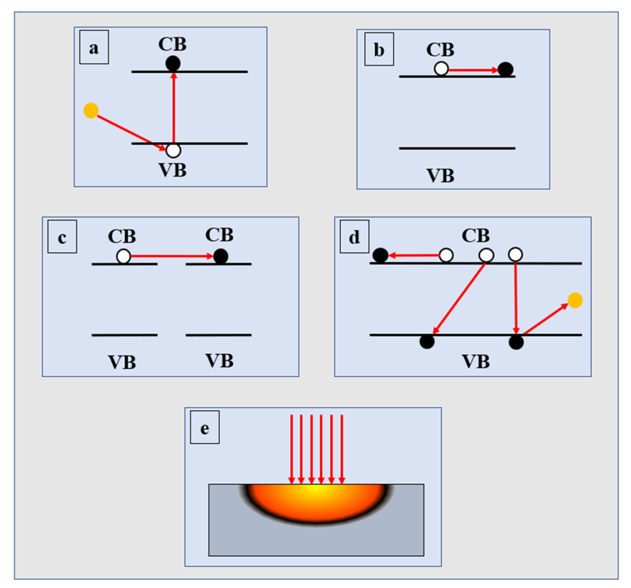
2. Mechanism of Laser Treatment
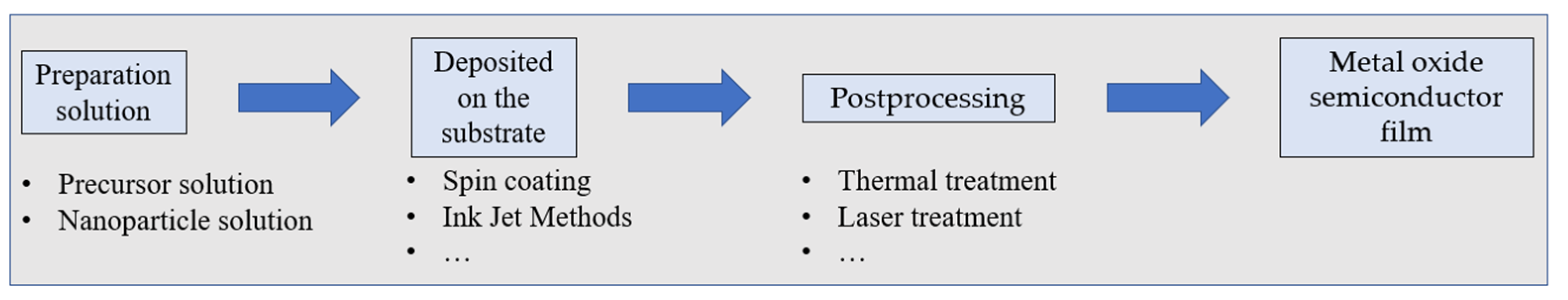
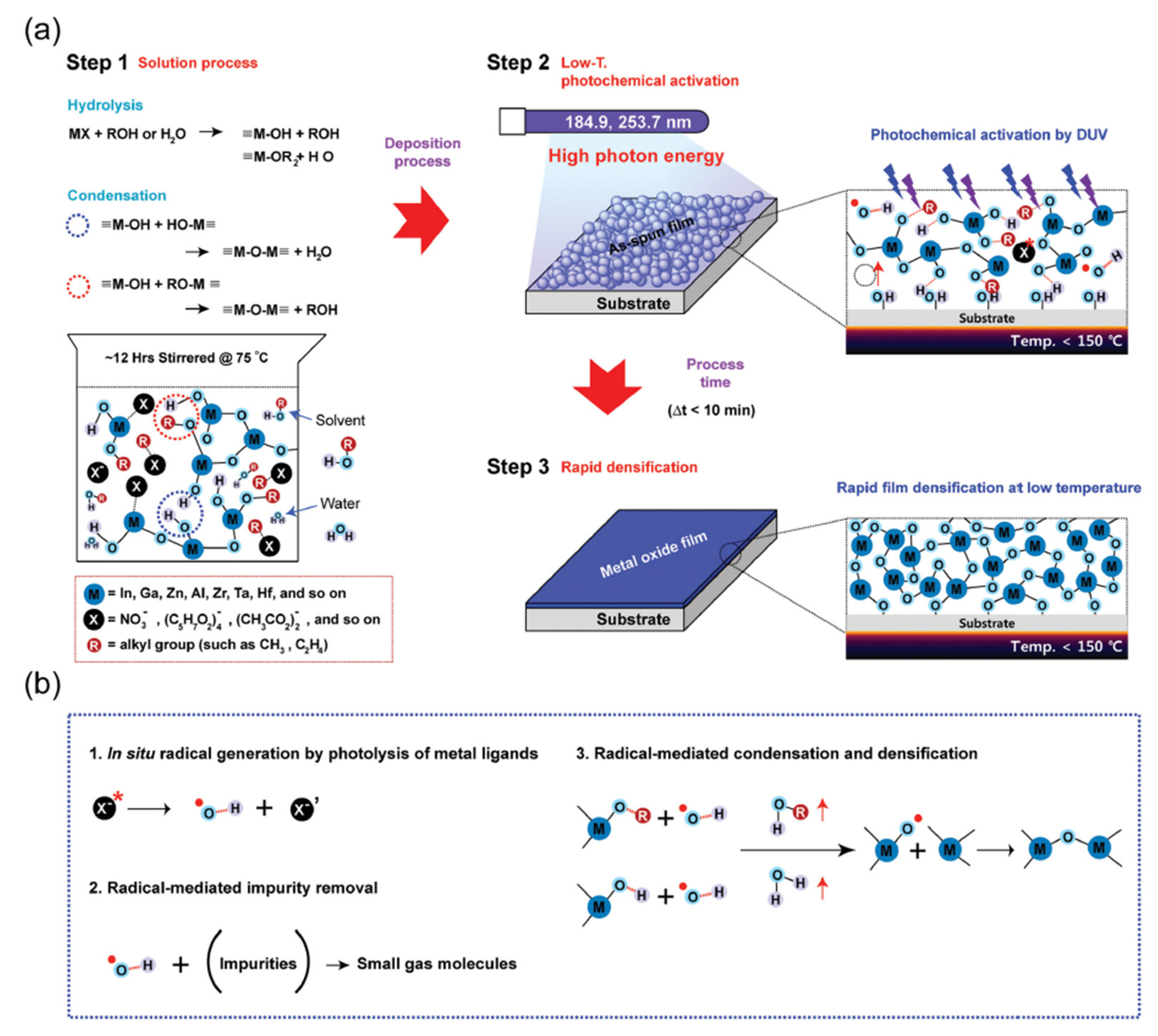
2.1. Active Layer Thin Films Prepared by Sol-Gel Method
2.2. Active Layer Thin Films Prepared by Nano-Particle Method
3. Application of Laser Treatment in MOS-TFT Performance Control
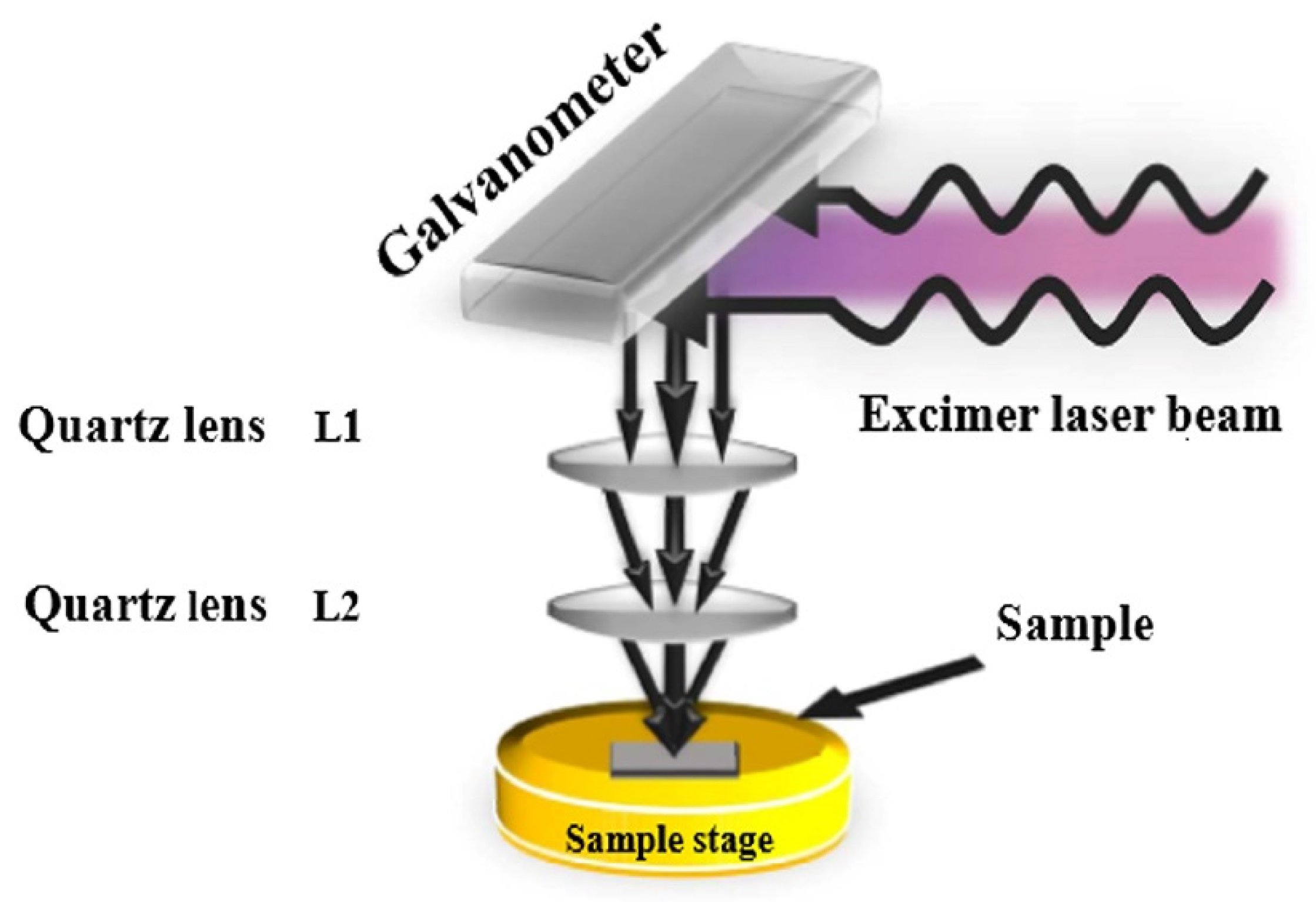
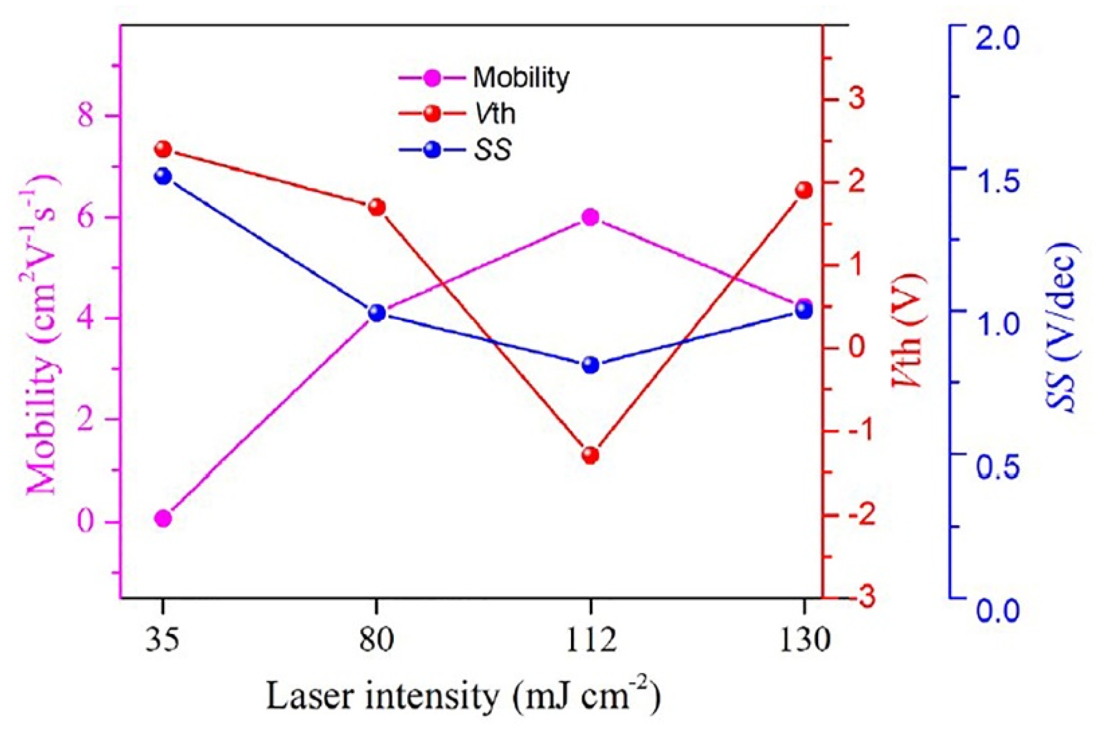
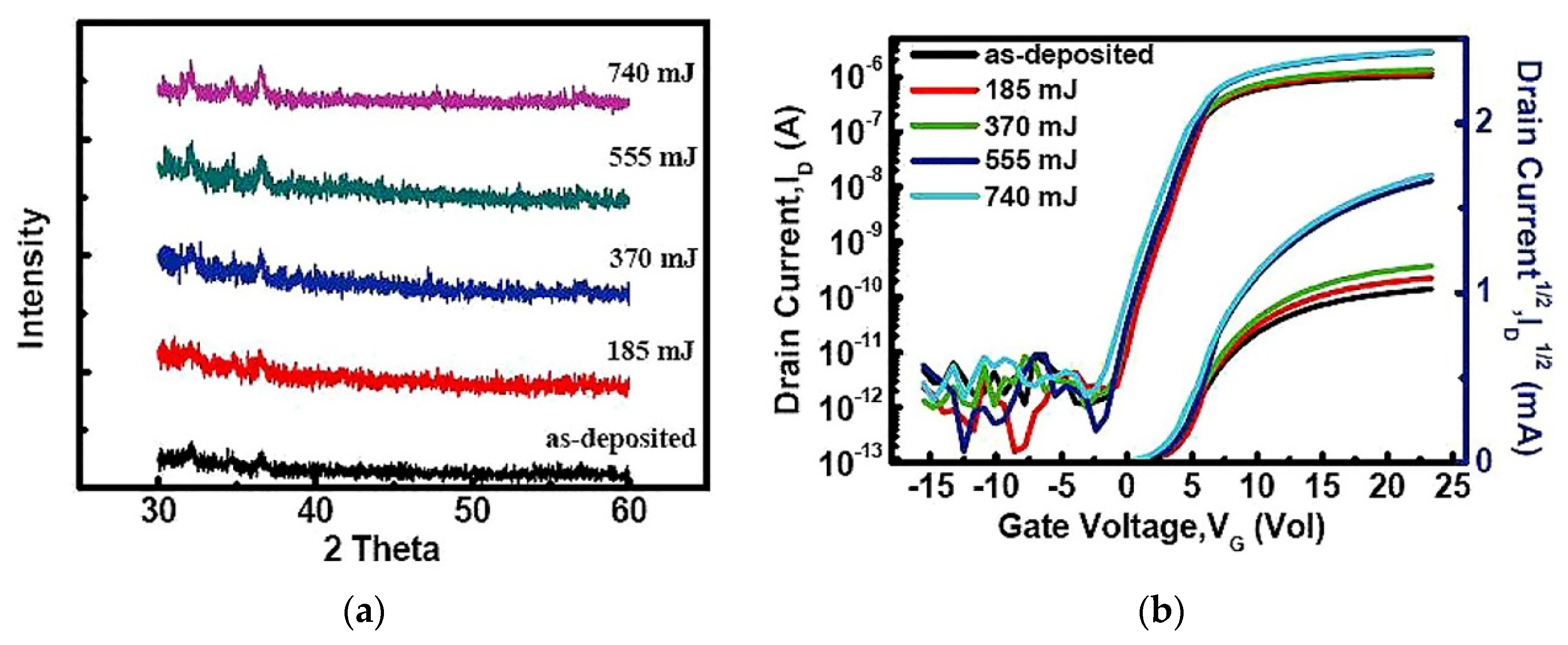
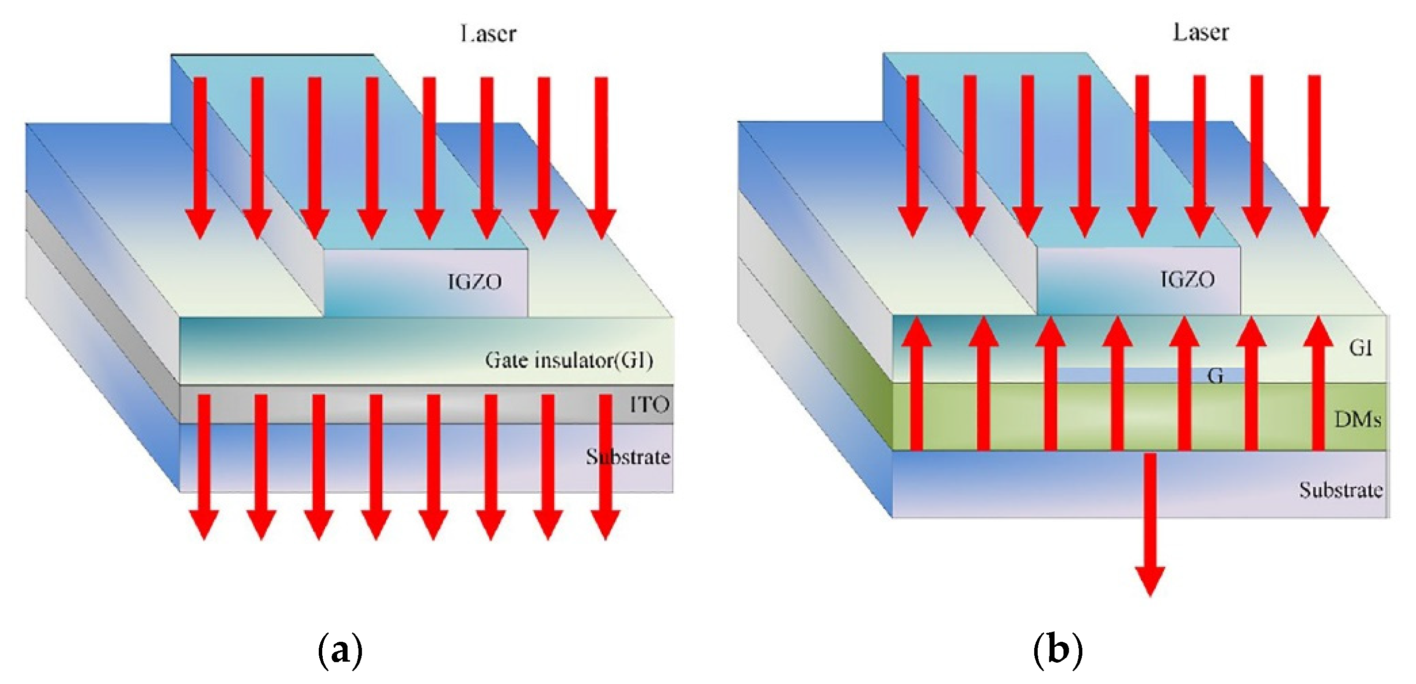
3.1. Laser Energy Density
3.2. Treatment Atmosphere
3.3. Laser Wavelength
4. Conclusions and Prospects
Author Contributions
Funding
Conflicts of Interest
References
- Yao, R.H.; Fu, X.; Li, X.Q.; Qiu, T.; Ning, H.L.; Yang, Y.X.; Lu, X.B.; Cao, X.H.; Chen, Y.; Peng, J.B. Performances of thin film transistors with Ga-doped ZnO source and drain electrodes. J. Phys. D-Appl. Phys. 2021, 54, 365101–365107. [Google Scholar] [CrossRef]
- Hu, S.; Lu, K.; Ning, H.; Yao, R.; Gong, Y.; Pan, Z.; Guo, C.; Wang, J.; Pang, C.; Gong, Z.; et al. Study of the Correlation between the Amorphous Indium-Gallium-Zinc Oxide Film Quality and the Thin-Film Transistor Performance. Nanomaterials 2021, 11, 522. [Google Scholar] [CrossRef]
- Liu, X.; Shiah, Y.-S.; Guo, D.; Ning, H.; Zhang, X.; Chen, J.; Fu, X.; Wang, Y.; Yao, R.; Peng, J. Origin of bias-stress and illumination instability in low-cost, wide-bandgap amorphous Si-doped tin oxide-based thin-film transistors. J. Phys. D-Appl. Phys. 2020, 53, 235102–235107. [Google Scholar] [CrossRef]
- Lu, K.; Yao, R.; Xu, W.; Ning, H.; Zhang, X.; Zhang, G.; Li, Y.; Zhong, J.; Yang, Y.; Peng, J. Alloy-Electrode-Assisted High-Performance Enhancement-Type Neodymium-Doped Indium-Zinc-Oxide Thin-Film Transistors on Polyimide Flexible Substrate. Research 2021, 2021. [Google Scholar] [CrossRef]
- Lu, K.; Zhang, J.; Guo, D.; Xiang, J.; Lin, Z.; Zhang, X.; Wang, T.; Ning, H.; Yao, R.; Peng, J. High-Performance and Flexible Neodymium-Doped Indium-Zinc-Oxide Thin-Film Transistor with All Copper Alloy Electrodes. IEEE Electron. Device Lett. 2020, 41, 417–420. [Google Scholar] [CrossRef]
- Sameshima, T.; Usui, S.; Sekiya, M. XeCl excimer laser annealing used in the fabrication of poly-Si TFTs. IEEE Electron. Device Lett. 1986, 1986, 276–278. [Google Scholar] [CrossRef]
- Kang, D.H.; Park, M.K.; Jang, J.; Chang, Y.J.; Oh, J.H.; Choi, J.B.; Kim, C.W. Active-matrix organic light-emitting diode using inverse-staggered poly-Si TFTs with a center-offset gated structure. J. Soc. Inf. Disp. 2010, 18, 122–127. [Google Scholar] [CrossRef]
- Kugimiya, T.; Yoneda, Y.; Kusumoto, E.; Gotoh, H.; Ochi, M.; Kawakami, N.; Sid. Single layer Al-Ni-La-Si interconnections for source and drain of LTPS-TFT LCDs using direct contacts with both ITO and poly-Si. In Proceedings of the International Symposium of the Society-for-Information-Display (SID 2008), Los Angeles, CA, USA, 18–23 May 2008. [Google Scholar]
- Nomura, K.; Ohta, H.; Takagi, A.; Kamiya, T.; Hirano, M.; Hosono, H. Room-temperature fabrication of transparent flexible thin-film transistors using amorphous oxide semiconductors. Nature 2004, 432, 488–492. [Google Scholar] [CrossRef]
- Ye, Q.; Zhang, X.; Guo, D.; Xu, W.; Ning, H.; Qiu, T.; Li, J.; Hou, D.; Yao, R.; Peng, J. Preparation of Highly Transparent (at 450–800 nm) SnO2 Homojunction by Solution Method and Its Photoresponse. Coatings 2020, 10, 399. [Google Scholar] [CrossRef] [Green Version]
- Cai, W.; Zhu, Z.; Wei, J.; Fang, Z.; Ning, H.; Zheng, Z.; Zhou, S.; Yao, R.; Peng, J.; Lu, X. A Simple Method for High-Performance, Solution-Processed, Amorphous ZrO2 Gate Insulator TFT with a High Concentration Precursor. Materials 2017, 10, 972. [Google Scholar] [CrossRef] [Green Version]
- Liang, Z.; Zhou, S.; Cai, W.; Fu, X.; Ning, H.; Chen, J.; Yuan, W.; Zhu, Z.; Yao, R.; Peng, J. Zirconium-Aluminum-Oxide Dielectric Layer with High Dielectric and Relatively Low Leakage Prepared by Spin-Coating and the Application in Thin-Film Transistor. Coatings 2020, 10, 282. [Google Scholar] [CrossRef] [Green Version]
- Ning, H.; Zhang, X.; Wang, S.; Yao, R.; Liu, X.; Hou, D.; Ye, Q.; Li, J.; Huang, J.; Cao, X.; et al. Preparation and optimization of SnOx thin film by solution method at low temperature. Superlattices Microstruct. 2020, 139, 106400–106408. [Google Scholar] [CrossRef]
- Zhu, Z.; Zhang, J.; Guo, D.; Ning, H.; Zhou, S.; Liang, Z.; Yao, R.; Wang, Y.; Lu, X.; Peng, J. Functional Metal Oxide Ink Systems for Drop-on-Demand Printed Thin-Film Transistors. Langmuir 2020, 36, 8655–8667. [Google Scholar] [CrossRef]
- Natsume, Y.; Sakata, H. Zinc oxide films prepared by sol-gel spin-coating. Thin Solid Films 2000, 372, 30–36. [Google Scholar] [CrossRef]
- Ohyama, M.; Kozuka, H.; Yoko, T. Sol-gel preparation of ZnO films with extremely preferred orientation along (002) plane from zinc acetate solution. Thin Solid Films 1997, 306, 78–85. [Google Scholar] [CrossRef]
- Sun, B.; Sirringhaus, H. Solution-processed zinc oxide field-effect transistors based on self-assembly of colloidal nanorods. Nano Lett. 2005, 5, 2408–2413. [Google Scholar] [CrossRef]
- Berber, M.; Bulto, V.; Kliss, R.; Hahn, H. Transparent nanocrystalline ZnO films prepared by spin coating. Scr. Mater. 2005, 53, 547–551. [Google Scholar] [CrossRef]
- Ismail, B.; Abaab, M.; Rezig, B. Structural and electrical properties of ZnO films prepared by screen printing technique. Thin Solid Films 2001, 383, 92–94. [Google Scholar] [CrossRef]
- Subramanian, V.; Bakhishev, T.; Redinger, D.; Volkman, S.K. Solution-Processed Zinc Oxide Transistors for Low-Cost Electronics Applications. J. Disp. Technol. 2009, 5, 525–530. [Google Scholar] [CrossRef]
- Banger, K.K.; Peterson, R.L.; Mori, K.; Yamashita, Y.; Leedham, T.; Sirringhaus, H. High Performance, Low Temperature Solution-Processed Barium and Strontium Doped Oxide Thin Film Transistors. Chem. Mat. 2014, 26, 1195–1203. [Google Scholar] [CrossRef]
- Ahn, B.D.; Jeon, H.J.; Sheng, J.Z.; Park, J.; Park, J.S. A review on the recent developments of solution processes for oxide thin film transistors. Semicond. Sci. Technol. 2015, 30, 15. [Google Scholar] [CrossRef]
- Xu, W.Y.; Li, H.; Xu, J.B.; Wang, L. Recent Advances of Solution-Processed Metal Oxide Thin-Film Transistors. ACS Appl. Mater. Interfaces 2018, 10, 25878–25901. [Google Scholar] [CrossRef] [PubMed]
- Jun, T.; Song, K.; Jeong, Y.; Woo, K.; Kim, D.; Bae, C.; Moon, J. High-performance low-temperature solution-processable ZnO thin film transistors by microwave-assisted annealing. J. Mater. Chem. 2011, 21, 1102–1108. [Google Scholar] [CrossRef]
- Nayak, P.K.; Hedhili, M.N.; Cha, D.K.; Alshareef, H.N. High performance solution-deposited amorphous indium gallium zinc oxide thin film transistors by oxygen plasma treatment. Appl. Phys. Lett. 2012, 100, 4. [Google Scholar] [CrossRef] [Green Version]
- Su, B.Y.; Chu, S.Y.; Juang, Y.D.; Chen, H.C. High-performance low-temperature solution-processed InGaZnO thin-film transistors via ultraviolet-ozone photo-annealing. Appl. Phys. Lett. 2013, 102, 4. [Google Scholar] [CrossRef]
- Kim, Y.H.; Heo, J.S.; Kim, T.H.; Park, S.; Yoon, M.H.; Kim, J.; Oh, M.S.; Yi, G.R.; Noh, Y.Y.; Park, S.K. Flexible metal-oxide devices made by room-temperature photochemical activation of sol-gel films. Nature 2012, 489, 128–132. [Google Scholar] [CrossRef]
- Park, S.; Kim, C.H.; Lee, W.J.; Sung, S.; Yoon, M.H. Sol-gel metal oxide dielectrics for all-solution-processed electronics. Mater. Sci. Eng. Rep. 2017, 114, 1–22. [Google Scholar] [CrossRef]
- Park, S.; Kim, K.H.; Jo, J.W.; Sung, S.; Kim, K.T.; Lee, W.J.; Kim, J.; Kim, H.J.; Yi, G.R.; Kim, Y.H.; et al. In-Depth Studies on Rapid Photochemical Activation of Various Sol-Gel Metal Oxide Films for Flexible Transparent Electronics. Adv. Funct. Mater. 2015, 25, 2807–2815. [Google Scholar] [CrossRef]
- Carlos, E.; Branquinho, R.; Kiazadeh, A.; Barquinha, P.; Martins, R.; Fortunato, E. UV-Mediated Photochemical Treatment for Low-Temperature Oxide-Based Thin-Film Transistors. ACS Appl. Mater. Interfaces 2016, 8, 31100–31108. [Google Scholar] [CrossRef]
- Kim, S.J.; Yoon, S.; Kim, H.J. Review of solution-processed oxide thin-film transistors. Jpn. J. Appl. Phys. 2014, 53, 10. [Google Scholar] [CrossRef]
- Rim, Y.S.; Jeong, W.H.; Kim, D.L.; Lim, H.S.; Kim, K.M.; Kim, H.J. Simultaneous modification of pyrolysis and densification for low-temperature solution-processed flexible oxide thin-film transistors. J. Mater. Chem. 2012, 22, 12491–12497. [Google Scholar] [CrossRef]
- Banger, K.K.; Yamashita, Y.; Mori, K.; Peterson, R.L.; Leedham, T.; Rickard, J.; Sirringhaus, H. Low-temperature, high-performance solution-processed metal oxide thin-film transistors formed by a ‘sol-gel on chip’ process. Nat. Mater. 2011, 10, 45–50. [Google Scholar] [CrossRef] [PubMed]
- Woods, K.N.; Plassmeyer, P.N.; Park, D.H.; Enman, L.J.; Grealish, A.K.; Kirk, B.L.; Boettcher, S.W.; Keszler, D.A.; Page, C.J. Low-Temperature Steam Annealing of Metal Oxide Thin Films from Aqueous Precursors: Enhanced Counterion Removal, Resistance to Water Absorption, and Dielectric Constant. Chem. Mat. 2017, 29, 8531–8538. [Google Scholar] [CrossRef]
- Chang, J.S.; Facchetti, A.F.; Reuss, R. A Circuits and Systems Perspective of Organic/Printed Electronics: Review, Challenges, and Contemporary and Emerging Design Approaches. IEEE J. Emerg. Sel. Top. Circuits Syst. 2017, 7, 7–26. [Google Scholar] [CrossRef]
- Leppaniemi, J.; Ojanpera, K.; Kololuoma, T.; Huttunen, O.H.; Dahl, J.; Tuominen, M.; Laukkanen, P.; Majumdar, H.; Alastalo, A. Rapid low-temperature processing of metal-oxide thin film transistors with combined far ultraviolet and thermal annealing. Appl. Phys. Lett. 2014, 105, 5. [Google Scholar] [CrossRef]
- Carlos, E.; Dellis, S.; Kalfagiannis, N.; Koutsokeras, L.; Koutsogeorgis, D.C.; Branquinho, R.; Martins, R.; Fortunato, E. Laser induced ultrafast combustion synthesis of solution-based AlOx for thin film transistors. J. Mater. Chem. C 2020, 8, 6176–6184. [Google Scholar] [CrossRef]
- Bharadwaja, S.S.N.; Dechakupt, T.; Trolier-McKinstry, S.; Beratan, H. Excimer laser crystallized (Pb,La)(Zr,Ti)O3 thin films. J. Am. Ceram. Soc. 2008, 91, 1580–1585. [Google Scholar] [CrossRef]
- Queralto, A.; del Pino, A.P.; de la Mata, M.; Tristany, M.; Obradors, X.; Puig, T.; Trolier-McKinstry, S. Ultraviolet pulsed laser crystallization of Ba0.8Sr0.2TiO3 films on LaNiO3-coated silicon substrates. Ceram. Int. 2016, 42, 4039–4047. [Google Scholar] [CrossRef] [Green Version]
- Dutta Majumdar, J.; Manna, I. Laser-Assisted Fabrication of Materials; Springe: Berlin, Germany, 2013. [Google Scholar]
- Kalfagiannis, N.; Siozios, A.; Bellas, D.V.; Toliopoulos, D.; Bowen, L.; Pliatsikas, N.; Cranton, W.M.; Kosmidis, C.; Koutsogeorgis, D.C.; Lidorikis, E.; et al. Selective modification of nanoparticle arrays by laser-induced self assembly (MONA-LISA): Putting control into bottom-up plasmonic nanostructuring. Nanoscale 2016, 8, 8236–8244. [Google Scholar] [CrossRef] [Green Version]
- Tsakonas, C.; Cranton, W.; Li, F.; Abusabee, K.; Flewitt, A.; Koutsogeorgis, D.; Ranson, R. Intrinsic photoluminescence from low temperature deposited zinc oxide thin films as a function of laser and thermal annealing. J. Phys. Appl. Phys. 2013, 46, 9. [Google Scholar] [CrossRef]
- Bermundo, J.P.S.; Kulchaisit, C.; Ishikawa, Y.; Fujii, M.N.; Ikenoue, H.; Uraoka, Y. Rapid photo-assisted activation and enhancement of solution-processed InZnO thin-film transistors. J. Phys. Appl. Phys. 2020, 53, 7. [Google Scholar] [CrossRef]
- Palneedi, H.; Park, J.H.; Maurya, D.; Peddigari, M.; Hwang, G.T.; Annapureddy, V.; Kim, J.W.; Choi, J.J.; Hahn, B.D.; Priya, S.; et al. Laser Irradiation of Metal Oxide Films and Nanostructures: Applications and Advances. Adv. Mater. 2018, 30, 38. [Google Scholar] [CrossRef]
- Hong, S.; Lee, H.; Yeo, J.; Ko, S.H. Digital selective laser methods for nanomaterials: From synthesis to processing. Nano Today 2016, 11, 547–564. [Google Scholar] [CrossRef]
- Yu, H.; Lee, H.; Lee, J.; Shin, H.; Lee, M. Laser-assisted patterning of solution-processed oxide semiconductor thin film using a metal absorption layer. Microelectron. Eng. 2011, 88, 6–10. [Google Scholar] [CrossRef]
- Chen, C.-N.; Huang, J.-J. Effects of excimer laser annealing on low-temperature solution based indium-zinc-oxide thin film transistor fabrication. J. Appl. Res. Technol. 2015, 13, 170–176. [Google Scholar] [CrossRef]
- Deng, Y.; Liu, X.; Yuan, W.; Ning, H.; Tao, S.; Liu, Y.; Ou, Z.; Wang, X.; Yao, R.; Peng, J. Effect of deep UV laser treatment on silicon-doped Tin oxide thin film. J. Soc. Inf. Disp. 2020, 28, 194–203. [Google Scholar] [CrossRef]
- Gattass, R.R.; Mazur, E. Femtosecond laser micromachining in transparent materials. Nat. Photonics 2008, 2, 219–225. [Google Scholar] [CrossRef]
- Chichkov, B.N.; Momma, C.; Nolte, S.; von Alvensleben, F.; Tuennermann, A. Femtosecond, picosecond and nanosecond laser ablation of solids. Appl. Phys. A 1996, 63, 109–115. [Google Scholar] [CrossRef]
- Sundaram, S.K.; Mazur, E. Inducing and probing non-thermal transitions in semiconductors using femtosecond laser pulses. Nat. Mater. 2002, 1, 217–224. [Google Scholar] [CrossRef]
- Shan, F.; Kim, S.J. Dynamic Response Behavior of Femtosecond Laser-Annealed Indium Zinc Oxide Thin-Film Transistors. J. Electr. Eng. Technol. 2017, 12, 2353–2358. [Google Scholar] [CrossRef]
- Yang, Y.H.; Yang, S.S.; Chou, K.S. Performance improvements of IGZO and ZnO thin-film transistors by laser-irradiation treatment. J. Soc. Inf. Disp. 2011, 19, 247–252. [Google Scholar] [CrossRef]
- Xu, M.; Peng, C.; Yuan, Y.Y.; Li, X.F.; Zhang, J.H. Enhancing the Performance of Solution-Processed Thin-Film Transistors via Laser Scanning Annealing. ACS Appl. Electron. Mater. 2020, 2, 2970–2975. [Google Scholar] [CrossRef]
- Kwon, J.H.; Jang, S.; Kim, H.J.; Joo, B.S.; Yu, K.N.; Choi, E.; Han, M.; Park, J.H.; Chang, Y.J. Microscopic and chemical analysis of room temperature UV laser annealing of solution-based zinc-tin-oxide thin films. J. Anal. Sci. Technol. 2020, 11, 9. [Google Scholar] [CrossRef]
- Takagi, A.; Nomura, K.; Ohta, H.; Yanagi, H.; Kamiya, T.; Hirano, M.; Hosono, H. Carrier transport and electronic structure in amorphous oxide semiconductor, a-InGaZnO4. Thin Solid Films 2005, 486, 38–41. [Google Scholar] [CrossRef]
- Yu, X.G.; Zhou, N.J.; Smith, J.; Lin, H.; Stallings, K.; Yu, J.S.; Marks, T.J.; Facchetti, A. Synergistic Approach to High-Performance Oxide Thin Film Transistors Using a Bilayer Channel Architecture. ACS Appl. Mater. Interfaces 2013, 5, 7983–7988. [Google Scholar] [CrossRef]
- Yang, Y.H.; Yang, S.S.; Chou, K.S. Laser-irradiated zinc oxide thin-film transistors fabricated by solution processing. J. Soc. Inf. Disp. 2010, 18, 745–748. [Google Scholar] [CrossRef]
- Jo, G.; Ji, J.H.; Masao, K.; Ha, J.G.; Lee, S.K.; Koh, J.H. CO2 laser annealing effects for Al-doped ZnO multilayered films. Ceram. Int. 2018, 44, S211–S215. [Google Scholar] [CrossRef]
- Kang, J.; Jo, G.; Ji, J.H.; Koh, J.H. Improved electrical properties of laser annealed In and Ga co-doped ZnO thin films for transparent conducting oxide applications. Ceram. Int. 2019, 45, 23934–23940. [Google Scholar] [CrossRef]
- Hwang, J.; Lee, K.; Jeong, Y.; Lee, Y.U.; Pearson, C.; Petty, M.C.; Kim, H. UV-Assisted Low Temperature Oxide Dielectric Films for TFT Applications. Adv. Mater. Interfaces 2014, 1, 9. [Google Scholar] [CrossRef] [Green Version]
- Chen, C.H.; Chen, G.X.; Yang, H.H.; Zhang, G.C.; Hu, D.B.; Chen, H.P.; Guo, T.L. Solution-processed metal oxide arrays using femtosecond laser ablation and annealing for thin-film transistors. J. Mater. Chem. C 2017, 5, 9273–9280. [Google Scholar] [CrossRef]
- Shan, F.; Sun, H.Z.; Lee, J.Y.; Pyo, S.; Kim, S.J. Improved High-Performance Solution Processed In2O3 Thin Film Transistor Fabricated by Femtosecond Laser Pre-Annealing Process. IEEE Access 2021, 9, 44453–44462. [Google Scholar] [CrossRef]
- Tsay, C.Y.; Huang, T.T. Improvement of physical properties of IGZO thin films prepared by excimer laser annealing of sol-gel derived precursor films. Mater. Chem. Phys. 2013, 140, 365–372. [Google Scholar] [CrossRef]
- Kim, H.J.; Maeng, M.J.; Park, J.H.; Kang, M.G.; Kang, C.Y.; Park, Y.; Chang, Y.J. Chemical and structural analysis of low-temperature excimer-laser annealing in indium-tin oxide sol-gel films. Curr. Appl. Phys. 2019, 19, 168–173. [Google Scholar] [CrossRef]
- Choi, J.W.; Han, S.Y.; Nguyen, M.C.; Nguyen, A.H.T.; Kim, J.Y.; Choi, S.; Cheon, J.; Ji, H.; Choi, R. Low-Temperature Solution-Based In2O3 Channel Formation for Thin-Film Transistors Using a Visible Laser-Assisted Combustion Process. IEEE Electron. Device Lett. 2017, 38, 1259–1262. [Google Scholar] [CrossRef]
- Noh, M.; Seo, I.; Park, J.; Chung, J.S.; Lee, Y.S.; Kim, H.J.; Chang, Y.J.; Park, J.H.; Kang, M.G.; Kang, C.Y. Spectroscopic ellipsometry investigation on the excimer laser annealed indium thin oxide sol-gel films. Curr. Appl. Phys. 2016, 16, 145–149. [Google Scholar] [CrossRef]
- Uraoka, Y.; Corsino, D.; Bermundo, J.P.; Fujii, M.N.; Uenuma, M. Highly Reliable Metal Oxide Thin Film Transistors for Flexible Devices. ECS Trans. 2020, 98, 29–37. [Google Scholar] [CrossRef]
- Dellis, S.; Isakov, I.; Kalfagiannis, N.; Tetzner, K.; Anthopoulos, T.D.; Koutsogeorgis, D.C. Rapid laser-induced photochemical conversion of sol-gel precursors to In2O3 layers and their application in thin-film transistors. J. Mater. Chem. C 2017, 5, 3673–3677. [Google Scholar] [CrossRef] [Green Version]
- Tsuchiya, T.; Yamaguchi, F.; Morimoto, I.; Nakajima, T.; Kumagai, T. Microstructure control of low-resistivity tin-doped indium oxide films grown by photoreaction of nanoparticles using a KrF excimer laser at room temperature. Appl. Phys. A-Mater. Sci. Process. 2010, 99, 745–749. [Google Scholar] [CrossRef]
- Nian, Q.; Callahan, M.; Saei, M.; Look, D.; Efstathiadis, H.; Bailey, J.; Cheng, G.J. Large Scale Laser Crystallization of Solution-based Alumina-doped Zinc Oxide (AZO) Nanoinks for Highly Transparent Conductive Electrode. Sci Rep. 2015, 5, 12. [Google Scholar] [CrossRef]
- Pan, H.; Misra, N.; Ko, S.H.; Grigoropoulos, C.P.; Miller, N.; Haller, E.E.; Dubon, O. Melt-mediated coalescence of solution-deposited ZnO nanoparticles by excimer laser annealing for thin-film transistor fabrication. Appl. Phys. A-Mater. Sci. Process. 2009, 94, 111–115. [Google Scholar] [CrossRef]
- Lee, D.; Pan, H.; Ko, S.H.; Park, H.K.; Kim, E.; Grigoropoulos, C.P. Non-vacuum, single-step conductive transparent ZnO patterning by ultra-short pulsed laser annealing of solution-deposited nanoparticles. Appl. Phys. A-Mater. Sci. Process. 2012, 107, 161–171. [Google Scholar] [CrossRef]
- Yang, Y.H.; Yang, S.S.; Chou, K.S. Characteristic Enhancement of Solution-Processed In-Ga-Zn Oxide Thin-Film Transistors by Laser Annealing. IEEE Electron. Device Lett. 2010, 31, 969–971. [Google Scholar] [CrossRef]
- Chen, C.H.; Yang, H.H.; Yang, Q.; Chen, G.X.; Chen, H.P.; Guoi, T.L. Low-temperature solution-processed flexible metal oxide thin-film transistors via laser annealing. J. Phys. D-Appl. Phys. 2019, 52, 11. [Google Scholar] [CrossRef]
- Huang, H.; Hu, H.L.; Zhu, J.G.; Guo, T.L. Inkjet-Printed In-Ga-Zn Oxide Thin-Film Transistors with Laser Spike Annealing. J. Electron. Mater. 2017, 46, 4497–4502. [Google Scholar] [CrossRef]
- Ning, H.-L.; Deng, Y.-X.; Huang, J.-L.; Luo, Z.-L.; Hu, R.-D.; Liu, X.-Z.; Wang, Y.-P.; Qiu, T.; Yao, R.-H.; Peng, J.-B. Laser annealing of metal oxide thin film transistor. Chin. J. Liq. Cryst. Disp. 2020, 35, 1211–1221. [Google Scholar] [CrossRef]
- Bradford, J.N.; Williams, R.T.; Faust, W.L. Study of F-center formation in KCl on a picosecond time scale. Phys. Rev. Lett. 1975, 35, 300–303. [Google Scholar] [CrossRef]
- Young, R.T.; Narayan, J.; Christie, W.H.; van der Leeden, G.A.; Levatter, J.I.; Cheng, L.J. Semiconductor processing with excimer lasers. Solid State Technol. 1983, 26, 183–189. [Google Scholar]
- Sandu, C.S.; Teodorescu, V.S.; Ghica, C.; Hoffmann, P.; Bret, T.; Brioude, A.; Blanchin, M.G.; Roger, J.A.; Canut, B.; Croitoru, M. Excimer laser crystallization of SnO2:Sb sol-gel films. J. Sol.-Gel Sci. Technol. 2003, 28, 227–234. [Google Scholar] [CrossRef]
- Sandu, C.S.; Teodorescu, V.S.; Ghica, C.; Canut, B.; Blanchin, M.G.; Roger, J.A.; Brioude, A.; Bret, T.; Hoffmann, P.; Garapon, C. Densification and crystallization of SnO2:Sb sol-gel films using excimer laser annealing. Appl. Surf. Sci. 2003, 208, 382–387. [Google Scholar] [CrossRef]
- Ding, L.; Nicolay, S.; Steinhauser, J.; Kroll, U.; Ballif, C. Relaxing the Conductivity/Transparency Trade-Off in MOCVD ZnO Thin Films by Hydrogen Plasma. Adv. Funct. Mater. 2013, 23, 5177–5182. [Google Scholar] [CrossRef] [Green Version]
- Ellmer, K.; Klein, A.; Rech, B. Transparent Conductive Zinc Oxide; Springer: Berlin, Germany, 2008. [Google Scholar]
- Antonio, L.; Steven, H. Handbook of Photovoltaic Science and Engineering; John Wiley & Sons, Ltd.: Hoboken, NJ, USA, 2010. [Google Scholar]
- Minami, T. New n-type transparent conducting oxides. MRS Bull. 2000, 25, 38–44. [Google Scholar] [CrossRef]
- Nagase, T.; Ooie, T.; Sakakibara, J. A novel approach to prepare zinc oxide films: Excimer laser irradiation of sol-gel derived precursor films. Thin Solid Films 1999, 357, 151–158. [Google Scholar] [CrossRef]
- Voutsas, A.T.; Marmorstein, A.M.; Solanki, R. The impact of annealing ambient on the performance of excimer-laser-annealed polysilicon thin-film transistors. J. Electrochem. Soc. 1999, 146, 3500–3505. [Google Scholar] [CrossRef]
- Ozerov, I.; Nelson, D.; Bulgakov, A.V.; Marine, W.; Sentis, M. Synthesis and laser processing of ZnO nanocrystalline thin films. Appl. Surf. Sci. 2003, 212, 349–352. [Google Scholar] [CrossRef] [Green Version]
- Weidenkaff, A.; Steinfeld, A.; Wokaun, A.; Auer, P.O.; Eichler, B.; Reller, A. Direct solar thermal dissociation of zinc oxide: Condensation and crystallisation of zinc in the presence of oxygen. Sol. Energy 1999, 65, 59–69. [Google Scholar] [CrossRef]
- Janotti, A.; Van de Walle, C.G. Oxygen vacancies in ZnO. Appl. Phys. Lett. 2005, 87, 3. [Google Scholar] [CrossRef]
- Corsino, D.C.; Bermundo, J.P.S.; Kulchaisit, C.; Fujii, M.N.; Ishikawa, Y.; Ikenoue, H.; Uraoka, Y. High-Performance Fully Solution-Processed Oxide Thin-Film Transistors via Photo-Assisted Role Tuning of InZnO. ACS Appl. Electron. Mater. 2020, 2, 2398–2407. [Google Scholar] [CrossRef]
- Huang, H.Y.; Wang, S.J.; Wu, C.H.; Lu, C.Y. Improvement of Electrical Performance of InGaZnO/HfSiO TFTs with 248-nm Excimer Laser Annealing. Electron. Mater. Lett. 2014, 10, 899–902. [Google Scholar] [CrossRef]
- Socratous, J.; Banger, K.K.; Vaynzof, Y.; Sadhanala, A.; Brown, A.D.; Sepe, A.; Steiner, U.; Sirringhaus, H. Electronic Structure of Low-Temperature Solution-Processed Amorphous Metal Oxide Semiconductors for Thin-Film Transistor Applications. Adv. Funct. Mater. 2015, 25, 1873–1885. [Google Scholar] [CrossRef] [PubMed] [Green Version]
- Hwang, S.; Lee, J.H.; Woo, C.H.; Lee, J.Y.; Cho, H.K. Effect of annealing temperature on the electrical performances of solution-processed InGaZnO thin film transistors. Thin Solid Films 2011, 519, 5146–5149. [Google Scholar] [CrossRef]
- Huang, X.M.; Wu, C.F.; Lu, H.; Ren, F.F.; Chen, D.J.; Liu, Y.L.; Yu, G.; Zhang, R.; Zheng, Y.D.; Wang, Y.J. Large-Swing a-IGZO Inverter with a Depletion Load Induced by Laser Annealing. IEEE Electron. Device Lett. 2014, 35, 1034–1036. [Google Scholar] [CrossRef]
- Bäuerle, D. Laser Processing and Chemistry; Springer: Berlin, Germany, 2011. [Google Scholar]
- Narendra, B.D.; Sandip, P.H. Laser Fabrication and Machining of Materials; Springer: Berlin, Germany, 2008. [Google Scholar]
- Palneedi, H.; Maurya, D.; Kim, G.Y.; Annapureddy, V.; Noh, M.S.; Kang, C.Y.; Kim, J.W.; Choi, J.J.; Choi, S.Y.; Chung, S.Y.; et al. Unleashing the Full Potential of Magnetoelectric Coupling in Film Heterostructures. Adv. Mater. 2017, 29, 9. [Google Scholar] [CrossRef] [PubMed]
- Bogdan Allemann, I.; Kaufman, J. Laser principles. Curr. Probl. Dermatol. 2011, 42, 7–23. [Google Scholar] [CrossRef] [PubMed]
- Gamaly, E.G.; Rode, A.V. Physics of ultra-short laser interaction with matter: From phonon excitation to ultimate transformations. Prog. Quantum Electron. 2013, 37, 215–323. [Google Scholar] [CrossRef]


| Treatment Method | Treatment Temperature | Treatment Time | Refs. |
|---|---|---|---|
| Microwave treatment | >180 °C | >30 min | [22,23,24] |
| Plasma treatment | >300 °C | >20 min | [23,25] |
| Ozone ultraviolet treatment | >120 °C | >5 min | [26,27,28,29,30] |
| High pressure treatment | >220 °C | >1 h | [22,23,31,32] |
| Water based/hydrolysis | >230 °C | >2 h | [28,33] |
| Low temperature steam treatment | >220 °C | >1 h | [34] |
| Laser treatment | >95 °C | <5 min | [38,39,40,41,42,43] |
| Channel Material | Solution Type | Laser Wavelength (nm) | μ (cm2 V−1 s−1) | SS (V dec−1) | On/Off Ratio | Ref. |
|---|---|---|---|---|---|---|
| IGZO | Sol-gel | 355 | 7.65 | [74] | ||
| IGZO | Sol-gel | 800 | 4.24 | 0.91 | 7.2 × 10⁵ | [75] |
| ZnO | NPs | 355 | 0.5 | 1.7 × 10⁶ | [53] | |
| IGZO | NPs | 355 | 7.65 | 2.71 × 10⁶ | [53] | |
| IGZO | Sol-gel | 1064 | 1.5 | 1.29 × 10⁶ | [76] | |
| In2O3 | Sol-gel | 700 | 10.03 ± 0.64 | 1.44 ± 0.37 | 3.4 × 10⁵ | [63] |
| In2O3 | Sol-gel | 248 | 13 | 106 | [69] | |
| IZO | Sol-gel | 800 | 3.75 | 1.21 | 1.77 × 10⁵ | [52] |
| IZO | Sol-gel | 248 | 0.58 | [47] | ||
| ZnO | NPs | 355 | 3.01 | 1.8 | 105 | [73] |
Publisher’s Note: MDPI stays neutral with regard to jurisdictional claims in published maps and institutional affiliations. |
© 2021 by the authors. Licensee MDPI, Basel, Switzerland. This article is an open access article distributed under the terms and conditions of the Creative Commons Attribution (CC BY) license (https://creativecommons.org/licenses/by/4.0/).
Share and Cite
Chen, N.; Ning, H.; Liang, Z.; Liu, X.; Wang, X.; Yao, R.; Zhong, J.; Fu, X.; Qiu, T.; Peng, J. Application of Laser Treatment in MOS-TFT Active Layer Prepared by Solution Method. Micromachines 2021, 12, 1496. https://doi.org/10.3390/mi12121496
Chen N, Ning H, Liang Z, Liu X, Wang X, Yao R, Zhong J, Fu X, Qiu T, Peng J. Application of Laser Treatment in MOS-TFT Active Layer Prepared by Solution Method. Micromachines. 2021; 12(12):1496. https://doi.org/10.3390/mi12121496
Chicago/Turabian StyleChen, Nanhong, Honglong Ning, Zhihao Liang, Xianzhe Liu, Xiaofeng Wang, Rihui Yao, Jinyao Zhong, Xiao Fu, Tian Qiu, and Junbiao Peng. 2021. "Application of Laser Treatment in MOS-TFT Active Layer Prepared by Solution Method" Micromachines 12, no. 12: 1496. https://doi.org/10.3390/mi12121496
APA StyleChen, N., Ning, H., Liang, Z., Liu, X., Wang, X., Yao, R., Zhong, J., Fu, X., Qiu, T., & Peng, J. (2021). Application of Laser Treatment in MOS-TFT Active Layer Prepared by Solution Method. Micromachines, 12(12), 1496. https://doi.org/10.3390/mi12121496