
Hardware-Assisted Security Monitoring Unit for Real-Time Ensuring Secure Instruction Execution and Data Processing in Embedded Systems


Abstract
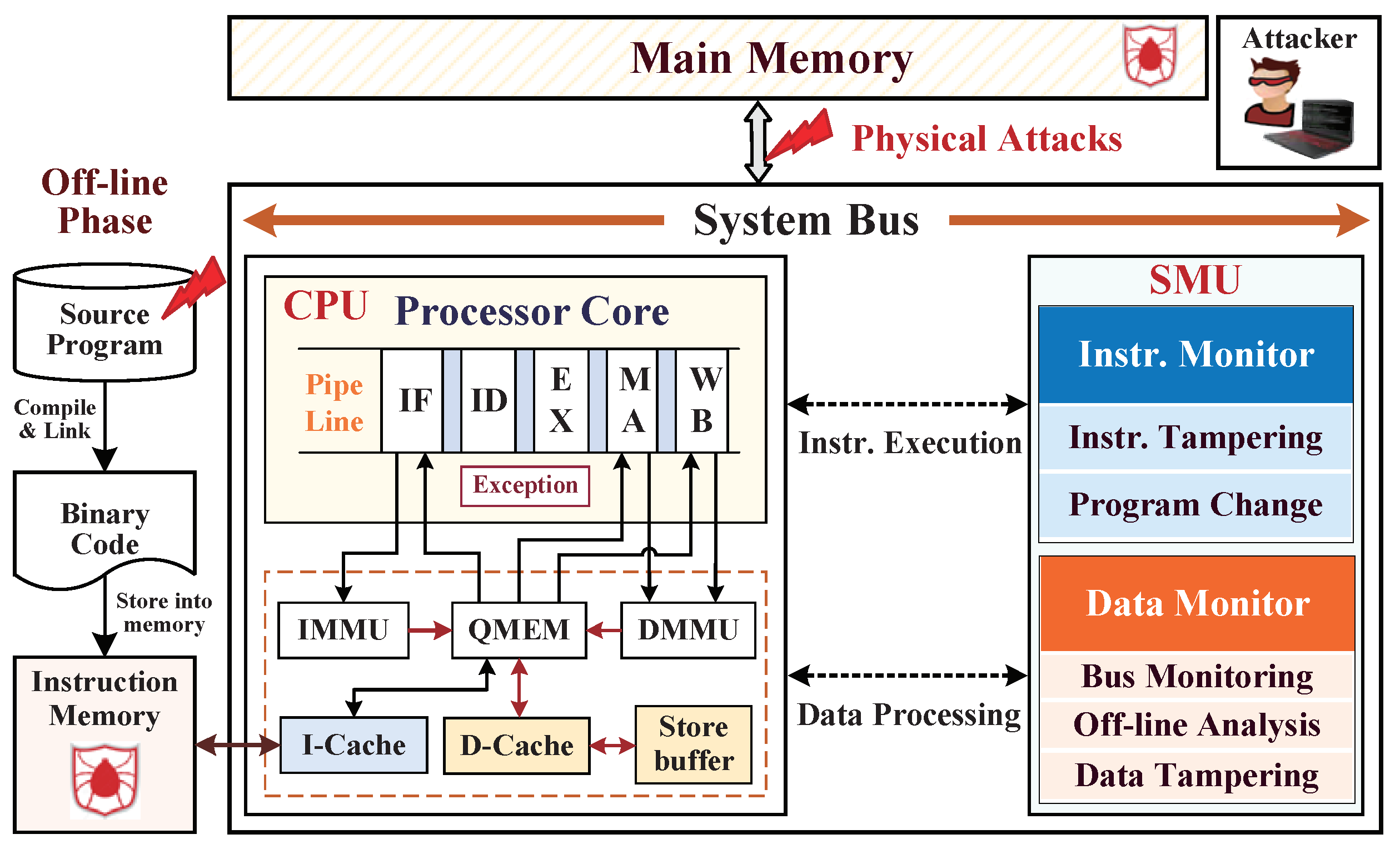
:1. Introduction
- An instruction monitor is constructed in SMU to real-time monitor instruction executions, and any instruction tampering is detected by program basic block (BB) integrity checking mechanism;
- A data monitor is also constructed in SMU to complete the authenticated encryption and dynamic data monitoring for preventing dynamic data leakages and data tampering attacks, and any unauthorized change of ciphertext or signature in external main memory is detected by Tag integrity checking;
- The I-Cache, D-Cache, and monitor cache (M-Cache) are felicitously configured to significantly reduce the system performance overhead induced by SMU, and its average performance overhead reduces to as low as 2.18%;
- The experimental evaluations of security capability and hardware consumption confirm that the monitoring mechanism of SMU satisfies a good balance between high-security capability and low hardware complexity.
2. Security Assumptions and Threat Models
- The first situation is that the instructions that were tampered with artificially arise from the program code phase (including software and application) before compiling and linking. For example, the program codes are modified via malicious code injections in C and C++ programmings [19] to cause stack-based and heap-based buffer overflows.
- The second situation is that the program instructions were maliciously modified in external instruction memory (such as flash memory) induced by hardware Trojans. The designers were leaning memory-oriented hardware Trojan insertions to modify or leak memory critical data [20,21]; here, the instruction modifications in memory are manifested as the data bit flips.
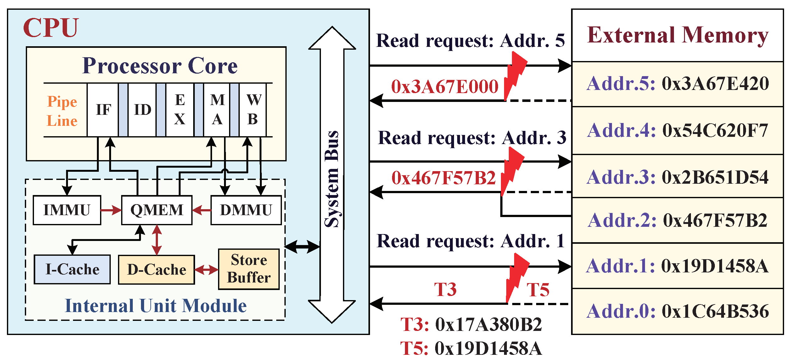
- The third situation is that the dynamic data were modified in external main memory by physical tampering attacks (or errors caused by a hardware Trojan). For example, external attacks aim at the vulnerable interface between SoC and external main memory, and their dynamic data exchange suffers from the three physical attacks of bus monitoring, offline analysis, and data tampering [22].
3. Preliminaries
3.1. Security Strategy of Instruction Execution Monitoring
3.1.1. Program Code Integrity
3.1.2. Control-Flow Integrity
3.1.3. Integrity Label Calculation
3.2. Security Strategy against Sensitive Data Leakage
3.2.1. Confidentiality Protection Scheme
3.2.2. Integrity Protection Scheme
3.2.3. Authentication of Digital Signature
3.3. External Tampering Attacks Aiming at Main Memory
4. Instruction Monitor against Instruction Tampering Attacks
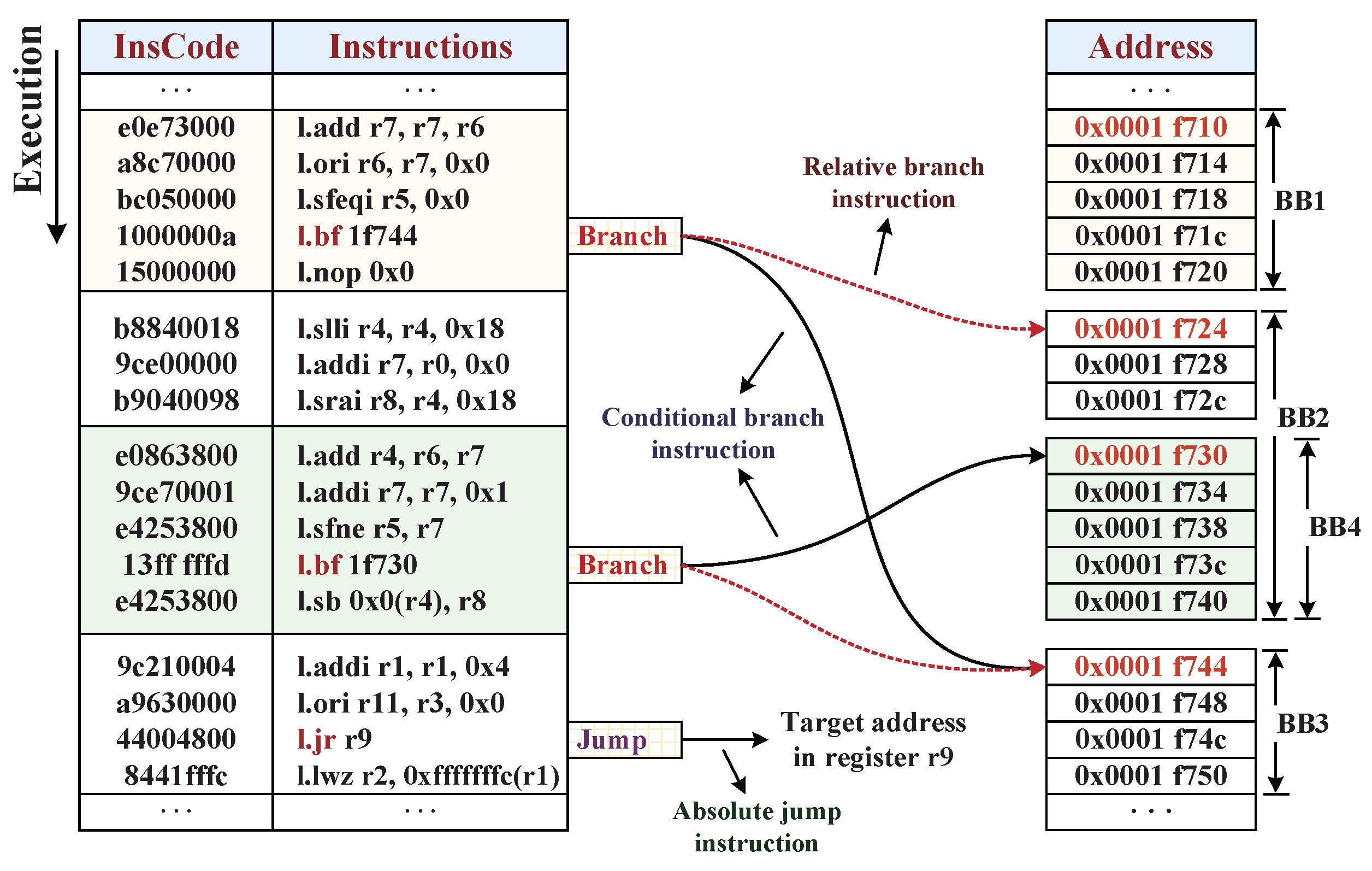
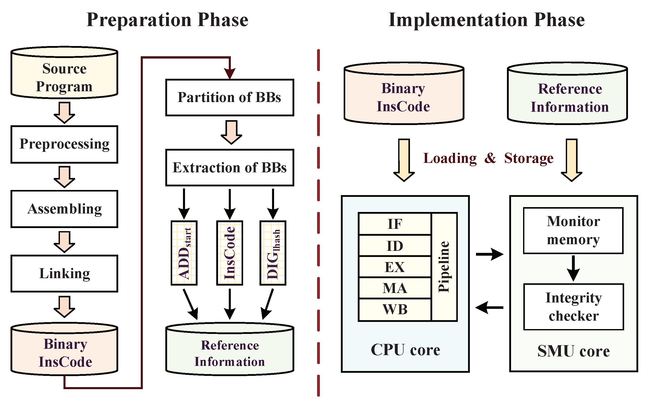
4.1. The Efficient Partition of Basic Blocks
4.2. Reference Information Extraction for Integrity Checking
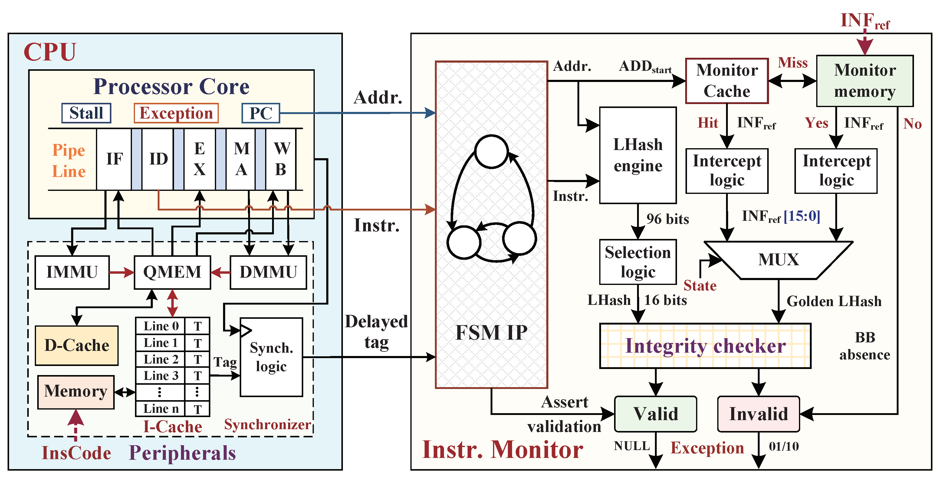
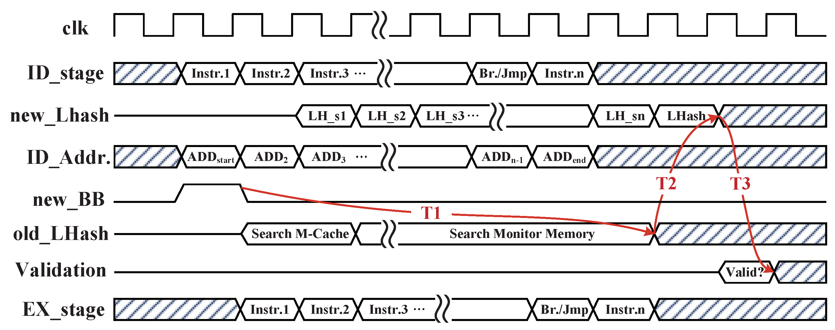
4.3. Hardware Implementation of Instruction Monitor
4.4. Performance Optimizations of Monitoring Mechanism
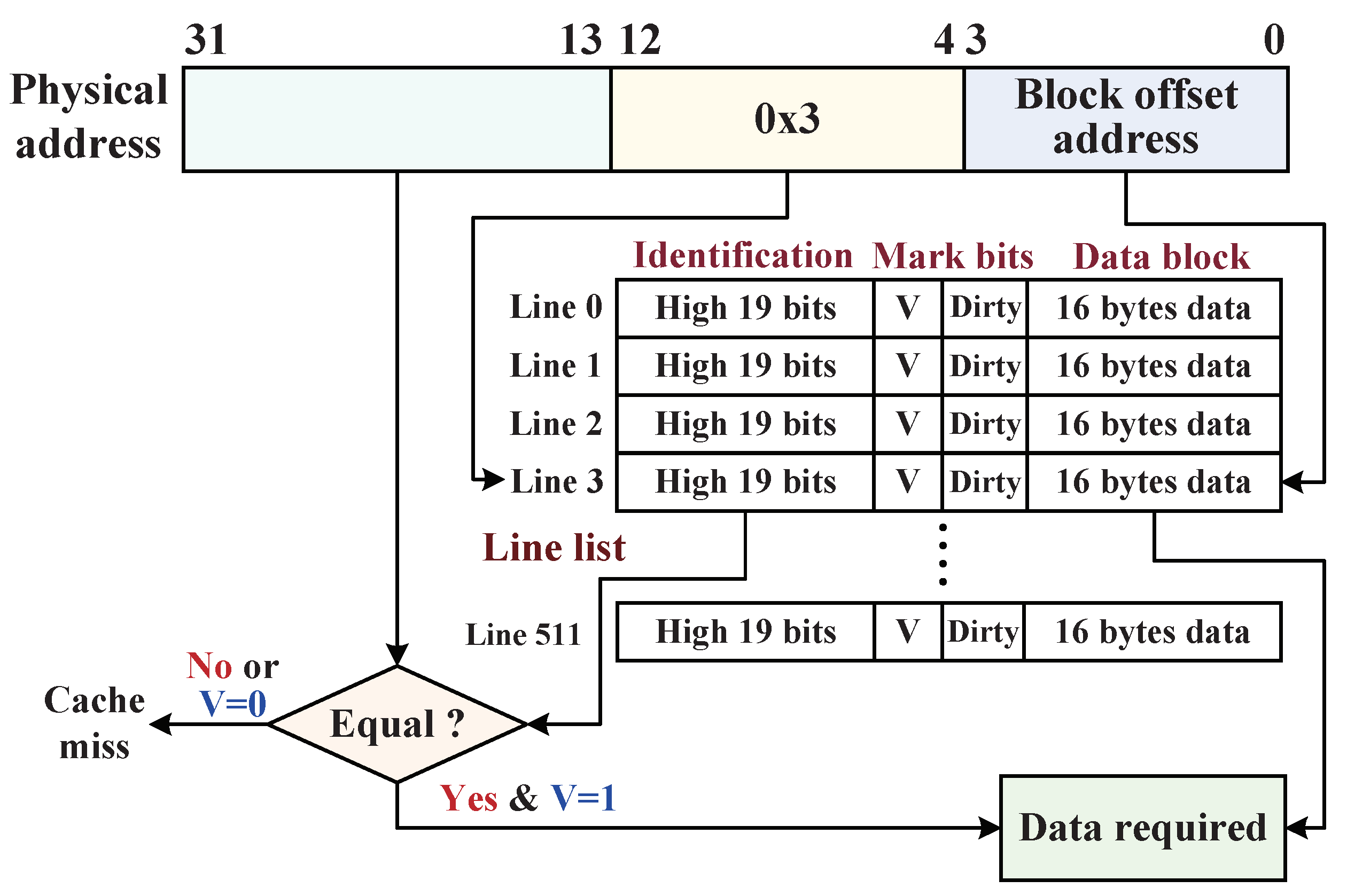
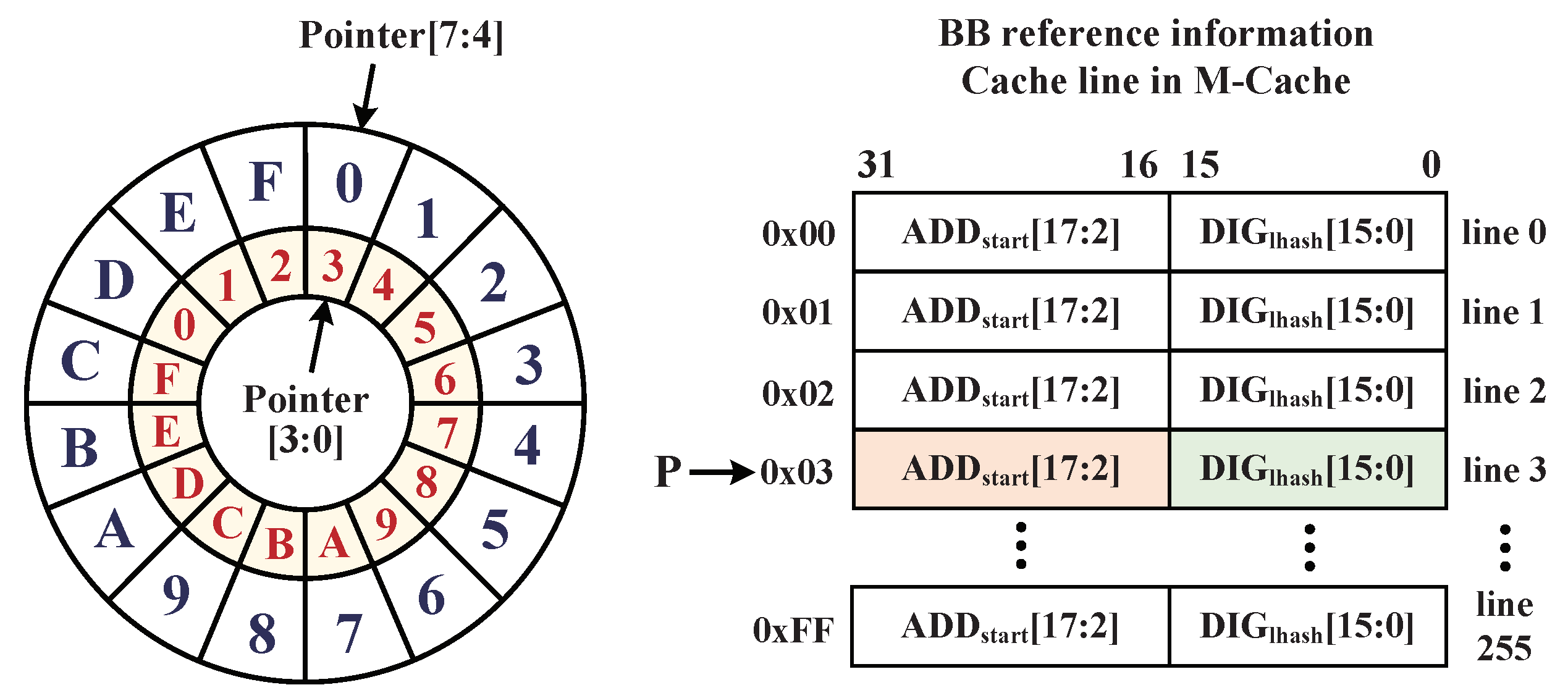
4.4.1. M-Cache Searching Method
4.4.2. I-Cache Optimized Approach
5. Data Monitor against External Physical Attacks
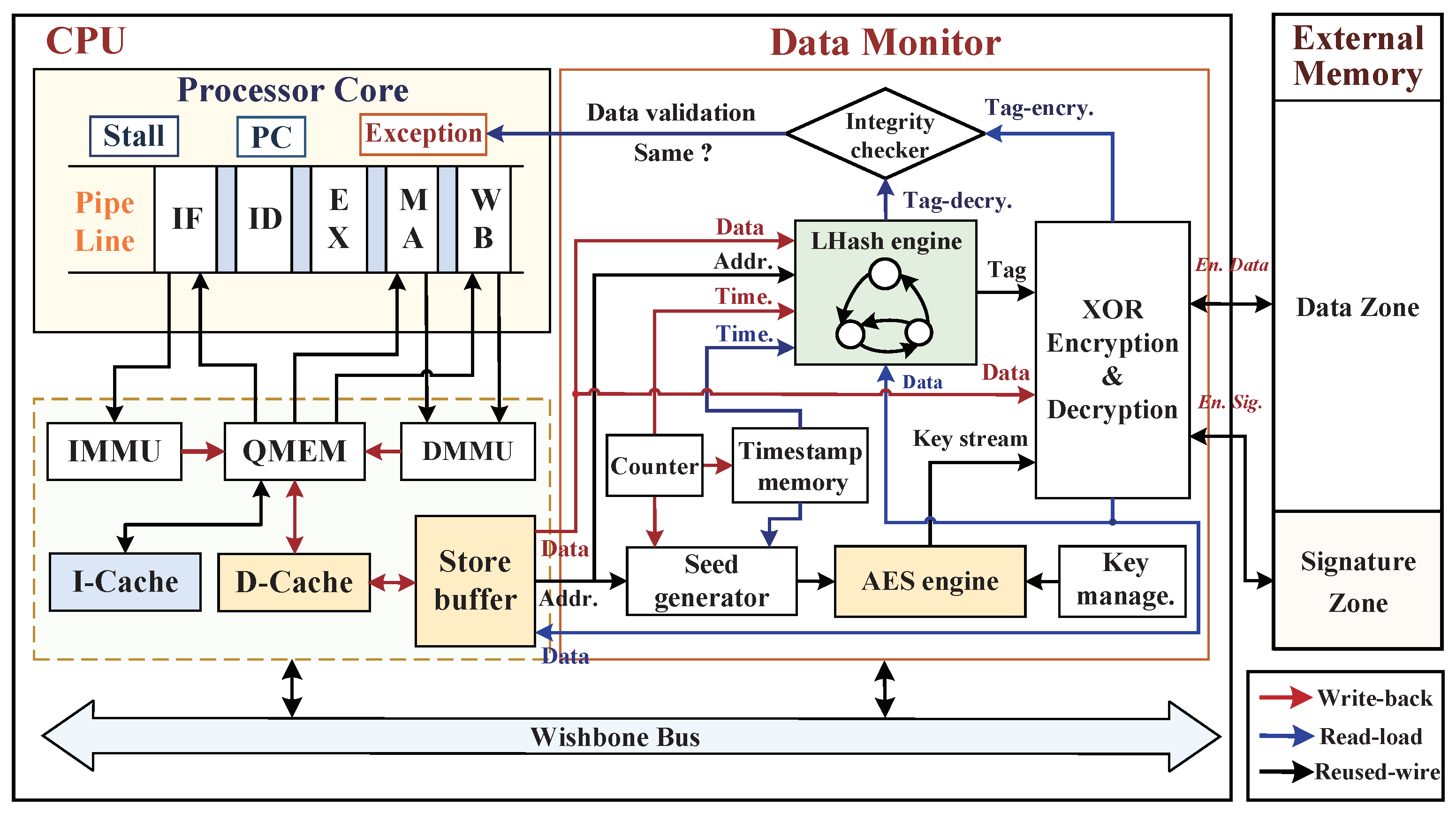
5.1. Hardware Architecture Implementation of Data Monitor
5.2. Data Write-Back Procedure of Memory Access
5.2.1. AES Ciphertext Generation
5.2.2. LHash Digital Signature Generation
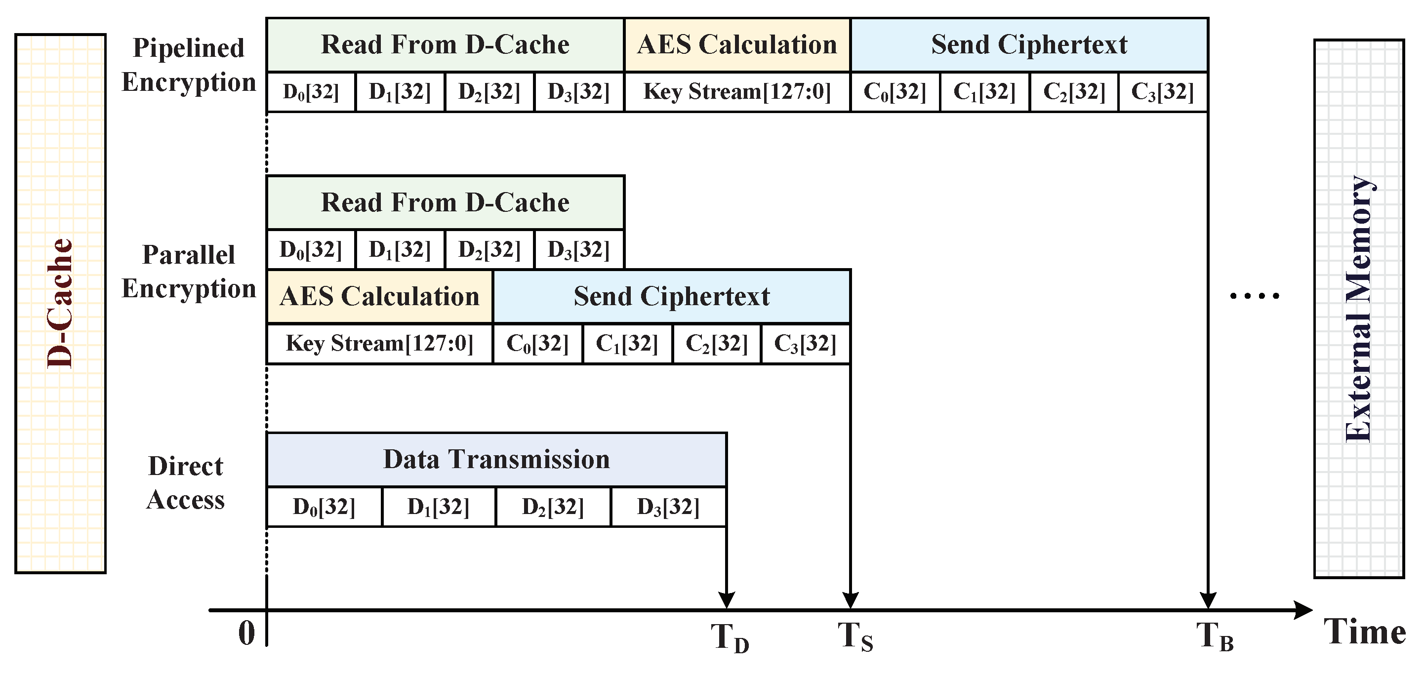
5.2.3. Data Write-Back Procedure with D-Cache
| Algorithm 1 Write-back operation of 128-bit data block stored into external main memory |
| Inputs:Data, Address |
| Outputs:Timestamps, Ciphertext, Signature |
|
5.3. Data Read-Load Procedure from External Memory
| Algorithm 2 Data-load operation of 128-bit ciphertext block from external main memory |
| Inputs:Address, Ciphertext, Signature |
| Outputs:Data, Exception |
|
6. Experiments and Results
6.1. Experimental Setup
6.2. Performance Overhead Evaluation
6.2.1. SMU Performance Overhead
6.2.2. Different Depths of M-Cache
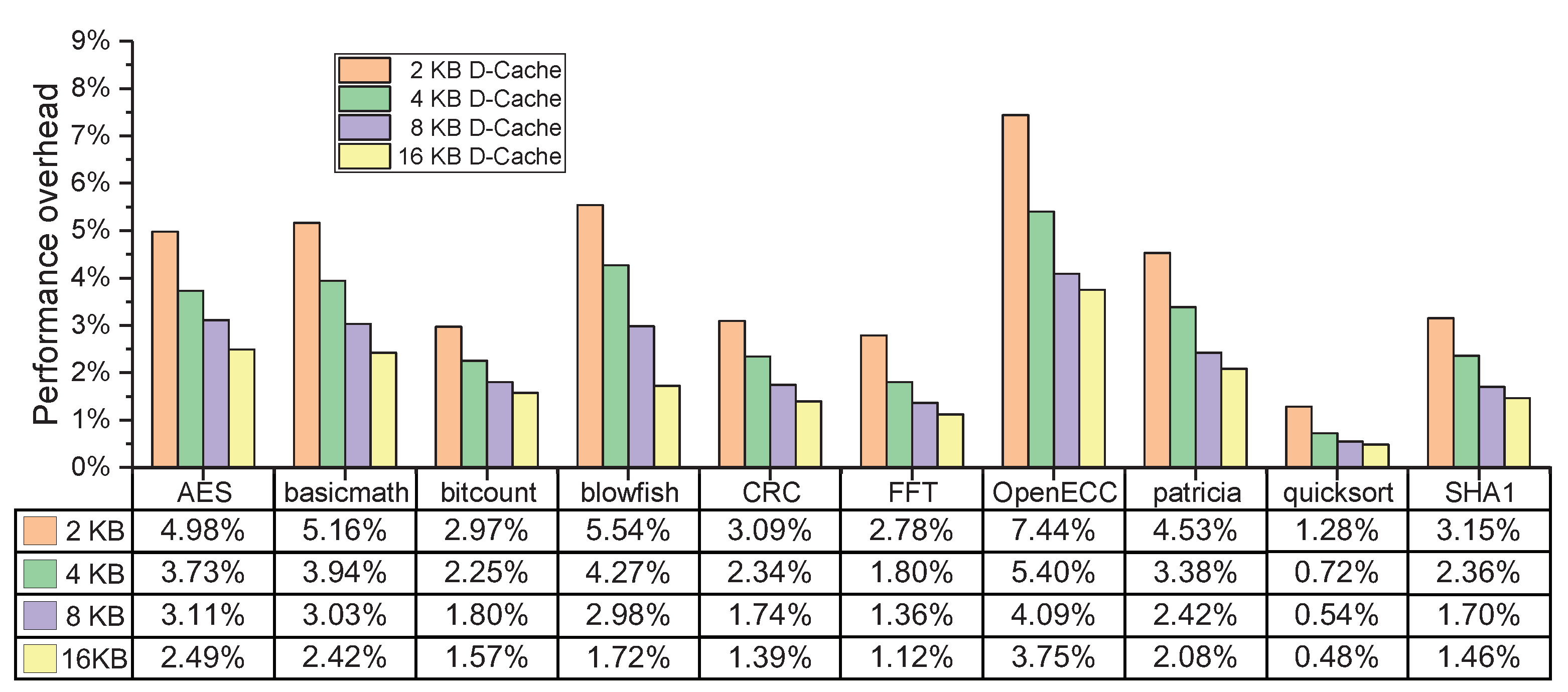
6.2.3. Different Sizes of D-Cache
6.3. Security Capability Evaluation
6.4. Comparison of Security and Practicality
- Level-I: Only defend against instruction tampering or data tampering.
- Level-II: Both defend against data tampering and data leakage.
- Level-III: Both defend against instruction tampering and data leakage.
- Level-IV: Both defend against instruction tampering, data tampering, and data leakage.
7. Hardware Implementation Evaluation
8. Conclusions
Author Contributions
Funding
Conflicts of Interest
References
- Lentaris, G.; Stratakos, I.; Stamoulias, I.; Soudris, D.; Lourakis, M.; Zabulis, X. High-performance vision-based navigation on SoC FPGA for spacecraft proximity operations. IEEE Trans. Circuits Syst. Video Technol. 2020, 30, 1188–1202. [Google Scholar] [CrossRef]
- Fayneh, E.; Yuffe, M.; Knoll, E.; Zelikson, M.; Abozaed, M.; Talker, Y.; Shmuely, Z.; Rahme, S.A. 14 nm 6th-generation core processor SoC with low power consumption and improved performance. In Proceedings of the IEEE International Solid-State Circuits Conference (ISSCC), San Francisco, CA, USA, 31 January–4 February 2016; pp. 72–73. [Google Scholar]
- Peña-Fernandez, M.; Lindoso, A.; Entrena, L.; Garcia-Valderas, M.; Morilla, Y.; Martín-Holgado, P. Online error detection through trace infrastructure in ARM microprocessors. IEEE Trans. Nucl. Sci. 2019, 66, 1457–1464. [Google Scholar] [CrossRef]
- Ray, S.; Peeters, E.; Tehranipoor, M.M.; Bhunia, S. System-on-chip platform security assurance: Architecture and validation. Proc. IEEE 2018, 106, 21–37. [Google Scholar] [CrossRef]
- Basak, A.; Bhunia, S.; Tkacik, T.; Ray, S. Security assurance for system-on-chip designs with untrusted IPs. IEEE Trans. Inf. Forensics Secur. 2017, 12, 1515–1528. [Google Scholar] [CrossRef]
- Das, S.; Liu, Y.; Zhang, W.; Chandramohan, M. Semantics-based online malware detection: Towards efficient real–time protection against malware. IEEE Trans. Inf. Forensics Secur. 2016, 11, 289–302. [Google Scholar] [CrossRef]
- Chen, Y.; Sun, W.; Zhang, N.; Zheng, Q.; Lou, W.; Hou, Y.T. Towards efficient fine-grained access control and trustworthy data processing for remote monitoring services in IoT. IEEE Trans. Inf. Forensics Secur. 2019, 14, 1830–1842. [Google Scholar] [CrossRef]
- De, A.; Khan, M.N.I.; Nagarajan, K.; Ghosh, S. HarTBleed: Using hardware Trojans for data leakage exploits. IEEE Trans. Very Large Scale Integr. Syst. 2020, 28, 968–979. [Google Scholar] [CrossRef]
- Khan, M.N.I.; De, A.; Ghosh, S. Cache-Out: Leaking cache memory using hardware Trojan. IEEE Trans. Very Large Scale Integr. Syst. 2020, 28, 1461–1470. [Google Scholar] [CrossRef]
- Chen, G.; Jin, H.; Zou, D.; Zhou, B.B.; Liang, Z.; Zheng, W.; Shi, X. Safestack: Automatically patching stack-based buffer overflow vulnerabilities. IEEE Trans. Dependable Secur. Comput. 2013, 10, 368–379. [Google Scholar] [CrossRef]
- Alam, M.; Roy, D.B.; Bhattacharya, S.; Govindan, V.; Chakraborty, R.S.; Mukhopadhyay, D. SmashClean: A hardware level mitigation to stack smashing attacks in OpenRISC. In Proceedings of the ACM/IEEE International Conference on Formal Methods and Models for System Design (MEMOCODE), Kanpur, India, 18–20 November 2016; pp. 1–4. [Google Scholar]
- Zhang, F.; Kodituwakku, H.A.D.E.; Hines, J.W.; Coble, J. Multilayer data-driven cyber-attack detection system for industrial control systems based on network, system, and process data. IEEE Trans. Ind. Inform. 2019, 15, 4362–4369. [Google Scholar] [CrossRef]
- Bhunia, S.; Hsiao, M.S.; Banga, M.; Narasimhan, S. Hardware Trojan attacks: Threat analysis and countermeasures. Proc. IEEE 2014, 102, 1229–1247. [Google Scholar] [CrossRef]
- Banga, M.; Hsiao, M.S. A novel sustained vector technique for the detection of hardware Trojans. In Proceedings of the 22nd International Conference on VLSI Design, New Delhi, India, 5–9 January 2009; pp. 327–332. [Google Scholar]
- Narasimhan, S.; Du, D.; Chakraborty, R.S.; Paul, S.; Wolff1, F.; Papachristou, C.; Roy, K.; Bhunia, S. Multiple-parameter side-channel analysis: A non-invasive hardware Trojan detection approach. In Proceedings of the IEEE International Symposium on Hardware-Oriented Security and Trust (HOST), Anaheim, CA, USA, 13–14 June 2010; pp. 13–18. [Google Scholar]
- Koushanfar, F.; Mirhoseini, A. A unified framework for multimodal submodular integrated circuits Trojan detection. IEEE Trans. Inf. Forensics Secur. 2011, 6, 162–174. [Google Scholar] [CrossRef] [Green Version]
- Ghandali, S.; Moos, T.; Moradi, A.; Paar, C. Side-channel hardware trojan for provably-secure SCA-protected implementations. IEEE Trans. Very Large Scale Integr. Syst. 2020, 28, 1435–1448. [Google Scholar] [CrossRef] [Green Version]
- Wang, W.; Zhang, X.; Hao, Q.; Zhang, Z.; Xu, B.; Dong, H.; Xia, T.; Wang, X. Hardware-enhanced protection for the runtime data security in embedded systems. Electronics 2019, 8, 52. [Google Scholar] [CrossRef] [Green Version]
- Younan, Y.; Joosen, W.; Piessens, F. Code Injection in C and CPP: A Survey of Vulnerabilities and Countermeasures; Katholieke Universiteit Leuven: Leuven, Belgium, 2004. [Google Scholar]
- Hoque, T.; Wang, X.; Basak, A.; Karam, R.; Bhunia, S. Hardware Trojan attacks in embedded memory. In Proceedings of the IEEE 36th VLSI Test Symposium (VTS), San Francisco, CA, USA, 22–25 April 2018; pp. 1–6. [Google Scholar]
- Nagarajan, K.; De, A.; Khan, M.; Ghosh, S. Trapped: DRAM Trojan designs for information leakage and fault injection attacks. arXiv 2020, arXiv:2001.00856. [Google Scholar]
- Hong, M.; Guo, H. FEDTIC: A security design for embedded systems with insecure external memory. In Proceedings of the International Conference on Future Generation Information Technology, Jeju Island, Korea, 13–15 December 2010; Springer: Berlin/Heidelberg, Germany, 2010; pp. 365–375. [Google Scholar]
- Wang, X.; Zhao, Z.; Xu, D.; Zhang, Z.; Hao, Q.; Liu, M. An M-Cache-based security monitoring and fault recovery architecture for embedded processor. IEEE Trans. Very Large Scale Integr. Syst. 2020, 28, 2314–2327. [Google Scholar] [CrossRef]
- Bresch, C.; Michelet, A.; Amato, L.; Meyer, T.; Hely, D. A red team blue team approach towards a secure processor design with hardware shadow stack. In Proceedings of the IEEE 2nd International Verification and Security Workshop (IVSW), Thessaloniki, Greece, 3–5 July 2017; pp. 57–62. [Google Scholar]
- Hu, H.; Shinde, S.; Adrian, S.; Chua, Z.L.; Saxena, P.; Liang, Z. Data-oriented programming: On the expressiveness of non-control data attacks. In Proceedings of the IEEE Symposium on Security and Privacy (SP), San Jose, CA, USA, 22–26 May 2016; pp. 969–986. [Google Scholar]
- Wu, W.; Wu, S.; Zhang, L.; Zou, J.; Dong, L. Lhash: A lightweight hash function. In Proceedings of the International Conference on Information Security and Cryptology; Springer: Cham, Switzerland, 2013; pp. 291–308. [Google Scholar]
- Gupta, S.S.; Chattopadhyay, A.; Sinha, K.; Maitra, S.; Sinha, B.P. High-performance hardware implementation for RC4 stream cipher. IEEE Trans. Comput. 2013, 62, 730–743. [Google Scholar] [CrossRef]
- Wang, G. An abuse-free fair contract-signing protocol based on the RSA signature. IEEE Trans. Inf. Forensics Secur. 2010, 5, 158–168. [Google Scholar] [CrossRef]
- Kermani, M.M.; Masoleh, A.R. Efficient and high-performance parallel hardware architectures for the AES-GCM. IEEE Trans. Comput. 2012, 61, 1165–1178. [Google Scholar] [CrossRef]
- Wang, X.; Zhao, Z.; Xu, D.; Zhang, Z.; Hao, Q.; Liu, M.; Si, Y. Two-stage checkpoint based security monitoring and fault recovery architecture for embedded processor. Electronics 2020, 9, 1165. [Google Scholar] [CrossRef]
- Guthaus, M.R.; Ringenberg, J.S.; Ernst, D.; Austin, T.M.; Mudge, T.; Brown, R.B. MiBench: A free, commercially representative embedded benchmark suite. In Proceedings of the 4th Annual IEEE International Workshop Workload Characterization, WWC-4, Austin, TX, USA, 2 December 2001; pp. 3–14. [Google Scholar]
- Bakiri, M.; Titri, S.; Izeboudjen, N.; Abid, F.; Louiz, F.; Lazib, D. Embedded system with Linux Kernel based on OpenRISC 1200-V3. In Proceedings of the International Conference on Sciences of Electronics, Sousse, Tunisia, 21–24 March 2012; pp. 177–182. [Google Scholar]
- Arora, D.; Ravi, S.; Raghunathan, A.; Jha, N.K. Hardware-assisted run-time monitoring for secure program execution on embedded processors. IEEE Trans. Very Large Scale Integr. Syst. 2006, 14, 1295–1308. [Google Scholar] [CrossRef]
- Tychalas, D.; Keliris, A.; Maniatakos, M. Stealthy information leakage through peripheral exploitation in modern embedded systems. IEEE Trans. Device Mater. Reliab. 2020, 20, 308–318. [Google Scholar] [CrossRef]
- Song, C.; Lee, B.; Lu, K.; Harris, W.R.; Kim, T.; Lee, W. Enforcing kernel security invariants with data flow integrity. In Proceedings of the 23th Annual Network and Distributed System Security Symposium, San Diego, CA, USA, 21–24 February 2016; pp. 1–15. [Google Scholar]
- Shi, W.; Fryman, J.B.; Gu, G.; Lee, H.S.; Zhang, Y.; Yang, J. InfoShield: A security architecture for protecting information usage in memory. In Proceedings of the Twelfth International Symposium on High-Performance Computer Architecture, Austin, TX, USA, 11–15 February 2006; pp. 222–231. [Google Scholar]
- Qiu, P.; Lyu, Y.; Zhang, J.; Wang, D.; Qu, G. Control flow integrity based on lightweight encryption architecture. IEEE Trans. Comput.-Aided Des. Integr. Circuits Syst. 2018, 37, 1358–1369. [Google Scholar] [CrossRef]
- Mashtizadeh, A.J.; Bittau, A.; Boneh, D.; Mazières, D. CCFI: Cryptographically enforced control flow integrity. In Proceedings of the 22nd ACM SIGSAC Conference on Computer and Communications Security, Denver, CO, USA, 12–16 October 2015; pp. 941–951. [Google Scholar]
- Guo, J.; Peyrin, T.; Poschmann, A. The PHOTON family of lightweight hash functions. Adv. Cryptol. 2011, 6841, 222–239. [Google Scholar]


| Benchmark | Total Instr. | Total BB | Memory Size (KB) | I-Cache Hit | D-Cache Read Hit | D-Cache Write Hit | CPI without SMU | CPI with SMU | Perform. Overhead |
|---|---|---|---|---|---|---|---|---|---|
| AES | 22,170 | 3535 | 13.81 | 99.23% | 99.86% | 99.73% | 3.53 | 3.64 | 3.11% |
| basicmath | 26,515 | 4327 | 16.90 | 98.18% | 98.65% | 98.62% | 2.64 | 2.72 | 3.03% |
| bitcount | 19,684 | 3344 | 13.06 | 97.98% | 96.52% | 96.48% | 1.67 | 1.70 | 1.80% |
| blowfish | 19,128 | 3247 | 12.68 | 97.75% | 97.74% | 97.67% | 3.54 | 3.61 | 1.98% |
| CRC | 18,941 | 3231 | 12.62 | 99.61% | 98.41% | 98.35% | 1.72 | 1.75 | 1.74% |
| FFT | 13,506 | 2143 | 8.37 | 96.29% | 98.52% | 98.41% | 2.94 | 2.98 | 1.36% |
| OpenECC | 56,313 | 6734 | 26.30 | 99.15% | 99.17% | 98.96% | 3.18 | 3.31 | 4.09% |
| patricia | 23,130 | 3853 | 15.05 | 97.68% | 97.26% | 97.05% | 1.65 | 1.69 | 2.42% |
| quicksort | 6707 | 1018 | 3.98 | 99.23% | 99.10% | 98.83% | 1.86 | 1.87 | 0.54% |
| SHA1 | 20,455 | 3400 | 13.28 | 98.75% | 99.38% | 99.27% | 2.35 | 2.39 | 1.70% |
| Average | – | – | 13.61 | 98.39% | 98.46% | 98.34% | 2.51 | 2.57 | 2.18% |
| Benchmark | CPI without SMU | CPI with SMU under the Different Depths of M-Cache | |||||
|---|---|---|---|---|---|---|---|
| No M-Cache | Depth (16) | Depth (32) | Depth (64) | Depth (128) | Depth (256) | ||
| AES | 3.53 | 5.16 | 4.52 | 3.98 | 3.78 | 3.65 | 3.64 |
| basicmath | 2.64 | 3.94 | 3.29 | 2.95 | 2.81 | 2.73 | 2.72 |
| bitcount | 1.67 | 2.37 | 2.15 | 1.87 | 1.79 | 1.71 | 1.70 |
| blowfish | 3.54 | 5.03 | 4.46 | 3.94 | 3.81 | 3.62 | 3.61 |
| CRC | 1.72 | 2.27 | 2.15 | 2.01 | 1.83 | 1.76 | 1.75 |
| FFT | 2.94 | 5.12 | 4.30 | 3.67 | 3.37 | 2.99 | 2.98 |
| OpenECC | 3.18 | 4.78 | 4.07 | 3.59 | 3.44 | 3.32 | 3.31 |
| patricia | 1.65 | 2.35 | 2.10 | 1.83 | 1.76 | 1.70 | 1.69 |
| quicksort | 1.86 | 2.64 | 2.38 | 2.08 | 1.89 | 1.87 | 1.87 |
| SHA1 | 2.35 | 3.69 | 2.95 | 2.64 | 2.50 | 2.40 | 2.39 |
| Average | 2.51 | 3.74 | 3.24 | 2.86 | 2.60 | 2.58 | 2.57 |
| Performance overhead | – | 48.92% | 29.07% | 13.88% | 3.59% | 2.67% | 2.18% |
| Tampering Attacks | Nontransfer Instr. Tampering | Transfer Instr. Tampering | Spoofing Attack | Relocation Attack | Replay Attack |
|---|---|---|---|---|---|
| Approaches | l.nop 0x0 l.nop 0x1 | l.bf 1f730 l.bf 1f734 | Write: 0x0000201E Read: 0x0000201E | Write: 0x00002016 Read: 0x00002012 | T5: 32’h19d1458a T3: 32’h17a380b2 |
| Instruction Tampering | 15000000 15000001 | 13ff fffd 14000001 | – | – | – |
| Data Tampering | – | – | 32’h3a67e420 32’h3a67e000 | 32’h2b651d54 32’h467f57b2 | 32’h19d1458a 32’h17a380b2 |
| Exception | LHash Error (“01”) | LHash Error (“01”) BB Absence (“10”) | Integrity Error (“11”) | Integrity Error (“11”) | Integrity Error (“11”) |
| Security Mechanism | Security Capability | Comprehensive Practicality | |||||
|---|---|---|---|---|---|---|---|
| Level | Instruction Tampering | Data Tampering | Data Leakage | ISA Extension | Compiler Modification | Performance Overhead | |
| HAM [33] | I | Yes | No | No | No | No | Medi (5.59%) |
| SM-FR [23] | I | Yes | No | No | No | No | High (9.33%) |
| HardRoot [34] | I | No | Yes | No | No | No | Low (2.80%) |
| KENALI [35] | I | No | Yes | No | No | No | High (7–15%) |
| FEDTIC [22] | II | No | Yes | Yes | No | No | Medi (7.60%) |
| InfoShield [36] | II | No | Yes | Yes | Yes | Yes | Low (<1.0%) |
| HEP [18] | II | No | Yes | Yes | No | No | Low (0.94%) |
| CFI-LEA [37] | III | Yes | No | Yes | Yes | Yes | Low (3.19%) |
| WLUD-NBL [9] | III | Yes | No | Yes | No | No | Low (3.60%) |
| CCFI [38] | III | Yes | No | Yes | Yes | Yes | High (52.0%) |
| Our SMU | IV | Yes | Yes | Yes | No | No | Low (2.18%) |
| Type | Resource Utilization | SoC | SMU |
|---|---|---|---|
| FPGA | Slice Registers | 2674 | 1058 |
| Slice LUTs | 17,836 | 2235 | |
| Occupied Slices | 7762 | 837 | |
| BlockRAM/FIFO | 58 | 53 | |
| ASIC | Chip Area | 2.94 mm | 1.07 mm |
| Power Consumption | 57.2 mW | 7.9 mW |
Publisher’s Note: MDPI stays neutral with regard to jurisdictional claims in published maps and institutional affiliations. |
© 2021 by the authors. Licensee MDPI, Basel, Switzerland. This article is an open access article distributed under the terms and conditions of the Creative Commons Attribution (CC BY) license (https://creativecommons.org/licenses/by/4.0/).
Share and Cite
Wang, X.; Zhang, Z.; Hao, Q.; Xu, D.; Wang, J.; Jia, H.; Zhou, Z. Hardware-Assisted Security Monitoring Unit for Real-Time Ensuring Secure Instruction Execution and Data Processing in Embedded Systems. Micromachines 2021, 12, 1450. https://doi.org/10.3390/mi12121450
Wang X, Zhang Z, Hao Q, Xu D, Wang J, Jia H, Zhou Z. Hardware-Assisted Security Monitoring Unit for Real-Time Ensuring Secure Instruction Execution and Data Processing in Embedded Systems. Micromachines. 2021; 12(12):1450. https://doi.org/10.3390/mi12121450
Chicago/Turabian StyleWang, Xiang, Zhun Zhang, Qiang Hao, Dongdong Xu, Jiqing Wang, Haoyu Jia, and Zhiyu Zhou. 2021. "Hardware-Assisted Security Monitoring Unit for Real-Time Ensuring Secure Instruction Execution and Data Processing in Embedded Systems" Micromachines 12, no. 12: 1450. https://doi.org/10.3390/mi12121450
APA StyleWang, X., Zhang, Z., Hao, Q., Xu, D., Wang, J., Jia, H., & Zhou, Z. (2021). Hardware-Assisted Security Monitoring Unit for Real-Time Ensuring Secure Instruction Execution and Data Processing in Embedded Systems. Micromachines, 12(12), 1450. https://doi.org/10.3390/mi12121450