
Naphthalocyanine-Based NIR Organic Photodiode: Understanding the Role of Different Types of Fullerenes

 ,
,  ,
, 
Abstract
:1. Introduction
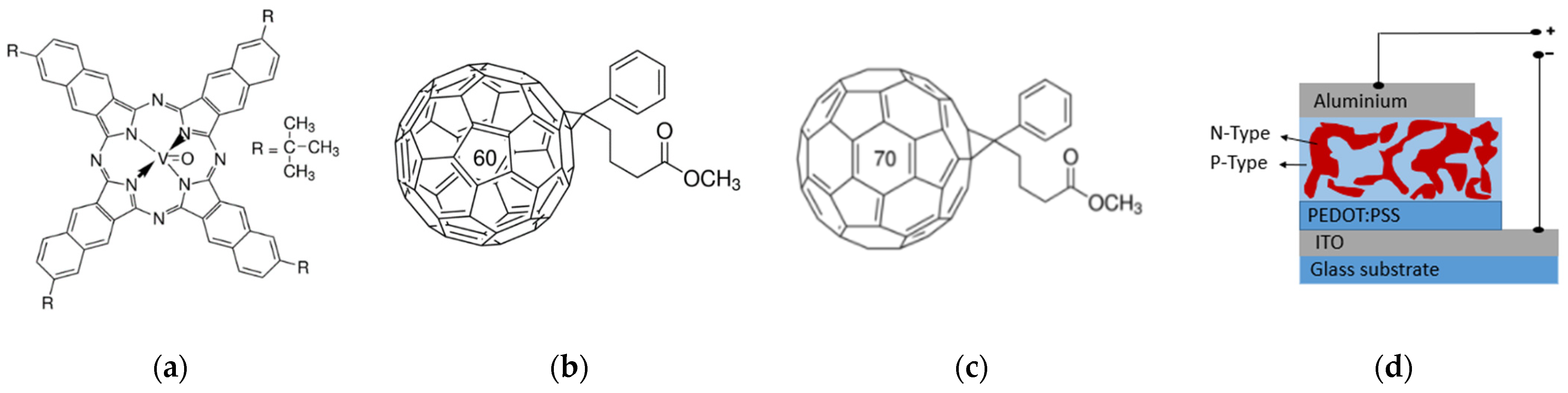
2. Experimental
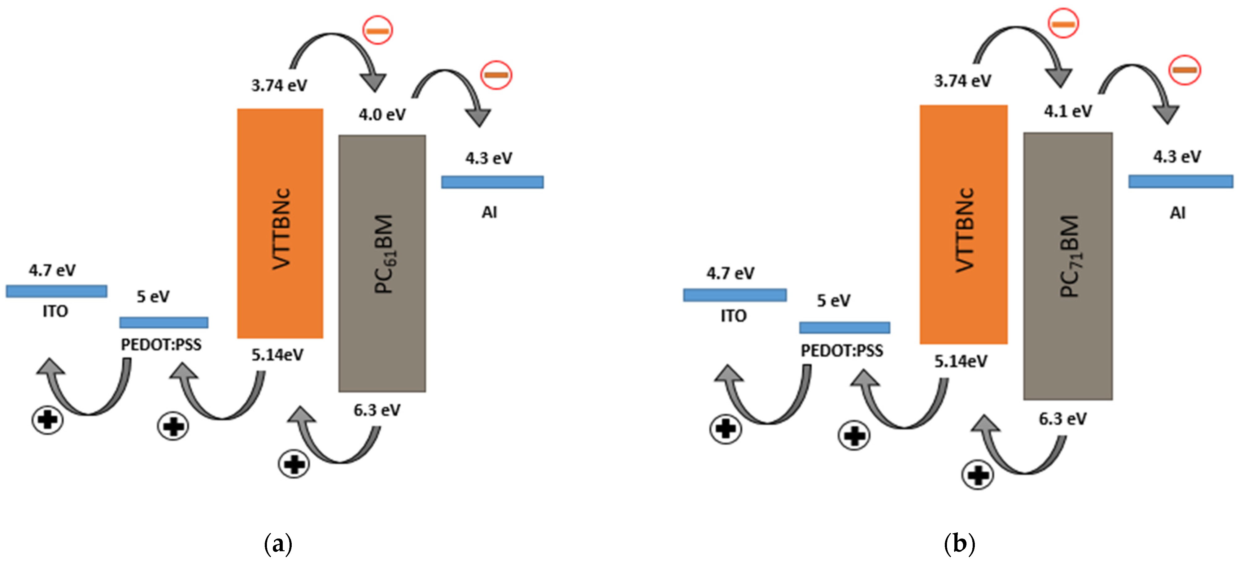
3. Results and Discussion
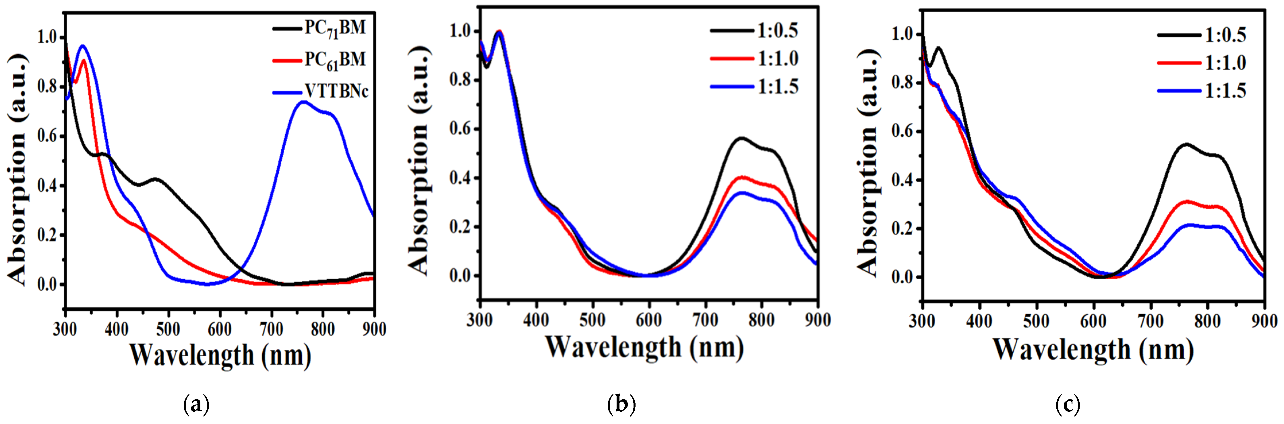
3.1. Absorption Characteristics
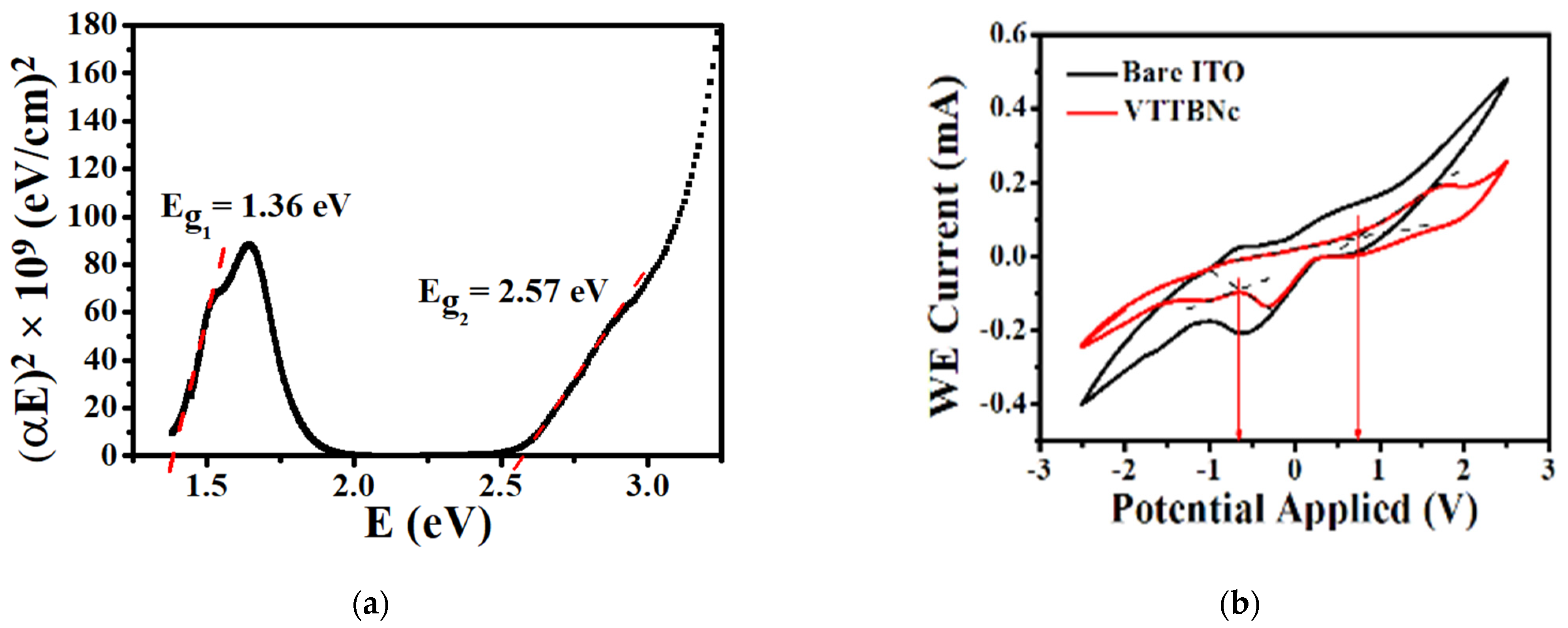
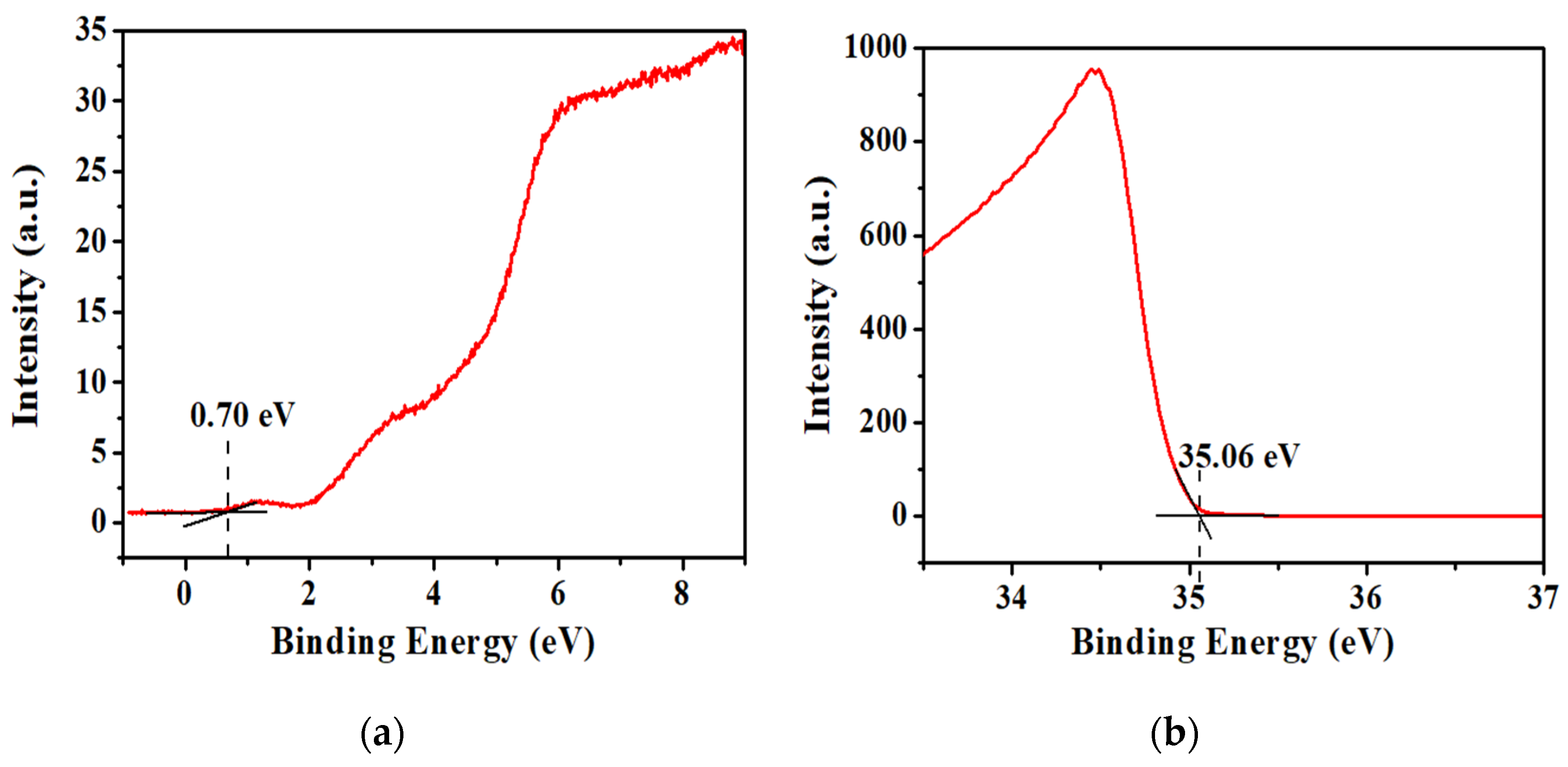
3.2. Determination of VTTBNc Energy Bandgap
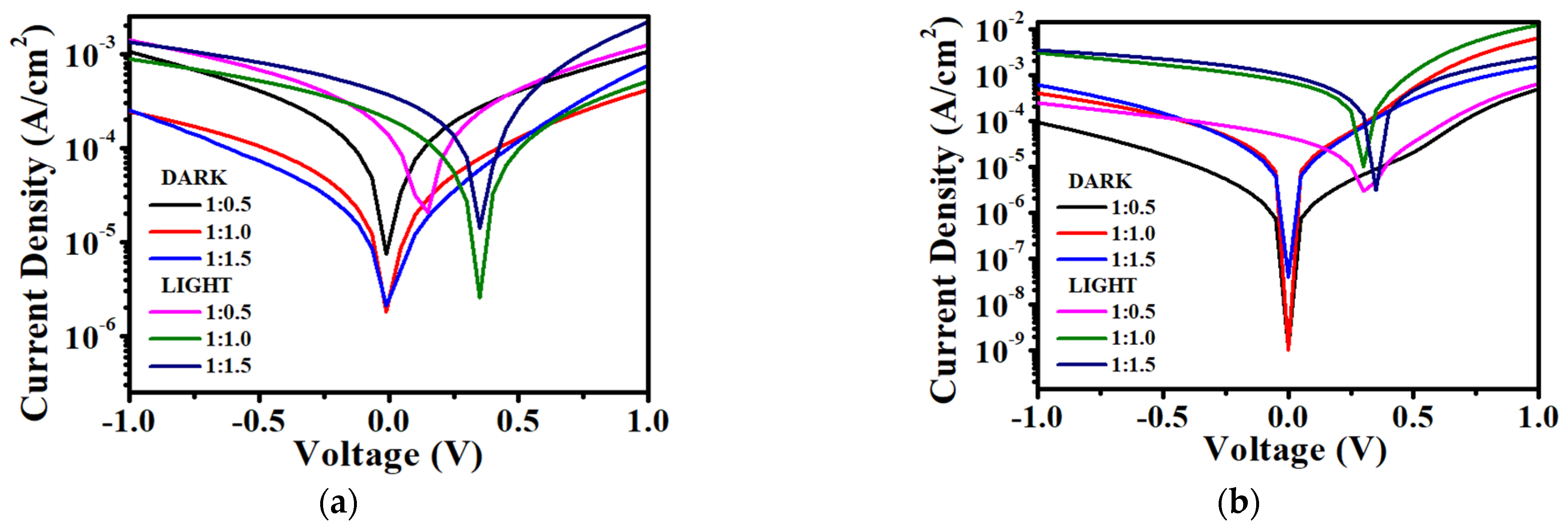
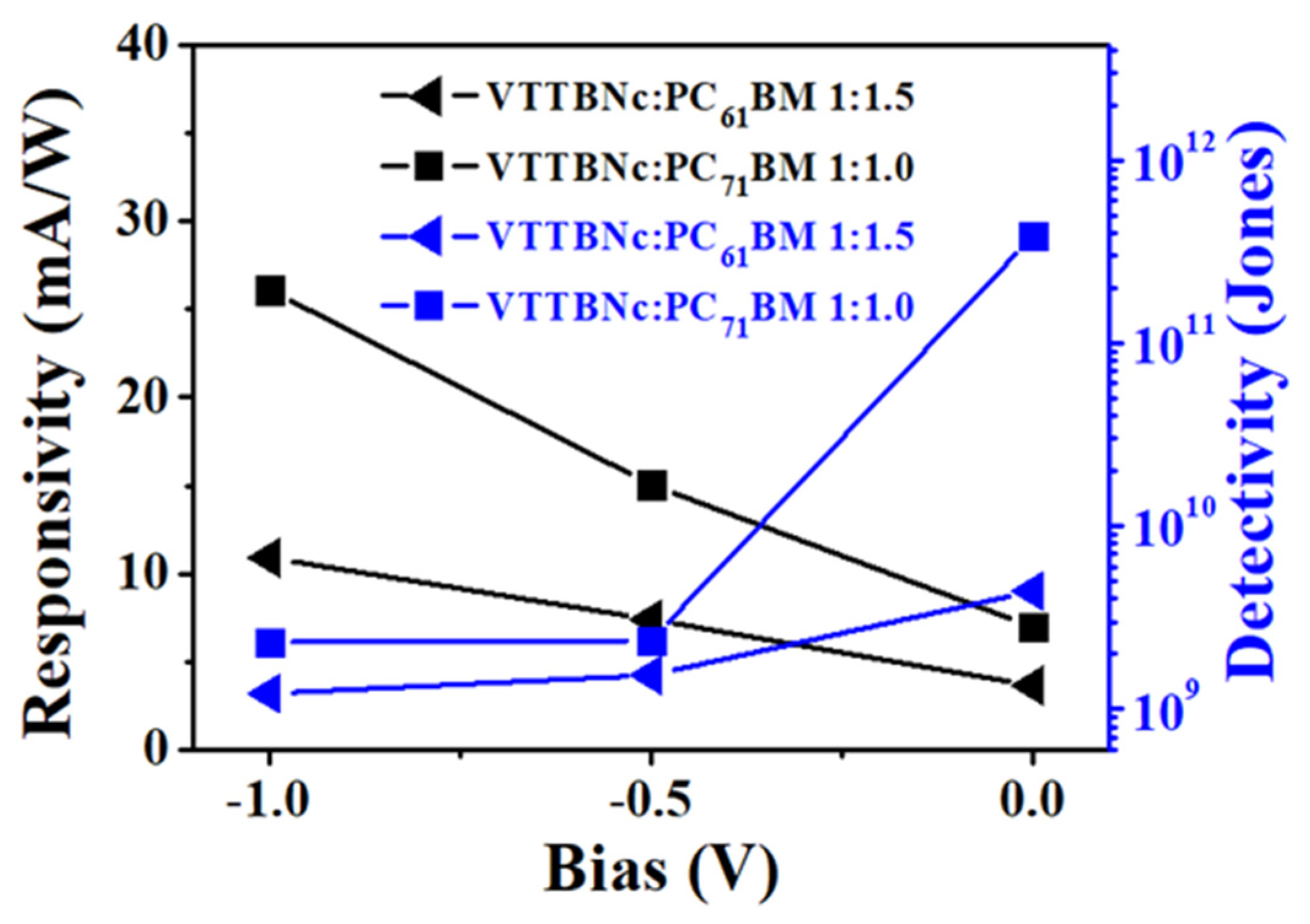
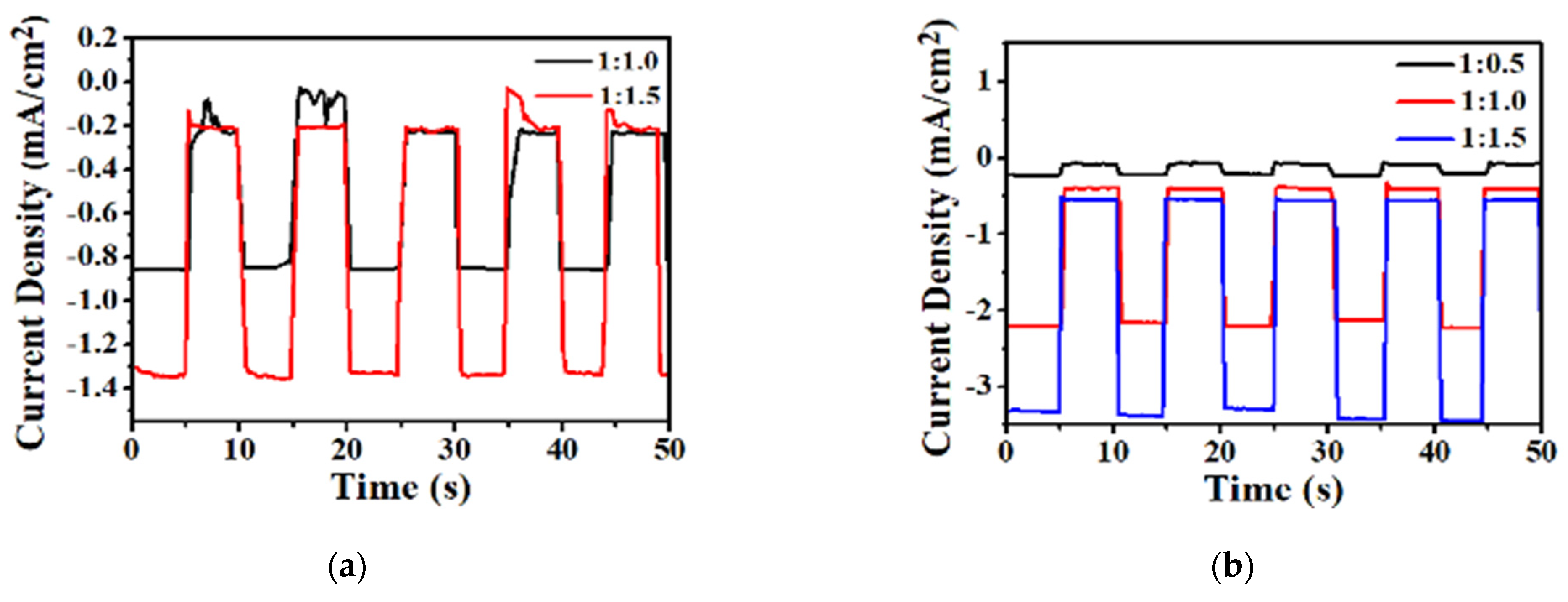
3.3. Performance of VTTBNc:PC61BM and VTTBNc:PC71BM Organic Photodiode
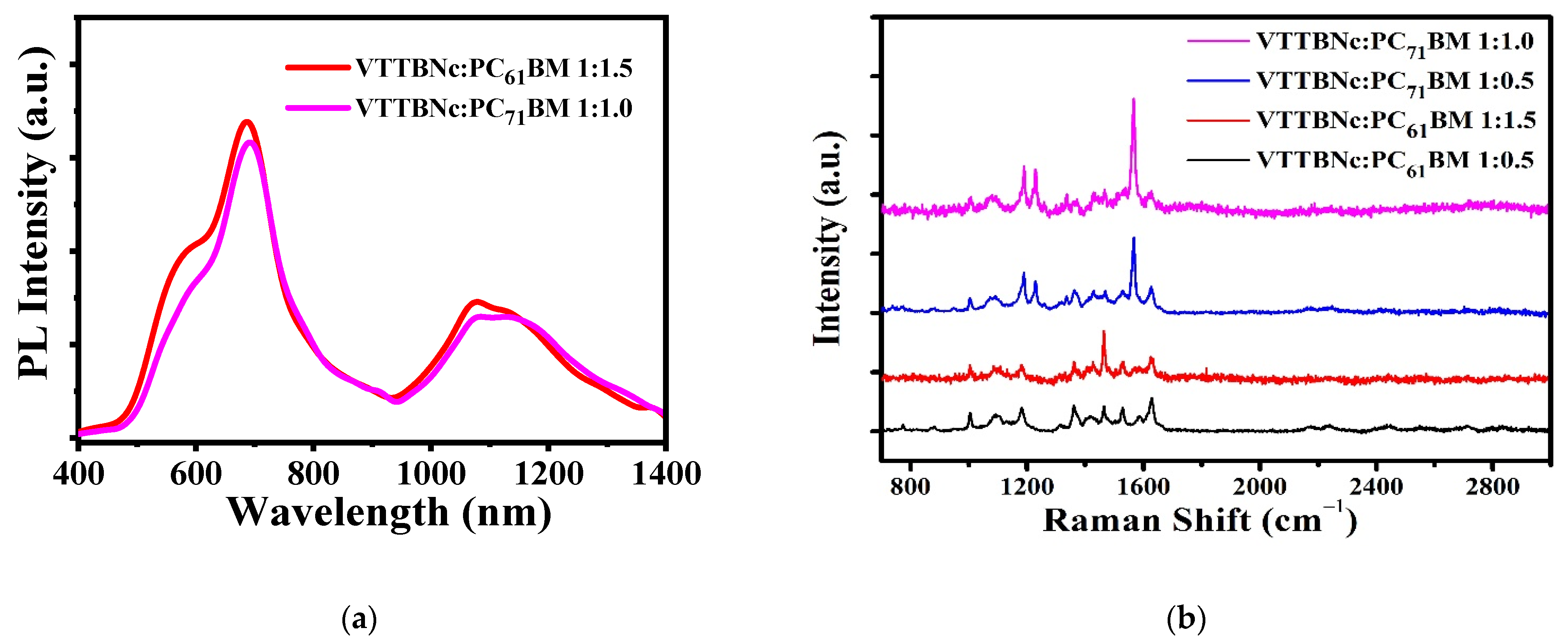
3.4. Photoluminescence and Raman Spectra
3.5. Morphological and Surface Roughness Observations
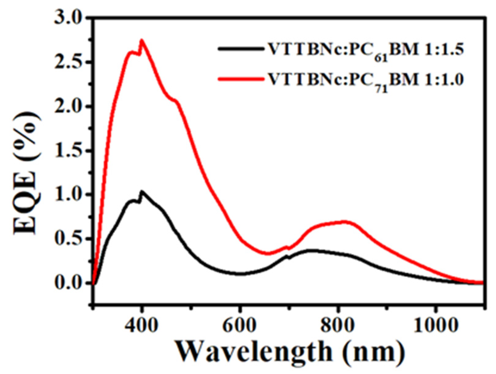
3.6. External Quantum Efficiency (EQE)
4. Conclusions
Author Contributions
Funding
Conflicts of Interest
References
- Hong, S.; Kang, H.; Kim, G.; Lee, S.; Kim, S.; Lee, J.H.; Lee, J.; Yi, M.; Kim, J.; Back, H.; et al. A series connection architecture for large-area organic photovoltaic modules with a 7.5% module efficiency. Nat. Commun. 2016, 7, 1–6. [Google Scholar] [CrossRef]
- Lin, Y.; Li, Y.; Zhan, X. Small molecule semiconductors for high-efficiency organic photovoltaics. Chem. Soc. Rev. 2012, 41, 4245–4272. [Google Scholar] [CrossRef]
- Liu, G.; Chen, M.; Wang, J.; Xi, X.; Dong, W.; Chen, G.; Chen, L.; Chen, R. Investigation and application of the optical field distribution in gradient organic heterojunction. Opt. Commun. 2018, 429, 60–64. [Google Scholar] [CrossRef]
- Tong, S.; Yuan, J.; Zhang, C.; Wang, C.; Liu, B.; Shen, J.; Xia, H.; Zou, Y.; Xie, H.; Sun, J.; et al. Large-scale roll-to-roll printed, flexible and stable organic bulk heterojunction photodetector. NPJ Flex. Electron. 2018, 2, 1–8. [Google Scholar] [CrossRef] [Green Version]
- Zhao, Z.; Wang, J.; Miao, J.; Zhang, F. Photomultiplication type organic photodetectors with tunable spectral response range. Org. Electron. 2019, 69, 354–360. [Google Scholar] [CrossRef]
- Roslan, N.A.; Abdullah, S.M.; Abd Majid, W.H.; Supangat, A. Investigation of VTP: PC71BM organic composite as highly responsive organic photodetector. Sens. Actuators A Phys. 2018, 279, 361–366. [Google Scholar] [CrossRef]
- Simone, G.; Dyson, M.J.; Weijtens, C.H.; Meskers, S.C.; Coehoorn, R.; Janssen, R.A.; Gelinck, G.H. On the origin of dark current in organic photodiodes. Adv. Opt. Mater. 2020, 8, 1901568. [Google Scholar] [CrossRef] [Green Version]
- Zafar, Q.; Fatima, N.; Karimov, K.S.; Ahmed, M.M.; Sulaiman, K. Realizing broad-bandwidth visible wavelength photodiode based on solution-processed ZnPc/PC71BM dyad. Opt. Mater. 2017, 64, 131–136. [Google Scholar] [CrossRef]
- Zhang, G.; Zhang, K.; Yin, Q.; Jiang, X.F.; Wang, Z.; Xin, J.; Ma, W.; Yan, H.; Huang, F.; Cao, Y. High-performance ternary organic solar cell enabled by a thick active layer containing a liquid crystalline small molecule donor. J. Am. Chem. Soc. 2017, 139, 2387–2395. [Google Scholar] [CrossRef] [PubMed]
- Natali, D.; Caironi, M. Organic photodetectors. In Photodetectors; Elsevier: Amsterdam, The Netherlands, 2016; pp. 195–254. [Google Scholar]
- Wienk, M.M.; Kroon, J.M.; Verhees, W.J.; Knol, J.; Hummelen, J.C.; Van Hal, P.A.; Janssen, R.A. Efficient methano [70] fullerene/MDMO-PPV bulk heterojunction photovoltaic cells. Angew. Chem. Int. Ed. 2003, 42, 3371–3375. [Google Scholar] [CrossRef] [PubMed]
- Vakhshouri, K.; Kozub, D.R.; Wang, C.; Salleo, A.; Gomez, E.D. Effect of miscibility and percolation on electron transport in amorphous poly (3-hexylthiophene)/phenyl-C61-butyric acid methyl ester blends. Phys. Rev. Lett. 2012, 108, 026601. [Google Scholar] [CrossRef] [Green Version]
- Campbell, I. Transparent organic photodiodes with high quantum efficiency in the near infrared. Appl. Phys. Lett. 2010, 97, 149. [Google Scholar] [CrossRef]
- Matthew, M.S.; Pandey, R.; Holmes, R.J. Tandem organic photodetectors with tunable, broadband response. Appl. Phys. Lett. 2012, 101, 223301. [Google Scholar] [CrossRef]
- Blumenfeld, M.L.; Steele, M.P.; Ilyas, N.; Monti, O.L. Interfacial electronic structure of vanadyl naphthalocyanine on highly ordered pyrolytic graphite. Surf. Sci. 2010, 604, 1649–1657. [Google Scholar] [CrossRef]
- Jiang, J.; Liu, W.; Arnold, D.P. Sandwich complexes of naphthalocyanine with the rare earth metals. J. Porphyr. Phthalocyanines 2003, 7, 459–473. [Google Scholar] [CrossRef]
- Cheng, P.; Yang, Y. Narrowing the band gap: The key to high-performance organic photovoltaics. Acc. Chem. Res. 2020, 53, 1218–1228. [Google Scholar] [CrossRef] [PubMed]
- Dong, H.; Zhu, H.; Meng, Q.; Gong, X.; Hu, W. Organic photoresponse materials and devices. Chem. Soc. Rev. 2012, 41, 1754–1808. [Google Scholar] [CrossRef]
- Collins, S.D.; Ran, N.A.; Heiber, M.C.; Nguyen, T.Q. Small is powerful: Recent progress in solution-processed small molecule solar cells. Adv. Energy Mater. 2017, 7, 1602242. [Google Scholar] [CrossRef]
- Dhanya, I.; Menon, C. Surface morphological, structural, electrical and optical properties of annealed vanadyl tetra tert-butyl 2, 3 naphthalocyanine thin films. Vacuum 2012, 86, 1289–1295. [Google Scholar] [CrossRef]
- Namepetra, A.; Kitching, E.; Ala’a, F.E.; Hill, I.G.; Welch, G.C. Understanding the morphology of solution processed fullerene-free small molecule bulk heterojunction blends. Phys. Chem. Chem. Phys. 2016, 18, 12476–12485. [Google Scholar] [CrossRef] [Green Version]
- Arbogast, J.W.; Foote, C.S. Photophysical properties of C70. J. Am. Chem. Soc. 1991, 113, 8886–8889. [Google Scholar] [CrossRef]
- Benatto, L.; Marchiori, C.F.; Talka, T.; Aramini, M.; Yamamoto, N.A.D.; Huotari, S.; Roman, L.S.; Koehler, M. Comparing C60 and C70 as acceptor in organic solar cells: Influence of the electronic structure and aggregation size on the photovoltaic characteristics. Thin Solid Film. 2020, 697, 137827. [Google Scholar] [CrossRef]
- Tauc, J.; Grigorovici, R.; Vancu, A. Optical properties and electronic structure of amorphous germanium. Phys. Status Solidi 1966, 15, 627–637. [Google Scholar] [CrossRef]
- Pandey, R.; Kerner, R.A.; Menke, S.M.; Holst, J.; Josyula, K.V.; Holmes, R.J. Tin naphthalocyanine complexes for infrared absorption in organic photovoltaic cells. Org. Electron. 2013, 14, 804–808. [Google Scholar] [CrossRef]
- Kissinger, P.T.; Heineman, W.R. Cyclic voltammetry. J. Chem. Educ. 1983, 60, 702. [Google Scholar] [CrossRef]
- Nolasco, J.C.; Ryan, J.W.; Rodríguez, M.; Castro-Carranza, A.; Maldonado, J.L.; Ramos-Ortiz, G.; Barbosa-Garcia, O.; Gutowski, J.; Palomares, E.; Parisi, J. Organoboron donor-π-acceptor chromophores for small-molecule organic solar cells. J. Mater. Sci. Mater. Electron. 2018, 29, 16410–16415. [Google Scholar] [CrossRef]
- Peljo, P.; Girault, H.H. Electrochemical potential window of battery electrolytes: The HOMO–LUMO misconception. Energy Environ. Sci. 2018, 11, 2306–2309. [Google Scholar] [CrossRef]
- Trasatti, S. The absolute electrode potential: An explanatory note. Pure Appl. Chem. 1986, 58, 955–966. [Google Scholar] [CrossRef]
- Elgrishi, N.; Rountree, K.J.; McCarthy, B.D.; Rountree, E.S.; Eisenhart, T.T.; Dempsey, J.L. A practical beginner’s guide to cyclic voltammetry. J. Chem. Educ. 2018, 95, 197–206. [Google Scholar] [CrossRef]
- Misra, A.; Kumar, P.; Srivastava, R.; Dhawan, S.K.; Kamalasanan, M.N.; Chandra, S. Electrochemical and Optical Studies of Conjugated Polymers for Three Primary Colours. Indian J. Pure Appl. Phys. 2005, 43, 921–925. [Google Scholar]
- Schulz, G.L.; Urdanpilleta, M.; Fitzner, R.; Brier, E.; Mena-Osteritz, E.; Reinold, E.; Bäuerle, P. Optimization of solution-processed oligothiophene: Fullerene based organic solar cells by using solvent additives. Beilstein J. Nanotechnol. 2013, 4, 680–689. [Google Scholar] [CrossRef]
- Simone, G.; Dyson, M.J.; Meskers, S.C.; Janssen, R.A.; Gelinck, G.H. Organic photodetectors and their application in large area and flexible image sensors: The role of dark current. Adv. Funct. Mater. 2020, 30, 1904205. [Google Scholar] [CrossRef] [Green Version]
- Wang, C.; Zhang, X.; Hu, W. Organic photodiodes and phototransistors toward infrared detection: Materials, devices, and applications. Chem. Soc. Rev. 2020, 49, 653–670. [Google Scholar] [CrossRef]
- Motaung, D.E.; Malgas, G.F.; Arendse, C.J.; Mavundla, S.E.; Knoesen, D. Structural and photo-physical properties of spin-coated poly (3-hexylthiophene) thin films. Mater. Chem. Phys. 2009, 116, 279–283. [Google Scholar] [CrossRef]
- Zhou, Y.; Tvingstedt, K.; Zhang, F.; Du, C.; Ni, W.X.; Andersson, M.R.; Inganäs, O. Observation of a charge transfer state in low-bandgap polymer/fullerene blend systems by photoluminescence and electroluminescence studies. Adv. Funct. Mater. 2009, 19, 3293–3299. [Google Scholar] [CrossRef]
- Makinudin, A.H.A.; Fakir, M.S.; Supangat, A. Metal phthalocyanine: Fullerene composite nanotubes via templating method for enhanced properties. Nanoscale Res. Lett. 2015, 10, 53. [Google Scholar]
- Kotula, A.P.; Snyder, C.R.; Migler, K.B. Determining conformational order and crystallinity in polycaprolactone via Raman spectroscopy. Polymer 2017, 117, 1–10. [Google Scholar] [CrossRef] [Green Version]
- Bartelt, J.A.; Lam, D.; Burke, T.M.; Sweetnam, S.M.; McGehee, M.D. Charge-Carrier Mobility Requirements for Bulk Heterojunction Solar Cells with High Fill Factor and External Quantum Efficiency > 90%. Adv. Energy Mater. 2015, 5, 1500577. [Google Scholar] [CrossRef]
- Proctor, C.M.; Love, J.A.; Nguyen, T.Q. Mobility Guidelines for High Fill Factor Solution-Processed Small Molecule Solar Cells. Adv. Mater. 2014, 26, 5957–5961. [Google Scholar] [CrossRef]
- Williams, M.; Tummala, N.R.; Aziz, S.G.; Risko, C.; Brédas, J.L. Influence of molecular shape on solid-state packing in disordered PC61BM and PC71BM fullerenes. J. Phys. Chem. Lett. 2014, 5, 3427–3433. [Google Scholar] [CrossRef]
- Kesava, S.V.; Fei, Z.; Rimshaw, A.D.; Wang, C.; Hexemer, A.; Asbury, J.B.; Heeney, M.; Gomez, E.D. Domain compositions and fullerene aggregation govern charge photogeneration in polymer/fullerene solar cells. Adv. Energy Mater. 2014, 4, 1400116. [Google Scholar] [CrossRef]
- Long, G.; Li, A.; Shi, R.; Zhou, Y.C.; Yang, X.; Zuo, Y.; Wu, W.R.; Jeng, U.S.; Wang, Y.; Wan, X.; et al. The Evidence for Fullerene Aggregation in High-Performance Small-Molecule Solar Cells by Molecular Dynamics Simulation. Adv. Electron. Mater. 2015, 1, 1500217. [Google Scholar] [CrossRef]


| Sample | Bias (V) | JD (A/cm2) | Jph (A/cm2) | R (mA/W) | D* (Jones) | VOC (V) |
|---|---|---|---|---|---|---|
| PC61BM | 0 | 1.04 × 10⁻⁷ | 1.05 × 10⁻³ | 10.50 | 5.75 × 10¹⁰ | 0.5 |
| −0.5 | 3.08 × 10⁻⁴ | 1.74 × 10⁻³ | 14.32 | 1.44 × 10⁹ | ||
| −1.0 | 7.89 × 10⁻⁴ | 2.41 × 10−03 | 16.21 | 1.02 × 10⁹ | ||
| PC71BM | 0 | 8.42 × 10⁻⁸ | 1.64 × 10⁻³ | 16.40 | 9.98 × 10¹⁰ | 0.5 |
| −0.5 | 8.14 × 10⁻⁴ | 2.88 × 10⁻³ | 20.66 | 1.28 × 10⁹ | ||
| −1.0 | 2.15 × 10⁻³ | 4.27 × 10⁻³ | 21.20 | 8.08 × 10⁸ |
| Sample | Ratio | Bias (V) | JD (A/cm2) | Jph (A/cm2) | R (mA/W) | D* (Jones) | VOC (V) |
|---|---|---|---|---|---|---|---|
| VTTBNc:PC61BM | 1:0.5 | 0 V | 7.48 × 10⁻⁶ | 1.35 × 10⁻⁴ | 1.28 | 8.24 × 10⁸ | 0.15 |
| −0.5 V | 4.13 × 10⁻⁴ | 6.75 × 10⁻⁴ | 2.62 | 2.28 × 10⁸ | |||
| −1.0 V | 1.06 × 10⁻³ | 1.40 × 10⁻³ | 3.40 | 1.84 × 10⁸ | |||
| 1:1.0 | 0 V | 1.82 × 10⁻⁶ | 2.03 × 10⁻⁴ | 2.01 | 2.64 × 10⁹ | 0.35 | |
| −0.5 V | 1.07 × 10⁻⁴ | 5.17 × 10⁻⁴ | 4.10 | 7.00 × 10⁸ | |||
| −1.0 V | 2.43 × 10⁻⁴ | 8.84 × 10⁻⁴ | 6.41 | 7.26 × 10⁸ | |||
| 1:1.5 | 0 V | 2.11 × 10⁻⁶ | 3.65 × 10⁻⁴ | 3.63 | 4.41 × 10⁹ | 0.35 | |
| −0.5 V | 7.27 × 10⁻⁵ | 8.11 × 10⁻⁴ | 7.38 | 1.53 × 10⁹ | |||
| −1.0 V | 2.51 × 10⁻⁴ | 1.34 × 10⁻³ | 10.89 | 1.21 × 10⁹ | |||
| VTTBNc:PC71BM | 1:0.5 | 0 V | 1.08 × 10⁻⁹ | 4.35 × 10⁻⁵ | 0.43 | 2.34 × 10¹⁰ | 0.3 |
| −0.5 V | 1.81 × 10⁻⁵ | 1.18 × 10⁻⁴ | 1.00 | 4.15 × 10⁸ | |||
| −1.0 V | 9.25 × 10⁻⁵ | 2.43 × 10⁻⁴ | 1.51 | 2.76 × 10⁸ | |||
| 1:1.0 | 0 V | 1.02 × 10⁻⁹ | 6.96 × 10⁻⁴ | 6.96 | 3.85 × 10¹¹ | 0.3 | |
| −0.5 V | 1.26 × 10⁻⁴ | 1.63 × 10⁻³ | 15.04 | 2.37 × 10⁹ | |||
| −1.0 V | 3.99 × 10⁻⁴ | 3.01 × 10⁻³ | 26.11 | 2.31 × 10⁹ | |||
| 1:1.5 | 0 V | 3.96 × 10⁻⁸ | 9.55 × 10⁻⁴ | 9.55 | 8.48 × 10¹⁰ | 0.35 | |
| −0.5 V | 1.46 × 10⁻⁴ | 2.20 × 10⁻³ | 20.54 | 3.00 × 10⁹ | |||
| −1.0 V | 6.02 × 10⁻⁴ | 3.45 × 10⁻³ | 28.48 | 2.05 × 10⁹ |
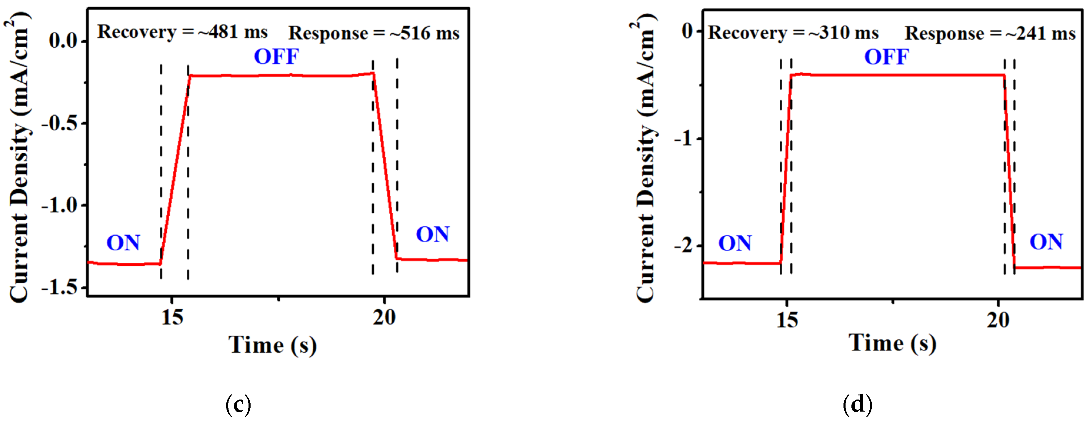
| Sample | Ratio | Recovery Time (ms) | Response Time (ms) |
|---|---|---|---|
| VTTBNc:PC61BM | 1:0.5 | - | - |
| 1:1.0 | 895 | 518 | |
| 1:1.5 | 481 | 516 | |
| VTTBNc:PC71BM | 1:0.5 | 311 | 242 |
| 1:1.0 | 310 | 241 | |
| 1:1.5 | 336 | 524 |
| Assignments | Raman Shift (cm−1) | |||
|---|---|---|---|---|
| VTTBNc:PC71BM | VTTBNc:PC61BM | |||
| 1:1.0 | 1:0.5 | 1:1.5 | 1:0.5 | |
| Benzene ring breath | 1003 | 1003 | 1003 | 1003 |
| Ring stretch | 1086 | 1086 | 1092 | 1092 |
| C–H bend | 1190, 1227 | 1190, 1227 | 1180 | 1180 |
| Pyrrole stretch | 1337 | 1337 | 1316 | 1316 |
| Ring stretch | 1363, 1430, 1467 | 1363, 1430, 1467 | 1363, 1420, 1467 | 1363, 1415, 1467 |
| Pyrrole stretch | 1534 | 1529 | 1530 | 1530 |
| C=C stretch | 1566, 1626 | 1566, 1629 | 1582, 1629 | 1587, 1629 |
| Scan Size | 5 μm × 5 μm | 0.5 μm× 0.5 μm |
|---|---|---|
| VTTBNc:PC61BM (1:0.5) | 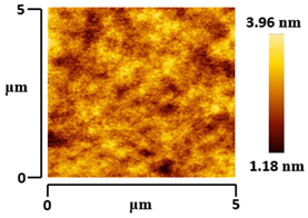 | 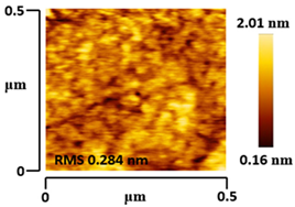 |
| VTTBNc:PC61BM (1:1.5) | 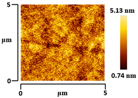 | 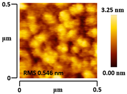 |
| VTTBNc:PC71BM (1:0.5) | 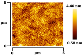 | 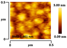 |
| VTTBNc:PC71BM (1:1.0) |  | 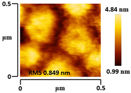 |
Publisher’s Note: MDPI stays neutral with regard to jurisdictional claims in published maps and institutional affiliations. |
© 2021 by the authors. Licensee MDPI, Basel, Switzerland. This article is an open access article distributed under the terms and conditions of the Creative Commons Attribution (CC BY) license (https://creativecommons.org/licenses/by/4.0/).
Share and Cite
Alwi, S.A.K.; Hisamuddin, S.N.; Abdullah, S.M.; Anuar, A.; Abdul Rahim, A.H.; Majid, S.R.; Bawazeer, T.M.; Alsoufi, M.S.; Alsenany, N.; Supangat, A. Naphthalocyanine-Based NIR Organic Photodiode: Understanding the Role of Different Types of Fullerenes. Micromachines 2021, 12, 1383. https://doi.org/10.3390/mi12111383
Alwi SAK, Hisamuddin SN, Abdullah SM, Anuar A, Abdul Rahim AH, Majid SR, Bawazeer TM, Alsoufi MS, Alsenany N, Supangat A. Naphthalocyanine-Based NIR Organic Photodiode: Understanding the Role of Different Types of Fullerenes. Micromachines. 2021; 12(11):1383. https://doi.org/10.3390/mi12111383
Chicago/Turabian StyleAlwi, Siti Anis Khairani, Syaza Nafisah Hisamuddin, Shahino Mah Abdullah, Afiq Anuar, Atiqah Husna Abdul Rahim, Siti Rohana Majid, Tahani M. Bawazeer, Mohammad S. Alsoufi, Nourah Alsenany, and Azzuliani Supangat. 2021. "Naphthalocyanine-Based NIR Organic Photodiode: Understanding the Role of Different Types of Fullerenes" Micromachines 12, no. 11: 1383. https://doi.org/10.3390/mi12111383
APA StyleAlwi, S. A. K., Hisamuddin, S. N., Abdullah, S. M., Anuar, A., Abdul Rahim, A. H., Majid, S. R., Bawazeer, T. M., Alsoufi, M. S., Alsenany, N., & Supangat, A. (2021). Naphthalocyanine-Based NIR Organic Photodiode: Understanding the Role of Different Types of Fullerenes. Micromachines, 12(11), 1383. https://doi.org/10.3390/mi12111383