2D Nanomaterial-Based Surface Plasmon Resonance Sensors for Biosensing Applications


 ,
,
Abstract
1. Introduction
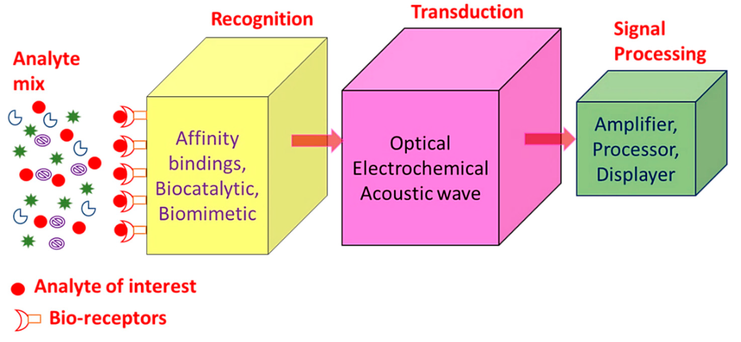
- Analyte: A material whose chemical constituents are described and measured. Glucose, for example, is an ‘analyte’ designed to detect glucose in a biosensor.
- Recognition: A recognition element also known as a bio-receptor, which is a biological element (DNA probe, enzyme, antibody, etc.) susceptible to analyte recognition (antigen, complementary DNA, enzyme substrate, etc). It is important for the bio-receptor to be directly sensitive to the target analyte in order to avoid interference from certain signal sources or substances from the sample matrix.
- Transducer: The transducer is a component which converts one energy source into other. Inside a biosensor, the function of the transducer is to turn the bio-recognition event into an observed signal. This cycle of energy transfer is known as signalling. Some transducers emit optical or electrical signals that are typically proportional to the amount of analyte-bio-receptor interactions.
- Signal processing: The work of the signal-processing unit is to process the transduced signal and prepare it for display. It consists of complex electronic circuitry conducting signal conditioning, such as analogue-to-digital amplification and signal transfer. The interpreted signals are then quantified via the display device with the biosensor. The display has a user interpretation system, such as a liquid crystal display on a computer or a direct printer, which generate numbers or curves that the user can understand. Often this part has a combination of hardware and software which generates user-friendly biosensor results. Depending on the end user’s requirements, the output signal on the monitor may be numerical, graphical, tabular or picture [1,2,3,4,5].
2. Fundamentals of SPR Sensing
3. Theoretical and Mathematical Modelling
3.1. Theoretical Modelling
3.2. Mathematical Modeling
4. Characteristic Parameters
5. Role of Material Selection
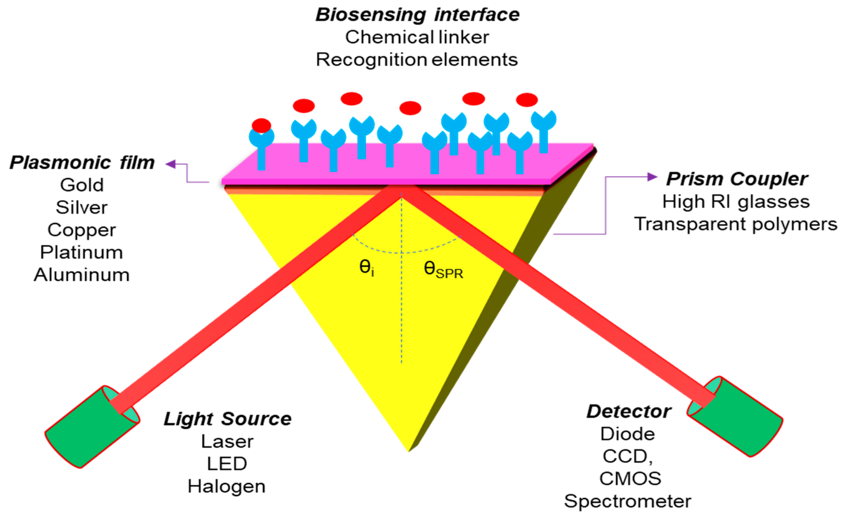
5.1. Metal Layer
5.2. 2D Material Layer
5.3. Selection of Glass Prism
5.4. Detection of SPR Sensor
6. SPR Application
6.1. SPR Biosensors
6.2. SPR Sensor for Food Quality and Safety
6.3. SPR Sensor for Material Characterization
6.4. SPR Sensor for the Study of the Physical Quantities
6.5. SPR as Chemical Sensor
7. Future Perspective of SPR Sensors
8. Commercial SPR Biosensors
9. Conclusions
Author Contributions
Acknowledgments
Conflicts of Interest
References
- Kelley, S.O.; Mirkin, C.A.; Walt, D.R.; Ismagilov, R.F.; Toner, M.; Sargent, E.H. Advancing the speed, sensitivity and accuracy of biomolecular detection using multi-length-scale engineering. Nat. Nanotechnol. 2014, 9, 969. [Google Scholar] [CrossRef]
- Sage, A.T.; Besant, J.D.; Lam, B.; Sargent, E.H.; Kelley, S.O. Ultrasensitive electrochemical biomolecular detection using nanostructured microelectrodes. Acc. Chem. Res. 2014, 19, 2417–2425. [Google Scholar] [CrossRef] [PubMed]
- Dai, Y.; Wu, Y.; Liu, G.; Gooding, J.J. CRISPR mediated biosensing toward understanding cellular biology and point-of-care diagnosis. Angew. Chem. 2020, 47, 2417–2425. [Google Scholar] [CrossRef]
- Dai, Y.; Furst, A.; Liu, C.C. Strand displacement strategies for biosensor applications. Trends Biotechnol. 2019, 37, 1367–1382. [Google Scholar] [CrossRef] [PubMed]
- Hajian, R.; Balderston, S.; Tran, T.; DeBoer, T.; Etienne, J.; Sandhu, M.; Wauford, N.A.; Chung, J.Y.; Nokes, J.; Athaiya, M.; et al. Detection of unamplified target genes via CRISPR–Cas9 immobilized on a graphene field-effect transistor. Nat. Biomed. Eng. 2019, 3, 427–437. [Google Scholar] [CrossRef]
- Gordon, J.G.; Ernst, S. Surface plasmons as a probe of the electrochemical interface. Int. J. Surf. Sci. 1980, 101, 499–506. [Google Scholar] [CrossRef]
- Wood, R.W. On a remarkable case of uneven distribution of light in a diffraction grating spectrum. Philos. Mag. Ser. 1902, 4, 396–402. [Google Scholar] [CrossRef]
- Turbadar, T. Complete absorption of light by thin film metal films. Proc. Phys. Soc. Lond. 1959, 469, 40–44. [Google Scholar] [CrossRef]
- Stewart, M.E.; Anderton, C.R.; Thompson, L.B.; Maria, J.; Gray, S.K.; Rogers, J.A.; Nuzzo, R.G. Nanostructured plasmonic sensors. Chem. Rev. 2008, 108, 494–521. [Google Scholar] [CrossRef]
- Liedberg, B.; Nylander, C.; Lundstrom, I. Surface plasmons resonance for gas detection and biosensing. Sens. Actuators 1983, 4, 299–304. [Google Scholar] [CrossRef]
- Zynio, S.A.; Samoylov, A.V.; Surovtseva, E.R.; Mirsky, V.M.; Shirshov, Y.M. Bimetallic layers increase sensitivity of affinity sensors based on surface plasmon resonance. Sensors 2002, 2, 62–70. [Google Scholar] [CrossRef]
- Berger, C.E.; Beumer, T.A.; Kooyman, R.P.; Greve, J. Surface plasmon resonance multisensing. Anal. Chem. 1998, 70, 703–706. [Google Scholar] [CrossRef]
- Peiris, S.; McMurtrie, J.; Zhu, H.-Y. Metal nanoparticle photocatalysts: Emerging processes for green organic synthesis. Catal. Sci. Technol. 2016, 6, 320–338. [Google Scholar] [CrossRef]
- Peterlinz, K.A.; Georgiadis, R.M.; Herne, T.M.; Tarlov, M.J. Observation of Hybridization and Dehybridization of Thiol-Tethered DNA Using Two-Color Surface Plasmon Resonance Spectroscopy. J. Am. Chem. Soc. 1997, 119, 3401–3402. [Google Scholar] [CrossRef]
- Koncki, R.; Mascini, M. Screen-printed ruthenium dioxide electrodes for pH measurements. Anal. Chim. Acta 1997, 351, 143–149. [Google Scholar] [CrossRef]
- Homola, J.; Yee, S.S.; Gauglitz, G. Surface plasmon resonance sensors: Review. Actuators 1999, 54, 3–15. [Google Scholar] [CrossRef]
- Homola, J. Present and future of surface plasmon resonance biosensor. Anal. Bioanal. Chem. 2003, 377, 528–539. [Google Scholar] [CrossRef]
- Willets, K.A.; van Duyne, R.P. Localized Surface Plasmon Resonance Spectroscopy and Sensing. Annu. Rev. Phys. Chem. 2007, 58, 267. [Google Scholar] [CrossRef]
- Myers, F.B.; Lee, L.P. Innovations in optical microfluidic technologies for point-of-care diagnostics. Lab Chip 2008, 8, 2015–2031. [Google Scholar] [CrossRef]
- Wang, K.; Zheng, Z.; Su, Y.L.; Wang, Z.Y.; Song, L.S.; Zhu, J.S. Hybrid differential interrogation method for sensitive surface plasmon resonance measurement enabled by electro-optically tunable SPR sensors. Opt. Express 2009, 17, 4468. [Google Scholar] [CrossRef]
- Mayer, K.M.; Hafner, J.H. Localized Surface Plasmon Resonance Sensors. Chem. Rev. 2011, 111, 3828. [Google Scholar] [CrossRef] [PubMed]
- Abdulhalim, I.; Zourob, M.; Lakhtakia, A. Surface Plasmon Resonance for Biosensing: A Mini Review. Electromagnetics 2008, 28, 214. [Google Scholar] [CrossRef]
- Haes, A.J.; van Duyne, R.P. A unified view of propagating and localized surface plasmon resonance biosensors. Anal. Bioanal. Chem. 2004, 379, 920. [Google Scholar] [CrossRef] [PubMed]
- Yeatman, E.M. Resolution and sensitivity in surface plasmon microscopy and sensing. Biosens. Bioelectron. 1996, 11, 635–649. [Google Scholar] [CrossRef]
- Kolomenskii, A.A.; Gershon, P.D.; Schuessler, H.A. Sensitivity and detection limit of concentration and adsorption measurements by laser-induced surface-plasmon resonance. Appl. Opt. 1997, 6539–6547. [Google Scholar] [CrossRef]
- McDonnell, J.M. Surface plasmon resonance: towards an understanding of the mechanisms of biological molecular recognition. Curr. Opin. Chem. Biol. 2001, 5, 572–577. [Google Scholar] [CrossRef]
- Naimushin, A.N.; Soelberg, S.D.; Nguyen, D.K.; Dunlap, L.; Bartholomew, D.; Elkind, J.; Melendez, J.; Furlong, C.E. Detection of Staphylococcus aureus enterotoxin B at femtomolar levels with a miniature integrated two-channel surface plasmon resonance (SPR) sensor. Biosens. Bioelectron. 2002, 17, 573–584. [Google Scholar] [CrossRef]
- Zeng, S.W.; Yu, X.; Law, W.C.; Zhang, Y.; Hu, R.; Dinh, X.Q.; Ho, H.P.; Yong, K.T. Size dependence of Au NP-enhanced surface plasmon resonance based on differential phase measurement. Sens. Actuators 2013, 176, 1128–1133. [Google Scholar] [CrossRef]
- Otto, A. Excitation of non-radiative surface plasma waves in silver by the method of frustrated total reflection. Int. J. Z. Phys. 1968, 216, 398–410. [Google Scholar] [CrossRef]
- Kretschmann, E.; Reather, H. Radiative decay of non-radiative surface plasmons excited by light. Z. Naturforsch. 1968, 23, 2135–2136. [Google Scholar] [CrossRef]
- Geim, A.K.; Novoselov, K.S. The rise of graphene. Nat. Mater. 2007, 6, 183–191. [Google Scholar] [CrossRef] [PubMed]
- Zhu, C.; Zeng, Z.; Li, H. Single-layer MoS2-based nanoprobes for homogeneous detection of biomolecules. J. Am. Chem. Soc. 2013, 135, 5998–6001. [Google Scholar] [CrossRef] [PubMed]
- Chernikov, A.; Berkelbach, T.C.; Hill, H.M.; Rigosi, A.; Li, Y.; Aslan, O.B.; Heinz, T.F. Exciton binding energy and nonhydrogenic Rydberg series in monolayer WS2. Phys. Rev. Lett. 2014, 113, 076802. [Google Scholar] [CrossRef] [PubMed]
- Kabashin, A.V.; Patskovsky, S.; Grigorenko, A.N. Phase and amplitude sensitivities in surface plasmon resonance bio and chemical sensing. Opt. Express 2009, 17, 21191–21204. [Google Scholar] [CrossRef] [PubMed]
- Li, T.; Galli, G. Electronic properties of MoS2 nanoparticles. J. Phys. Chem. C 2007, 111, 16192–16196. [Google Scholar] [CrossRef]
- Lebegue, S.; Eriksson, O. Electronic structure of two-dimensional crystals from ab initio theory. Phys. Rev. B 2009, 79, 115409. [Google Scholar] [CrossRef]
- Cheiwchanchamnangij, T.; Lambrecht, W.R.L. Quasiparticle band structure calculation of monolayer, bilayer, and bulk MoS2. Phys. Rev. 2012, 85, 205302. [Google Scholar] [CrossRef]
- Xiao, D.; Yao, W.; Niu, Q. Valley-contrasting physics in graphene: Magnetic moment and topological transport. Phys. Rev. Lett. 2007, 99, 236809. [Google Scholar] [CrossRef]
- Liu, G.B.; Shan, W.Y.; Yao, Y.; Yao, W.; Xiao, D. Three-band tight-binding model for monolayers of group-VIB transition metal dichalcogenides. Phys. Rev. 2013, 88, 085433. [Google Scholar] [CrossRef]
- He, K.; Kumar, N.; Zhao, L.; Wang, Z.; Mak, K.F.; Zhao, H.; Shan, J. Tightly bound excitons in monolayer WSe2. Phys. Rev. Lett. 2014, 113, 026803. [Google Scholar] [CrossRef]
- Shankaran, D.R.; Gobi, K.V.; Sakai, T.; Matsumoto, K.; Toko, K.; Miura, N. Surface plasmon resonance immunosensor for highly sensitive detection of 2,4,6-trinitrotoluene. Biosens. Bioelectron. 2005, 20, 1750–1756. [Google Scholar] [CrossRef] [PubMed]
- Igor, V. Bondarev and Maria R. Vladimirova, Optical generation of excitonic valley coherence in monolayer WSe2. Nat. Nanotech. 2013, 8, 634–638. [Google Scholar] [CrossRef]
- Mak, K.F.; McGill, K.L.; Park, J.; McEuen, P.L. The valley Hall effect in MoS2 transistors. Science 2014, 344, 1489–1499. [Google Scholar] [CrossRef] [PubMed]
- Gorbachev, R.V.; Song, J.C.W.; Yu, G.L.; Kretinin, A.V.; Withers, F.; Cao, Y.; Geim, A.K. Detecting topological currents in graphene superlattices. Science 2014, 346, 448–451. [Google Scholar] [CrossRef] [PubMed]
- Ramasubramaniam, A. Large excitonic effects in monolayers of molybdenum and tungsten dichalcogenides. Phys. Rev. 2012, 86, 115409. [Google Scholar] [CrossRef]
- Komsa, H.-P.; Krasheninnikov, A.V. Effects of confinement and environment on the electronic structure and exciton binding energy of MoS2 from first principles. Phys. Rev. 2012, 86, 241201. [Google Scholar] [CrossRef]
- Berkelbach, T.C.; Hybertsen, M.S.; Reichman, D.R. Theory of neutral and charged excitons in monolayer transition metal dichalcogenides. Phys. Rev. 2013, 88, 045318. [Google Scholar] [CrossRef]
- Qiu, D.Y.; da Jornada, F.H.; Louie, S.G. Optical spectrum of MoS2: Many body effects and diversity of exciton states. Phys. Rev. Lett. 2013, 111, 216805. [Google Scholar] [CrossRef]
- Mak, K.F.; He, K.; Lee, C.; Lee, G.H.; Hone, J.; Heinz, T.F.; Shan, J. Tightly bound trions in monolayer MoS2. Nat. Mater. 2013, 12, 207–211. [Google Scholar] [CrossRef]
- Ugeda, M.M.; Bradley, A.J.; Shi, S.F.; Felipe, H.; Zhang, Y.; Qiu, D.Y.; Wang, F. Giant bandgap renormalization and excitonic effects in a monolayer transition metal dichalcogenide semiconductor. Nat. Mater. 2014, 13, 1091–1095. [Google Scholar] [CrossRef]
- Rizal, C. Magneto-Optic Surface Plasmon Resonance Ti/Au/Co/Au/Pc Configuration and Sensitivity. Magnetochemistry 2018, 4, 35. [Google Scholar] [CrossRef]
- Lensky, Y.D.; Song, J.C.W.; Samutpraphoot, P.; Levitov, L.S. Topological valley currents in gapped Dirac materials. Phys. Rev. Lett. 2015, 114, 256601. [Google Scholar] [CrossRef] [PubMed]
- Ross, J.S.; Wu, S.; Yu, H.; Ghimire, N.J.; Jones, A.M.; Aivazian, G.; Xu, X. Electrical control of neutral and charged excitons in a monolayer semiconductor. Nat. Commu. 2013, 4, 1–6. [Google Scholar] [CrossRef]
- Shang, J.; Shen, X.; Cong, C.; Peimyoo, N.; Cao, B.; Eginligil, M.; Yu, T. Observation of excitonic fine structure in a 2D transition-metal dichalcogenide semiconductor. ACS Nano 2015, 9, 647–655. [Google Scholar] [CrossRef] [PubMed]
- You, Y.; Zhang, X.X.; Berkelbach, T.C.; Hybertsen, M.S.; Reichman, D.R.; Heinz, T.F. Observation of biexcitons in monolayer WSe2. Nat. Phys. 2015, 11, 477–481. [Google Scholar] [CrossRef]
- Sanvitto, D.; Pulizzi, F.; Shields, A.J.; Christianen, P.C.; Holmes, S.N.; Simmons, M.Y.; Ritchie, D.A.; Maan, J.C.; Pepper, M. Observation of charge transport by negatively charged excitons. Science 2001, 294, 837–839. [Google Scholar] [CrossRef] [PubMed]
- Xia, F.; Wang, H.; Xiao, D.; Dubey, M.; Ramasubramaniam, A. Twodimensional material nanophotonics. Nat. Photon. 2014, 8, 899–907. [Google Scholar] [CrossRef]
- Geim, A.K.; Grigorieva, I.V. Van der Waals heterostructures. Nature 2013, 499, 419–425. [Google Scholar] [CrossRef]
- Butler, S.Z.; Hollen, S.M.; Cao, L.; Cui, Y.; Gupta, J.A.; Gutiérrez, H.R.; Johnston-Halperin, E. Progress, challenges, and opportunities in two-dimensional materials beyond graphene. ACS Nano 2013, 7, 2898–2926. [Google Scholar] [CrossRef]
- Xiao, D.; Chang, M.-C.; Niu, Q. Berry phase effects on electronic properties. Rev. Mod. Phys. 2010, 82, 1959–2007. [Google Scholar] [CrossRef]
- Koppens, F.H.L.; Mueller, T.; Avouris, P.; Ferrari, A.C.; Vitiello, M.S.; Polini, M. Photodetectors based on graphene, other twodimensional materials and hybrid systems. Nat. Nanotech. 2014, 9, 780–793. [Google Scholar]
- Srivastava, A.; Sidler, M.; Allain, A.V.; Lembke, D.S.; Kis, A.; Imamoğlu, A. Valley Zeeman effect in elementary optical excitations of monolayer WSe2. Nat. Phys. 2015, 11, 141–147. [Google Scholar] [CrossRef]
- MacNeill, D.; Heikes, C.; Mak, K.F.; Anderson, Z.; Kormányos, A.; Zólyomi, V.; Park, J.; Ralph, D.C. Breaking of valley degeneracy by magnetic field in monolayer MoSe2. Phys. Rev. Lett. 2015, 114, 037401. [Google Scholar] [CrossRef] [PubMed]
- Li, Y.; Ludwig, J.; Low, T.; Chernikov, A.; Cui, X.; Arefe, G.; Heinz, T.F. Valley splitting and polarization by the Zeeman effect in monolayer MoSe2. Phys. Rev. Lett. 2014, 113, 266804. [Google Scholar] [CrossRef] [PubMed]
- Aivazian, G.; Gong, Z.; Jones, A.M.; Chu, R.L.; Yan, J.; Mandrus, D.G.; Xu, X. Magnetic control of valley pseudospin in monolayer WSe2. Nat. Phys. 2015, 11, 148–152. [Google Scholar] [CrossRef]
- Cao, T.; Wang, G.; Han, W.; Ye, H.; Zhu, C.; Shi, J.; Feng, J. Valley-selective circular dichroism of monolayer molybdenum disulphide. Nat. Commun. 2012, 3, 1–5. [Google Scholar] [CrossRef]
- Mak, K.F.; He, K.; Shan, J.; Heinz, T.F. Control of valley polarization in monolayer MoS2 by optical helicity. Nat. Nanotech. 2012, 7, 494–498. [Google Scholar] [CrossRef]
- Zeng, H.; Dai, J.; Yao, W.; Xiao, D.; Cui, X. Valley polarization in MoS2 monolayers by optical pumping. Nat. Nanotech. 2012, 7, 490–493. [Google Scholar] [CrossRef]
- Sallen, G.; Bouet, L.; Marie, X.; Wang, G.; Zhu, C.R.; Han, W.P.; Urbaszek, B. Robust optical emission polarization in MoS2 monolayers through selective valley excitation. Phys. Rev. 2012, 86, 081301. [Google Scholar] [CrossRef]
- Prabowo, B.A.; Alom, A.; Secario, M.K.; Masim, F.C.P.; Lai, H.C.; Hatanaka, K.; Liu, K.C. Graphene-based portable SPR sensor for the detection of Mycobacterium tuberculosis DNA strain. Procedia Eng. 2016, 168, 541–545. [Google Scholar] [CrossRef]
- Nelson, S.; Johnston, K.; Yee, S. High sensitivity surface plasmon resonace sensor based on phase detection. Sens. Actuators B Chem. 1996, 35, 187–191. [Google Scholar] [CrossRef]
- Kim, S.J.; Gobi, K.V.; Harada, R.; Shankaran, D.R.; Miura, N. Miniaturized portable surface plasmon resonance immunosensor applicable for on-site detection of low-molecular-weight analytes. Sens. Actuators B Chem. 2006, 115, 349–356. [Google Scholar] [CrossRef]
- Wang, G.; Marie, X.; Gerber, I.; Amand, T.; Lagarde, D.; Bouet, L.; Urbaszek, B. Giant enhancement of the optical second-harmonic emission of WSe2 monolayers by laser excitation at exciton resonances. Phys. Rev. Lett. 2015, 114, 097403. [Google Scholar] [CrossRef] [PubMed]
- Chiu, N.F.; Fan, S.Y.; Yang, C.D.; Huang, T.Y. Carboxyl-functionalized graphene oxide composites as SPR biosensors with enhanced sensitivity for immunoaffinity detection. Biosens. Bioelectron. 2017, 89, 370–376. [Google Scholar] [CrossRef]
- Narsaiah, K.; Jha, S.N.; Bhardwaj, R.; Sharma, R.; Kumar, R. Optical biosensors for food quality and safety assurance—A review. J. Food Sci. Technol. 2011, 49, 383–406. [Google Scholar] [CrossRef]
- Cudazzo, P.; Tokatly, I.V.; Rubio, A. Dielectric screening in two-dimensional insulators: Implications for excitonic and impurity states in graphane. Phys. Rev. 2011, 84, 085406. [Google Scholar] [CrossRef]
- Sepúlveda, B.; Calle, A.; Lechuga, L.M.; Armelles, G. Highly sensitive detection of biomolecules with the magneto-optic surface-plasmon-resonance sensor. Opt. Lett. 2006, 31, 1085. [Google Scholar] [CrossRef]
- Walsh, L.A.; Addou, R.; Wallace, R.M.; Hinkle, C.L. Molecular Beam Epitaxy of Transition Metal Dichalcogenides. Mol. Beam Ep. 2018, 515–531. [Google Scholar] [CrossRef]
- Abraha, K.; Bambang Setio Utomo, A. Computational Study of Sensitivity Enhancement in Surface Plasmon Resonance (SPR) Biosensors by Using the Inclusion of the Core-Shell for Biomaterial Sample Detection. Biosensors 2018, 8, 75. [Google Scholar] [CrossRef]
- Hamola, J. Electromagnetic theory of surface plasmons. Springer Ser Chem. Sens. Biosen. 2006, 4, 3–44. [Google Scholar]
- Gauglitz, G.; Moore, D.S. Handbook of Spectroscopy; Wiley VCH: Weinheim, Germany, 2014. [Google Scholar]
- Lyon, L.A.; Musick, M.D.; Natan, M.J. Colloidal Au-Enhanced Surface Plasmon Resonance Immunosensing. Anal. Chem. 1999, 70, 5177–5183. [Google Scholar] [CrossRef] [PubMed]
- Wang, J.L.; Munir, A.; Li, Z.H.; Zhou, H.S. Aptamer-Au NPs conjugates-enhanced SPR sensing for the ultrasensitive sandwich immunoassay. Biosens. Bioelectron. 2009, 25, 124–129. [Google Scholar] [CrossRef] [PubMed]
- Chou, C.-H.; Chen, F.-C. Plasmonic nanostructures for light trapping in organic photovoltaic devices. Nanoscale 2014, 6, 8444–8458. [Google Scholar] [CrossRef] [PubMed]
- Gupta, B.D.; Verma, R.K. Surface plasmon resonance-based fiber optic sensors: Principle, probe designs, and some applications. J. Sens. 2009, 2009, 1–12. [Google Scholar] [CrossRef]
- Sharma, A.K.; Gupta, B.D. Metal–semiconductor nano composite layer based optical fibre surface plasmon resonance sensor. J. Opt. A Pure Appl. Opt. 2007, 9, 180–185. [Google Scholar] [CrossRef]
- Sharma, A.K.; Jha, R.; Pattanaik, H.S. Design considerations for surface plasmon resonance-based detection of human blood group in near infrared. J. Appl. Phys. 2010, 107, 1–6. [Google Scholar] [CrossRef]
- Bruna, M.; Borini, S. Optical constants of graphene layers in the visible range. Appl. Phys. Lett. 2009, 94, 031901. [Google Scholar] [CrossRef]
- Gupta, B.D.; Sharma, A.K. Sensitivity evaluation of a multi-layered surface plasmon resonance-based fibre optic sensor: A theoretical study. Sens. Actuators B Chem. 2005, 107, 40–46. [Google Scholar] [CrossRef]
- Maurya, J.; Prajapati, Y.; Singh, V.; Saini, J.; Tripathi, R. Performance of graphene–MoS2 based surface plasmon resonance sensor using Silicon layer. Opt. Quantum Electron. 2015, 47, 3599–3611. [Google Scholar] [CrossRef]
- Schott Optical Glass Data Sheets. Available online: http://refractiveindex.info (accessed on 25 May 2020).
- Xie, J.; Zhang, D.; Yan, X.Q.; Ren, M.; Zhao, X.; Liu, F.; Sun, R.; Li, X.; Li, Z.; Chen, S.; et al. Optical properties of chemical vapor deposition-grown PtSe2 characterized by spectroscopic ellipsometry. Mater 2019, 6, 035011. [Google Scholar] [CrossRef]
- Rahman, M.S.; Anower, M.K.; Rahman, M.R.; Hasan, M.B.; Hossain, M.; Haque, M.I. Modeling of a highly sensitive MoS2-Graphene hybrid-based fiber optic SPR biosensor for sensing DNA hybridization. Optik 2017, 140, 989–997. [Google Scholar] [CrossRef]
- Maharana, P.K.; Jha, R. Chalcogenide prism and graphene multilayer based surface plasmon resonance a_nity biosensor for high performance. Sens. Actuators B Chem. 2012, 169, 161–166. [Google Scholar] [CrossRef]
- Homola, J. Surface plasmon resonance sensors for detection of chemical and biological species. Chem. Rev. 2008, 108, 462–493. [Google Scholar] [CrossRef] [PubMed]
- Ramanujam, J.; Singh, U.P. Copper indium gallium selenide based solar cells–a review. Energy Environ. Sci. 2017, 10, 1306–1319. [Google Scholar] [CrossRef]
- Fotovvati, B.; Namdari, N.; Dehghanghadikolaei, A. On coating techniques for surface protection: A review. J. Manuf. Mater. Process. 2019, 3, 28. [Google Scholar] [CrossRef]
- Weber, W.H.; McCarthy, S.L. Surface-plasmon resonance as a sensitive optical probe of metal-film properties. Phys. Rev. 1975, 12, 5643–5650. [Google Scholar] [CrossRef]
- Ordal, M.A.; Long, L.L.; Bell, R.J.; Bell, S.E.; Bell, R.R.; Alexander, R.W.; Ward, C.A. Optical properties of the metals Al, Co, Cu, Au, Fe, Pb, Ni, Pd, Pt, Ag, Ti, and W in the infrared and far infrared. Appl. Opt. 1983, 22, 1099–1119. [Google Scholar] [CrossRef] [PubMed]
- Sadowski, J.W.; Lekkala, J.; Vikholm, I. Biosensors based on surface plasmons excited in non-noble metals. Biosens. Bioelectron. 1991, 6, 439–444. [Google Scholar] [CrossRef]
- Sharma, A.K. Performance of different metals in optical fiber-based surface plasmon resonance sensor. Pramana J. Phys. Indian Acad. Sci. 2012, 78, 417–427. [Google Scholar] [CrossRef]
- Nesterenko, D.V.; Rehman, S.; Sekkat, Z. Surface plasmon sensing with different metals in single double layer configuration. Int. J. Appl. Opt. 2012, 51, 6673–6682. [Google Scholar] [CrossRef]
- Lavers, C.R.; Wilkinson, J.S. A waveguide coupled surface plasmon sensor for an aqueous enviourment. Int. J. Sci. Actuators B 1994, 22, 75–81. [Google Scholar] [CrossRef]
- Tyroky, J.C.; Homola, J.; Skalsky, M. Tuning of spectral operation range of a waveguide surface plasmon resonance sensor. Int. J. Electron. Lett. 1997, 33, 1246–1248. [Google Scholar]
- Weiss, M.N.; Srivastava, R.; Groger, H. Experimental investigation of a surface plasmon based integrated optic humidity sensor. Int. J. Electron. Lett. 1996, 32, 842–843. [Google Scholar] [CrossRef]
- Maurya, J.B.; François, A.; Prajapati, Y.K. Two-dimensional layered nanomaterial-based one-dimensional photonic crystal refractive index sensor. Sensors 2018, 18, 857. [Google Scholar] [CrossRef] [PubMed]
- Xia, J.; Huang, X.; Liu, L.Z.; Wang, M.; Wang, L.; Huang, B.; Zhu, D.D.; Li, J.J.; Gu, C.Z.; Meng, X.M. CVD synthesis of large-area, highly crystalline MoSe2 atomic layers on diverse substrates and application to photodetectors. Nanoscale 2014, 6, 8949–8955. [Google Scholar] [CrossRef] [PubMed]
- Sreekanth, K.V.; Zeng, S.; Shang, J.Z.; Yong, K.T.; Yu, T. Excitation of surface electromagnetic waves in a graphene-based Bragg grating. Sci Rep. 2012, 2, 737. [Google Scholar] [CrossRef]
- Zeng, S.; Baillargeat, D.; Ho, H.P.; Yong, K.T. Nanomaterials enhanced surface plasmon resonance for biological and chemical sensing applications. Chem. Soc. Rev. 2014, 43, 3426–3452. [Google Scholar] [CrossRef]
- Eda, G.; Maier, S.A. Two-dimensional crystals: Managing light for optoelectronics. ACS Nano 2013, 7, 5660–5665. [Google Scholar] [CrossRef]
- Zeng, S.; Hu, S.; Xia, J.; Anderson, T.; Dinh, X.Q.; Meng, X.M.; Coquet, P.; Yong, K.T. Graphene-MoS2 hybrid nanostructures enhanced surface plasmon resonance biosensors. Sens. Actuators B Chem. 2015, 207, 801–810. [Google Scholar] [CrossRef]
- Wu, L.; Jia, Y.; Jiang, L.; Guo, J.; Dai, X.; Xiang, Y.; Fan, D. Sensitivity improved SPR biosensor based on the MoS2/ graphene-aluminum hybrid structure. J. Lightwave Technol. 2017, 35, 82–87. [Google Scholar] [CrossRef]
- Wu, L.; Guo, J.; Wang, Q.; Lu, S.; Dai, X.; Xiang, Y.; Fan, D. Sensitivity enhancement by using few-layer black phosphorus graphene/TMDCs heterostructure in surface plasmon resonance biochemical sensor. Sens. Actuators B Chem. 2017, 249, 542–548. [Google Scholar] [CrossRef]
- Wu, L.; Chu, H.S.; Koh, W.S.; Li, E.P. Highly sensitive graphene biosensors based on surface plasmon resonance. Opt. Express 2010, 18, 14395–14400. [Google Scholar] [CrossRef] [PubMed]
- Li, Y.; Chernikov, A.; Zhang, X.; Rigosi, A.; Hill, H.M.; van der Zande, A.M.; Chenet, D.A.; Shih, E.M.; Hone, J.; Heinz, T.F. Measurement of the optical dielectric function of monolayer transition-metal dichalcogenides: MoS2, MoSe2, WS2, and WSe2. Phys. Rev. B 2014, 90, 205–422. [Google Scholar] [CrossRef]
- Zhao, X.; Huang, T.; Ping, P.S.; Wu, X.; Huang, P.; Pan, J.; Wu, Y.; Cheng, Z. Sensitivity enhancement in surface plasmon resonance biochemical sensor based on transition metal dichalcogenides/graphene heterostructure. Sensors 2018, 18, 2056. [Google Scholar] [CrossRef]
- Kooyman, R.P.H. Handbook of surface plasmon resonance. R. Soc. Chem. 2008, 2, 15–34. [Google Scholar]
- Regatos, D.; Sepúlveda, B.; Fariña, D.; Carrascosa, L.G.; Lechuga, L.M. Suitable combination of noble/ferromagnetic metal multilayers for enhanced magneto-plasmonic biosensing. Opt. Express 2011, 19, 8336. [Google Scholar] [CrossRef]
- Zhang, N.; Humbert, G.; Gong, T.; Shum, P.P.; Li, K.; Auguste, J.L.; Wu, Z.; Hu, J.; Feng, L.; Dinh, Q.X.; et al. Side-channel photonic crystal fiber for surface enhanced Raman scattering sensing. Sens. Actuators B Chem. 2016, 233, 195–201. [Google Scholar] [CrossRef]
- Seifouri, M.; Rouini, M.A.; Olyaee, S. A Photonic Crystal Fiber Based Surface Plasmon Resonance Biosensor with Elliptical and Circular Holes. J. Nanoelectron. Optoelectron. 2019, 14, 335–341. [Google Scholar] [CrossRef]
- Situ, C.; Mooney, M.H.; Elliott, C.T.; Buijs, J. Advances in surface plasmon resonance biosensor technology towards high-throughput, food-safety analysis. Trends Anal. Chem. 2010, 29, 1305–1315. [Google Scholar] [CrossRef]
- Verma, R.; Gupta, B.D.; Jha, R. Sensitivity enhancement of a surface plasmon resonance-based biomolecules sensor using graphene and silicon layers. Sens. Actuators B Chem. 2011, 160, 623–631. [Google Scholar] [CrossRef]
- Verma, A.; Prakash, A.; Tripathi, R. Performance analysis of graphene-based surface plasmon resonance biosensors for detection of pseudomonas-like bacteria. Opt. Quantum Electron. 2014, 47, 1197–1205. [Google Scholar] [CrossRef]
- Mishra, A.K.; Mishra, S.K. An SPR-based sensor with an extremely large dynamic range of refractive index measurements in the visible region. J. Phys. D Appl. Phys. 2015, 48, 435502. [Google Scholar] [CrossRef]
- Ouyang, Q.; Zeng, S. Sensitivity enhancement of transition metal dichalcogenides/silicon nano structure-based surface plasmon resonance biosensor. Sci. Rep. 2016, 6, 28190. [Google Scholar] [CrossRef] [PubMed]
- Lin, Z.; Jiang, L. Tuning and sensitivity enhancement of surface plasmon resonance biosensor with graphene covered Au–MoS2–Au films. IEEE Photonics J. 2016, 8, 1–8. [Google Scholar] [CrossRef]
- Pal, S.; Verma, A.; Prajapati, Y. Influence of black phosphorous on performance of SPR biosensor. Opt. Quant. Electron. 2017, 49, 403. [Google Scholar] [CrossRef]
- Shushama, K.N.; Rana, M.M.; Inum, R.; Hossain, M.B. Sensitivity enhancement of graphene coated surface plasmon resonance biosensor. Opt. Quant Electron. 2017, 49, 381. [Google Scholar] [CrossRef]
- Saifur, R.; Rabiul, H.; Khaleda, A.R.; Anowera, M. A novel graphene coated SPR biosensor with WS2 for DNA hybridization. Opt. Mater. 2018, 75, 567–573. [Google Scholar]
- Saifur, R.; Shamim, A.; Rabiul, H.; Biplob, M. Design and numerical analysis of highly sensitive Au-MoS2-graphene based hybrid surface plasmon resonance biosensor. Opt. Commun. 2017, 396, 36–43. [Google Scholar]
- Akash, Y.K. Performance analysis of silicon and blue phosphorene-MoS2 hetro structure based SPR sensor. Photonic Sens. 2019, 9, 284–292. [Google Scholar] [CrossRef]
- Nisha, A.; Maheswari, P.; Anbarasan, P.M.; Rajesh, K.B.; Jaroszewicz, Z. Sensitivity enhancement of surface plasmon resonance sensor with 2D material covered noble and magnetic material (Ni). Opt. Quantum Electron. 2019, 51, 19. [Google Scholar] [CrossRef]
- Moznuzzaman, M.; Rafiqul, I.; Biplob, H.; Ibrahim, M. Modeling of highly improved spr sensor for formalin detection. Results Phys. 2020, 16, 102874. [Google Scholar] [CrossRef]
- Tanabe, I.; Tanaka, Y.Y.; Ryoki, T.; Watari, K.; Goto, T.; Kikawada, M.; Inami, W.; Kawata, Y.; Ozaki, Y. Direct optical measurements of far-and deep-ultraviolet surface plasmon resonance with different refractive indices. Opt. Express 2016, 24, 21886–21896. [Google Scholar] [CrossRef] [PubMed]
- Tanabe, I.; Tanaka, Y.Y.; Hanulia, K.; Goto, T.; Inami, T.; Kawata, W.; Ozaki, Y. Recent Advances in Molecular Spectroscopy of Electronic and Vibrational Transitions in Condensed Phase and Its Application to Chemistry. Bull. Chem. Soc. Jpn. 2019, 92, 629–654. [Google Scholar] [CrossRef]
- Gupta, G.; Kondoh, J. Tuning and sensitivity enhancement of surface plasmon resonance sensor. Sens. Actuators 2007, 122, 381–388. [Google Scholar] [CrossRef]
- Sharma, K.P.A.; Basu, K.A. Fluoride glass-based surface plasmon resonance sensor in infrared region: Performance evaluation. Phys. D Appl. Phys. 2017, 50, 185103. [Google Scholar]
- Gupta, G.; Sugimoto, M.; Matsui, Y.; Kondoh, J. Use of a low refractive index prism in surface plasmon resonance biosensing. Sens. Actuators 2008, 130, 689–695. [Google Scholar] [CrossRef]
- Obreja, P.; Cristea, D.; Kusko, M. Dinescu, Surface plasmon resonance: Material and interface design for universal accessibility. Opt. A Pure Appl. Opt. 2008, 10. [Google Scholar]
- Lan, G.Q.; Liu, S.G.; Zhang, X.R.; Wang, Y.X.; Song, Y.L. Applications of graphene and related nanomaterials in analytical chemistry. Rev. Sci. Instrum. 2015, 86. [Google Scholar] [CrossRef]
- Prabowo, B.A.; Purwidyantri, A.; Liu, K.C. Surface plasmon resonance optical sensor: A review on light source technology. Biosensors 2018, 8, 80. [Google Scholar] [CrossRef]
- Lan, G.Q.; Liu, S.G.; Ma, Y.; Zhang, X.R.; Wang, Y.X.; Song, Y.L. Sensitivity and figure-of-merit enhancements of liquid-prism SPR sensor in the angular interrogation. Opt. Commun. 2015, 352, 49–54. [Google Scholar] [CrossRef]
- Labib, M.; Sargent, E.H.; Kelley, S.O. Electrochemical methods for the analysis of clinically relevant biomolecules. Chem. Rev. 2016, 116, 9001–9090. [Google Scholar] [CrossRef] [PubMed]
- Dai, Y.; Liu, C.C. Recent advances on electrochemical biosensing strategies toward universal point-of-care systems. Angew. Chem. 2019, 131, 12483–12496. [Google Scholar] [CrossRef]
- Kim, J.; Campbell, A.S.; de Ávila, B.E.; Wang, J. Wearable biosensors for healthcare monitoring. Nat. Biotechnol. 2019, 37, 389–406. [Google Scholar] [CrossRef] [PubMed]
- Gross, B.; Lockwood, S.Y.; Spence, D.M. Recent advances in analytical chemistry by 3D printing. Anal. Chem. 2017, 89, 57–70. [Google Scholar] [CrossRef]
- Kotz, F.; Arnold, K.; Bauer, W.; Schild, D.; Keller, N.; Sachsenheimer, K.; Nargang, T.M.; Richter, C.; Helmer, D.; Rapp, B.E. Three-dimensional printing of transparent fused silica glass. Nature 2017, 544, 337–339. [Google Scholar] [CrossRef] [PubMed]
- Shuaiwen, G.; Yuting, Z.; Xiaoya, D.; Yuanjiang, X. Sensitivity enhancement of surface plasmon resonance sensors with 2D franckeite nanosheets. Result Phys. 2019, 13, 102320. [Google Scholar]
- SaifurRahmana, M.; Riktaa, K.A.; Abdulrazakb, M.S. Enhanced performance of snse-graphene hybrid photonic surface plasmon refractive sensor for biosensing applications. Photonics Nanostructures Fundam. Appl. 2020. [Google Scholar]
- Yin, Z.; Li, H.; Li, H.; Jiang, L.; Shi, Y.; Sun, Y.; Zhang, H. Single-Layer MoS2 Phototransistors. ACS Nano 2011, 6, 74–80. [Google Scholar] [CrossRef]
- Xu, H.; Chen, J.; Birrenkott, J.; Zhao, J.X.; Takalkar, S.; Baryeh, K.; Liu, G. Gold-Nanoparticle-decorated silica nanorods for sensitive visual detection of proteins. Anal. Chem. 2014, 86, 7351–7359. [Google Scholar] [CrossRef]
- Xuyan, H.; Yuhong, Z.; Jingjing, N.; Songyin, Z.; Yaping, T.; Nandi, Z. Gold nanoparticle based photometric determination of tobramycin by using new specific DNA aptamers. Microchim. Acta 2018. [Google Scholar] [CrossRef]
- Zhang, J.; Atay, T.; Nurmikko, A.V. Optical detection of brain cell activity using plasmonic gold nanoparticles. Nano Lett. 2008, 9, 519–524. [Google Scholar] [CrossRef] [PubMed]
- Zhao, H.; Ivic, L.; Otaki, J.M.; Hashimoto, M.; Mikoshiba, K.; Firestein, S. Functional expression of a mammalian odorant receptor. Science 1998, 279, 237–242. [Google Scholar] [CrossRef] [PubMed]
- Granqvist, N.; Liang, H.; Laurila, T.; Sadowski, J.; Yliperttula, M.; Viitala, T. Characterizing ultrathin and thick organic layers by surface plasmon resonance three-wavelength and waveguide mode analysis. Langmuir 2013, 29, 8561–8571. [Google Scholar] [CrossRef] [PubMed]
- Vidic, J.M.; Grosclaude, J.; Persuy, M.-A.; Aioun, J.; Salesse, R.; Pajot-Augy, E. Quantitative assessment of olfactory receptors activity in immobilized nanosomes: a novel concept for bioelectronic nose. Lab Chip 2006, 6, 1026–1032. [Google Scholar] [CrossRef] [PubMed]
- Wetzel, C.H.; Oles, M.; Wellerdieck, C.; Kuczkowiak, M.; Gisselmann, G.; Hatt, H. Specificity and sensitivity of a human olfactory receptor functionally expressed in human embryonic kidney 293 cells andxenopus laevis oocytes. J. Neurosci. 1999, 19, 7426–7433. [Google Scholar] [CrossRef] [PubMed]
- Li, Y.-J.; Xiang, J.; Zhou, F. Sensitive and Label-Free Detection of DNA by Surface Plasmon Resonance. Plasmonics 2007, 2, 79–87. [Google Scholar] [CrossRef]
- Liang, H.; Miranto, H.; Granqvist, N.; Sadowski, J.W.; Viitala, T.; Wang, B.; Yliperttula, M. Surface plasmon resonance instrument as a refractometer for liquids and ultrathin films. Sens. Actuators B Chem. 2010, 149, 212–220. [Google Scholar] [CrossRef]
- CRC. Handbook of Chemistry and Physics; Lide, D.R., Ed.; CRC Press, Taylor & Francis Group: Oxfordshire, UK, 2007–2008. [Google Scholar]
- Junga, L.S.; Nelsonb, K.E.; Campbell, C.T.; Staytonb, P.S.; Yeec, S.S.; Pérez-Lunad, V.; Lópezd, G.P. Surface plasmon resonance measurement of binding and dissociation of wild-type and mutant streptavidin on mixed biotin-containing alkylthiolate monolayers. Sens. Actuators B Chem. 1999, 54, 137–144. [Google Scholar] [CrossRef]
- Mak, K.F.; Lee, C.; Hone, J.; Shan, J.; Heinz, T.F. Atomically thin MoS2: a new direct- Gap semiconductor. Phys. Rev. Lett. 2010, 105, 136805. [Google Scholar] [CrossRef]
- Krishnan, R.V.; Varma, R.; Mayor, S.J. Fluorescence methods to probe nanometer-scale organization of molecules in living cell membranes. J. Fluoresc. 2001, 11, 211–226. [Google Scholar] [CrossRef]
- Lazcka, O.; Del Campo, F.J.; Munoz, F.X. Pathogen detection: a perspective of traditional methods and biosensors. Biosens. Bioelectron. 2007, 22, 1205–1217. [Google Scholar] [CrossRef] [PubMed]
- Leary, S.C.; Hill, B.C.; Lyons, C.N.; Carlson, C.G.; Michaud, D.; Kraft, C.S.; Ko, K.; Glerum, D.M.; Moyes, C.D. Chronic treatment with azide in situ leads to an irreversible loss of cytochrome c oxidase activity via holoenzyme dissociation. J. Biol. Chem. 2002, 277, 11321–11328. [Google Scholar] [CrossRef] [PubMed]
- Liu, D.; Zhang, D.; Scafidi, J.; Wu, X.; Cramer, C.C.; Davis, A.E. C1 inhibitor prevents Gram-negative bacterial lipopolysaccharide-induced vascular permeability. Blood 2005, 105, 2350–2355. [Google Scholar] [CrossRef]
- Lord, M.S.; Modin, C.; Foss, M.; Duch, M.; Simmons, A.; Pedersen, F.S.; Besenbacher, F.; Milthorpe, B.K. Extracellular matrix remodelling during cell adhesion monitored by the quartz crystal microbalance. Biomaterials 2008, 29, 2581–2587. [Google Scholar] [CrossRef] [PubMed]
- Homola, J.; Slavı´k, R. Fibre-optic sensor based on surfaceplasmon resonance. Electron. Lett. 1996, 32, 480–482. [Google Scholar] [CrossRef]
- Srivastava, A.K.; Zyskind, J.L. Electrical characteristics of InAsSb/GaSb heterojunctions. Appl. Phys. Lett. 1986, 49, 41–43. [Google Scholar] [CrossRef]
- Liang, H.M.; Viitala, T.; Tuppurainen, J.; Yliperttula, M. Surface plasmon resonance (SPR) used for detecting the ordering of organic monolayer. Sens. Actuators B Chem. 2013, 50, 492–501. [Google Scholar]
- Tang, Y.; Mernaugh, R.; Zeng, X. Nonregeneration protocol for surface plasmon resonance: study of high-affinity interaction with high-density biosensors. Anal. Chem. 2006, 78, 1841–1848. [Google Scholar] [CrossRef][Green Version]
- Nguyen, B.; Tanious, F.A.; Wilson, W.D. Biosensor-surface plasmon resonance: Quantitative analysis of small molecule-nucleic acid interactions. Methods 2007, 42, 150–161. [Google Scholar] [CrossRef]
- Chadwick, B.; Gal, M. An optical temperature sensor using surface plasmons. Jpn. J. Appl. Phys. 1993, 32, 2716–2717. [Google Scholar] [CrossRef]
- Mišković, Z.L.; Upadhyaya, N. Modeling electrolytically top-gated grapheme. Nanoscale Res. Lett. 2010, 5, 505–511. [Google Scholar] [CrossRef]
- Zhan, T.; Shi, X.; Dai, Y.; Liu, X.; Zi, J. Transfer matrix method for optics in graphene layers. J. Phys. Condens. Matter 2013, 25, 215301. [Google Scholar] [CrossRef]
- Paivasaari, K.; Tikhomirov, V.K.; Turunen, J. High refractive index chalcogenide glass for photonic crystal applications. Opt. Exp. 2007, 15, 2336–2340. [Google Scholar] [CrossRef] [PubMed]
- Cao, C.; Kim, J.P.; Kim, B.W.; Chae, H.; Yoon, H.C.; Yang, S.S.; Sim, S.J. A strategy for sensitivity and specificity enhancements in prostate specific antigen-alpha1-antichymotrypsin detection based on surface plasmon resonance. Biosens. Bioelectron. 2006, 21, 2106–2113. [Google Scholar] [CrossRef] [PubMed]
- Wei, J.; Mu, Y.; Song, D.; Fang, X.; Liu, X.; Bu, L.; Jin, Q. A novel sandwich immunosensing method for measuring cardiac troponin I in sera. Anal. Biochem. 2003, 321, 209–216. [Google Scholar] [CrossRef]
- Fitzpatrick, B.; O’Kennedy, R. The development and application of a surface plasmon resonance-based inhibition immunoassay for the determination of warfarin in plasma ultrafiltrate. J. Immunol. Methods 2004, 291, 11–12. [Google Scholar] [CrossRef] [PubMed]
- Yang, C.-Y.; Brooks, E.; Li, Y.; Denny, P.; Ho, C.-M.; Qi, F.; Montemagno, C.D. Detection of picomolar levels of interleukin-8 in human saliva by SPR. Lab Chip 2005, 5, 1017. [Google Scholar] [CrossRef] [PubMed]
- Chung, J.W.; Bernhardt, R.R.; Pyun, J.C. Sequential analysis of multiple analytes using a surface plasmon resonance (SPR) biosensor. J. Immunol. Methods 2006, 311, 178–188. [Google Scholar] [CrossRef] [PubMed]
- Yu, P.Y.; Cardona, M. Fundamentals of Semiconductors, 4th ed.; Springer: Berlin, Germany, 2010. [Google Scholar]
- Haberer, D.V.V.D.; Vyalikh, D.V.; Taioli, S.; Dora, B.; Farjam, M.; Fink, J.; Dresselhaus, M.S. Tunable band gap in hydrogenated quasi-free-standing grapheme. Nano Lett. 2010, 10, 3360–3366. [Google Scholar] [CrossRef]
- Trevino, J.; Calle, A.; Rodriguez-Frade, J.M.; Mellado, M.; Lechuga, M. Surface plasmon resonance immunoassay analysis of pituitary hormones in urine and serum samples. Clin. Chim. Acta 2009, 403, 56–62. [Google Scholar] [CrossRef]
- O’Brien, M.; Lee, K.; Morrish, R.; Berner, N.C.; McEvoy, N.; Wolden, C.A.; Duesberg, G.S. Plasma assisted synthesis of WS2 for gas sensing applications. Chem. Phys. Lett. 2014, 615, 6–10. [Google Scholar] [CrossRef]
- Luo, Y.; Chen, C.; Xia, K.; Peng, S.; Guan, H.; Tang, J. Tungsten disulfide (WS 2) based allfiber-optic humidity sensor. Opt. Express 2016, 24, 8956–8966. [Google Scholar] [CrossRef] [PubMed]
- Reather, H. Surface plasmons on smooth and rough surfaces and on gratings. Springer Tracts Mod. Phys. 1988, 111, 1–3. [Google Scholar]
- Owen, V. Real-time optical immunosensors: A commercialreality. Biosensors. Bioelectron. 1997, 12, i–ii. [Google Scholar] [CrossRef]
- Lin, C.C.; Tseng, Z.L.; Chen, L.C. Contour-Mode ZnO-Based Thin-Film Bulk Acoustic-Wave Resonator for Humidity Sensor Applications. J. Nanoelectron. Optoelectronic. 2019, 14, 729–733. [Google Scholar] [CrossRef]
- Kullab, H.M.; Taya, S.A.; El-Agez, T.M. Metal-clad waveguide sensor using a left-handed material as a core layer. J. Opt. Soc. Am. 2012, 29, 959–964. [Google Scholar] [CrossRef]
- Saifur, R.; Shaikh, S.N.; Anower, M.S.; Lway, F.A.; Maksudur, R.M.; Rikta, K.A. Design and numerical analysis of a graphene-coated fiber-optic SPR biosensor using tungsten disulfide. Photonics Nanostructures Fundam. Appl. 2019. [Google Scholar] [CrossRef]
- Splendiani, A.; Sun, L.; Zhang, Y.; Li, T.; Kim, J.; Chim, C.Y.; Wang, F. Emerging photoluminescence in monolayer MoS2. Nano Lett. 2010, 10, 1271–1275. [Google Scholar] [CrossRef]
- Mak, K.F.; Shan, J. Photonics and optoelectronics of 2D semiconductor transition metal dichalcogenides. Nat. Photonics 2016, 10, 216–226. [Google Scholar] [CrossRef]
- Britnell, L. Strong light-matter interactions in heterostructures of atomically thin films. Science 2013, 340, 1311–1314. [Google Scholar] [CrossRef]
- Sharma, A.K.; Jha, R.; Gupta, B.D. Fiber-optic sensors based on surface plasmon resonance: A comprehensive review. IEEE Sens. J. 2007, 7, 1118–1128. [Google Scholar] [CrossRef]
- Srivastava, S.K.; Verma, R.; Gupta, B.D. Surface plasmon resonance based fiber optic sensor for the detection of low water content in ethanol. Sens. Actuators B 2011, 153, 194–198. [Google Scholar] [CrossRef]
- Li, L.; Yu, Y.; Ye, G.J.; Ge, Q.; Ou, X.; Wu, H.; Feng, D.; Chen, X.H.; Zhang, Y. Black phosphorus field effect transistors. Nat. Nanotechnol. 2014, 9, 372–377. [Google Scholar] [PubMed]
- Liu, H.; Neal, A.T.; Zhu, Z.; Luo, Z.; Xu, X.F.; Tomanek, D.; Peide, D.Y. Phosphorene: An unexplored 2D semiconductor with a high hole mobility. ACS Nano 2014, 8, 4033–4044. [Google Scholar] [CrossRef] [PubMed]
- Lukosz, W. Integrated optical chemical and direct biochemical sensors. Int. J. Sens. Actuators 1995, 29, 37–50. [Google Scholar] [CrossRef]
- Biacore Website. Available online: www.biacore.com (accessed on 20 May 2020).
- IBIS Technologies Website. Available online: www.ibis-spr.nl (accessed on 20 May 2020).
- Nippon Laser and Electronics Laboratory Website. Available online: www.nle-lab.co.jp/English/ZO-HOME.htm (accessed on 20 May 2020).
- Texas Instruments Website. Available online: www.ti.com/sc/docs/products/msp/control/spreeta (accessed on 20 May 2020).
- Analytical µ-Systems Website. Available online: www.micro-systems.de (accessed on 20 May 2020).
- Zhang, J.; Tanaka, M.; Endo, M. The hybrid boundary node method accelerated by fast multipole expansion technique for 3D potential problems. Int. J. Numer. Methods Eng. 2005, 63, 660–680. [Google Scholar] [CrossRef]
- Pollet, J.; Delport, F.; Janssen, K.P.F.; Jans, K.; Maes, G.; Pfeiffer, H.; Lammertyn, J. Fiber optic SPR biosensing of DNA hybridization and DNA–protein interactions. Biosens. Bioelectron. 2009, 25, 864–869. [Google Scholar] [CrossRef]
- Fujii, E.; Koike, T.; Nakamura, K.; Sasaki, S.; Kurihara, K.; Citterio, D.; Suzuki, K. Application of an absorption-based surface plasmon resonance principle to the development of spr ammonium ion and enzyme sensors. Anal. Chem. 2002, 74, 6106–6110. [Google Scholar] [CrossRef]
- Kumar, J.; Jha, S.K.; D’Souza, S.F. Optical microbial biosensor for detection of methyl parathion pesticide using Flavobacterium sp. whole cells adsorbed on glass fiber filters as disposable biocomponent. Biosens. Bioelectron. 2006, 21, 2100–2105. [Google Scholar] [CrossRef]
- Yanase, Y.; Hiragun, T.; Kaneko, S.; Gould, H.J.; Greaves, M.W.; Hide, M. Detection of refractive index changes in individual living cells by means of surface plasmon resonance imaging. Biosens. Bioelectron. 2010, 26, 674–681. [Google Scholar] [CrossRef]
- Yanase, Y.; Suzuki, H.; Tsutsui, T.; Uechi, I.; Hiragun, T.; Mihara, S.; Hide, M. Living cell positioning on the surface of gold film for SPR analysis. Biosens. Bioelectron. 2007, 23, 562–567. [Google Scholar] [CrossRef] [PubMed]
- Hide, M.; Tsutsui, T.; Sato, H.; Nishimura, T.; Morimoto, K.; Yamamoto, S.; Yoshizato, K. Real-time analysis of ligand-induced cell surface and intracellular reactions of living mast cells using a surface plasmon resonance-based biosensor. Anal. Biochem. 2002, 302, 28–37. [Google Scholar] [CrossRef] [PubMed]
- Lee, S.H.; Ko, H.J.; Park, T.H. Real-time monitoring of odorant-induced cellular reactions using surface plasmon resonance. Biosens. Bioelectron. 2009, 25, 55–60. [Google Scholar] [CrossRef] [PubMed]
- Giannios, P.; Toutouzas, K.G.; Matiatou, M.; Stasinos, K.; Konstadoulakis, M.M.; Zografos, G.C.; Moutzouris, K. Visible to near-infrared refractive properties of freshly-excised human-liver tissues: Marking hepatic malignancies. Sci. Rep. 2016, 6, 27910. [Google Scholar] [CrossRef] [PubMed]
- Wang, C.; Zhang, Y.; Guo, K.; Wang, N.; Jin, H.; Liu, Y.; Qin, W. Heat shock proteins in hepatocellular carcinoma: Molecular mechanism and therapeutic potential. Int. J. Canc. 2016, 138, 1824–1834. [Google Scholar] [CrossRef] [PubMed]
- Berini, P. Figures of merit for surface plasmon waveguides. Opt. Express 2006, 14, 13030–13042. [Google Scholar] [CrossRef]
- Oh, B.-K.; Lee, W.; Kim, Y.-K.; Lee, W.H.; Choi, J.-W. Surface plasmon resonance immunosensor using self-assembled protein G for the detection of Salmonella paratyphi. J. Biotechno. 2004, 111, 1–8. [Google Scholar] [CrossRef]
- El-Aasser, M.A.; Mahmoud, S.A. Spectral Properties of Plasmonic Vertical Nano-Gap Array Resonator. J. Nanoelectron. Optoelectron. 2019, 14, 420–424. [Google Scholar] [CrossRef]
- Yanase, Y.; Suzuki, H.; Tsutsui, T.; Hiragun, T.; Kameyoshi, Y.; Hide, M. The SPR signal in living cells reflects changes other than the area of adhesion and the formation of cell constructions. Biosens. Bioelectron. 2007, 22, 1081–1086. [Google Scholar] [CrossRef]
- Gan, C.H.; Chu, H.S.; Li, E.P. Synthesis of highly confined surface plasmon modes with doped graphene sheets in the midinfrared and terahertz frequencies. Phys. Rev. B 2012, 85, 125431. [Google Scholar] [CrossRef]
- Malitson, I.H. Interspecimen comparison of the refractive index of fused silica. J. Opt. Soc. Am. 1965, 55, 1205–1209. [Google Scholar] [CrossRef]


| Sensitivity | SPR | LSPR |
|---|---|---|
| Refractive index sensitivity (nm/RIU) | 106 | 102 |
| Distance dependence (nm) | 1000 | 10 |
| Temperature control | Yes | No |
| Simple instrumentation | No | Yes |
| Electronic Properties | MoS2 | MoSe2 | WS2 | WSe2 | Reference |
|---|---|---|---|---|---|
| Optical bandgap Eg (eV) | ~2.0 | ~1.70 | ~2.10 | ~1.75 | [36,37,38,39,40,41] |
| Exciton binding energy(eV) | ~0.20–0.90 | ~0.50–0.60 | ~0.50–0.70 | ~0.40–0.45 | [42,43,44,45,46,47,48] |
| Spin–orbit splitting in Conduction band (meV) | ~−3.0 | ~−20.0 | ~−30.0 | ~−35.0 | [49,50] |
| Spin–orbit splitting in Valance band (meV) | ~150.0 | ~180.0 | ~430.0 | ~470.0 | [51,52,53] |
| Band masses (mo) | ~0.50 | ~0.60 | ~0.40 | ~0.40 | [54,55,56,57,58,59,60] |
| Prism Type | Wavelength (nm) | Refractive Index (nc = n + ik) |
|---|---|---|
| CaF2 | 633 | 1.4329 |
| BK7 | 633 | 1.5151 |
| BAF10 | 633 | 1.6671 |
| BAK1 | 633 | 1.5704 |
| SF5 | 633 | 1.6685 |
| SF10 | 633 | 1.7231 |
| SF11 | 633 | 1.7786 |
| FK51A | 633 | 1.4853 |
| LASF9 | 633 | 1.8449 |
| Metals | Wavelength (nm) | Refractive Index (nc = n + ik) | Dielectric Constant (εn + iεk) | Ratio (εn/εk) | Reference |
|---|---|---|---|---|---|
| Silver (Ag) | 633 | 0.2184 + 3.5113i | −18.22 + 0.48i | 38.00 | [96] |
| Gold (Au) | 633 | 0.1726 + 3.422i | −10.92 + 1.50i | 7.34 | [97] |
| Copper (Cu) | 633 | 0.5840 + 3.6466i | −14.67 + 0.72i | 20.40 | [98] |
| Aluminium (Al) | 650 | - | −42.00 + 16.41i | 2.55 | [99] |
| 2D Materials | Wavelength (nm) | Monolayer Thickness (nm) | Refractive Index (nc = n + ik) | Dielectric Constant (εn + iεk) | Ratio (εn/εk) | Reference |
|---|---|---|---|---|---|---|
| Graphene | 633 | 0.34 | 3.0 + 1.1487i | 7.68 + 6.89i | 1.114 | [111] |
| Black Phosphorus (BP) | 633 | 0.53 | 3.5 + 0.01i | - | - | [111] |
| MoS2 | 633 | 0.65 | 5.0805 + 1.1724i | 24.4368 + 11.9122i | 2.05 | [112] |
| MoSe2 | 633 | 0.70 | 4.6226 + 1.0062i | 20.3560 + 9.3040i | 2.19 | [112] |
| WS2 | 633 | 0.80 | 4.8937 + 0.3123i | 23.8511 + 3.0580i | 7.80 | [113] |
| WSe2 | 633 | 0.70 | 4.5501 + 0.4332i | 20.5156 + 3.9423i | 5.20 | [113] |
| Configuration | Wavelength (nm) | Sensitivity (°RIU−1) | References |
|---|---|---|---|
| Prism/Au/Si/Graphene | 633 | 30.42 | [119] |
| Prism/Au/Graphene/Affinity Layer | 633 | 33.98 | [120] |
| Prism/Au/Si/MoS2/Graphene/BRE | 632.8 | 50.33 | [46] |
| Prism/Au/Si | 632 | 106.29 | [121] |
| Prism/Au/Si/MoS2 | 633 | 131.70 | [122] |
| Prism/Au/MoS2/Au/Graphene | 633 | 182.00 | [123] |
| Prism/Au/BP | 633 | 180.00 | [124] |
| Prism/Au/Si/MoS2/Au/Graphene | 633 | 210.00 | [125] |
| Prism/Graphene/WS2 | 633 | 95.71 | [126] |
| Prism/Au/MoS2/Graphene hybrid | 633 | 89.29 | [127] |
| Prism/Au/MoS2/Ni/Graphene | 633 | 229.00 | [128] |
| Prism/Blue phosphorene/MoS2 | 632.8 | 150.66 | [129] |
| Prism/TiO2/SiO2/Ag/MoS2/Graphene | 633 | 98.00 | [130] |
| Prism/Ag/Franckite/Graphene | 633 | 196.00 | [131] |
| Prism/Au/SnSe/Graphene | 633 | 94.29 | [132] |
| Method | Advantages | Disadvantage |
|---|---|---|
| Physical vapor deposition (PVD) | Aesthetic and corrosion properties, wear and corrosion resistance, deposition of thin film possible and adjustable | Corrosion resistance is affected by abrasion, requires a high vacuum, for polymer deposition applications degradation control is challenging |
| Chemical vapor deposition (CVD) | Deposition of various CVD types of materials with different microstructures; corrosion and wear resistance, works with atmospheric and low pressures | Need for heat-resistant substrates, ultra-high vacuum, less material wastage |
| Sol-gel | High adhesion, ability to coat complex geometries, biomedical applications, gives ion release and corrosion protection, flexibility in the composition; cost effective, multi-layered coating possible, no need for conductive substrates | During the heat treatment, failure of coatings possible on multi-layered coating structures, slow rate of coating cycle, thickness control |
| Sputtering | Better crystallinity and control on deposition rate | Produce multiple phases, high operational cost |
| Electro deposition screen printing | Atmospheric temperature deposition, low-cost method | Process optimization is difficult |
| Spray coating | Low cost, high throughput, scalable | During spray coating precursor material wastage |
| Spin coating | Easy operation, film uniformity (lab scale), low cost, | More material wastage, no uniformity over a large area, roll to roll incompatible |
| Doctor’s blade | Roll to roll compatible, less material wastage, better stoichiometric control | Accumulation due to slow solvent evaporation |
| Molecular beam epitaxy (MBE) | Useful for phase segregation and defect studies, because of ultra-high vacuum deposition, minimum contamination | No report on large area deposition and high efficiency |
| MOCVD | Growth rate is faster than MBE, useful for basic studies | No report on large area growth, not suitable for industrial processes, process is not abrupt as MBE |
| Electron beam deposition | Film purity and good stoichiometry | No report on large area deposition, incompatible with industrial processes. |
| Pulsed laser deposition | Binary phase can be neglected, good stoichiometric, target composition can be transferred to films, binary phase can be avoided, | Not suitable for large area, no report on large area, stoichiometric |
| Inkjet printing | compatible with roll to roll technology, mask less patterning simplifies processing steps, | Low efficiency |
| Type of Biosensors | Classification | Advantage | Disadvantage |
|---|---|---|---|
| Electrochemical biosensors | Impedimetric; Conductometric; Potentiometric; Amperometric; | Good resolution, excellent accuracy, repeatability | Susceptible to the temperature changing, short shelf life |
| Optical biosensors | Surface plasmon resonance (SPR) | High sensitivity, remote controllable | Costly, fragile |
| Acoustic wave biosensors | Mass based | Highly sensitive to minor mass changes, detection of molecules that do not have electrically conducting property nor optical signal (e.g., virus) | Fragile, mechanically unstable |
| Analyte | Technique | Biosensor | Lod/Sensitivity | References |
|---|---|---|---|---|
| SEB | SPR | Immunoassay | 0.50 ng/mL | [146] |
| CEA | SPR | Immunoassay | 0.50 ng/mL | [147] |
| Salmonella | SPR | DNA | 0.50 nM | [148] |
| TNF-α | SPR | DNA | 0.68 pM | [149] |
| Hunan IgE | SPR | DNA | 2.0 nM | [150] |
| Urea | SPR | Enzyme | 10−4–10−1 M | [151] |
| Pesticide | SPR | Enzyme | - | [152] |
| RBL-2H3 | SPR | Cell | - | [153] |
| Peripheral-B | SPR | Cell | - | [154] |
| DNP-HSA | SPR | Cell | - | [153] |
| HEK-293 | SPR | Cell | - | [155] |
© 2020 by the authors. Licensee MDPI, Basel, Switzerland. This article is an open access article distributed under the terms and conditions of the Creative Commons Attribution (CC BY) license (http://creativecommons.org/licenses/by/4.0/).
Share and Cite
Singh, S.; Singh, P.K.; Umar, A.; Lohia, P.; Albargi, H.; Castañeda, L.; Dwivedi, D.K. 2D Nanomaterial-Based Surface Plasmon Resonance Sensors for Biosensing Applications. Micromachines 2020, 11, 779. https://doi.org/10.3390/mi11080779
Singh S, Singh PK, Umar A, Lohia P, Albargi H, Castañeda L, Dwivedi DK. 2D Nanomaterial-Based Surface Plasmon Resonance Sensors for Biosensing Applications. Micromachines. 2020; 11(8):779. https://doi.org/10.3390/mi11080779
Chicago/Turabian StyleSingh, Sachin, Pravin Kumar Singh, Ahmad Umar, Pooja Lohia, Hasan Albargi, L. Castañeda, and D. K. Dwivedi. 2020. "2D Nanomaterial-Based Surface Plasmon Resonance Sensors for Biosensing Applications" Micromachines 11, no. 8: 779. https://doi.org/10.3390/mi11080779
APA StyleSingh, S., Singh, P. K., Umar, A., Lohia, P., Albargi, H., Castañeda, L., & Dwivedi, D. K. (2020). 2D Nanomaterial-Based Surface Plasmon Resonance Sensors for Biosensing Applications. Micromachines, 11(8), 779. https://doi.org/10.3390/mi11080779