1. Introduction
The Internet of Things (IoT) is now recognized by the industry, and in particular the electronics industry, as one of the main engines of growth for the decade to come, if not longer. The IoT refers to any application taking advantage of the networking of objects capable of interacting with their environment to measure key parameters of this environment, transmitting this data for analysis, sometimes in real time, and making decisions to control or optimize a system. Detection is the starting point for the IoT and smart home applications. It is also the first problem faced by maker followers and professional designers. The design of many economical transducers such as accelerometers, force sensors, extensometers and pressure transducers is based on resistive Wheatstone bridges for differential voltages in millivolts (mV). Before going into detail, it is essential to accurately capture these low-level signals and amplify them to levels compatible with analog-to-digital converters (ADCs), without DC offset or noise. Likewise, current detection using high potential ammeter shunts requires amplifiers without inputs referenced to ground, and capable of tolerating high common mode voltages. Micro-Electro-Mechanical Systems (MEMS) are sensors or actuators whose lateral dimensions and thickness are of the order of a micrometer. For decades, and still today, MEMS sensors have been manufactured on a large scale for many consumer applications, such as aerospace [
1]; inertial sensors in mobile phones, such as gyrometers and accelerometers [
2,
3]; video game controllers; and airbag triggers. These devices, which are the basis of research tools [
4], have reached a sufficient maturity to be directly developed and integrated by large industrial groups, such as STMicroelectronics [
5].
In the world of transistors, it is known that the reduction of dimensions mainly makes it possible to integrate more devices on a given surface. Therefore, it enables a reduction of the manufacturing cost of the transistor, to increase the performance of the integrated circuit and to reduce the operating voltage. Regarding sensors, reduced dimensions are other benefits that enabled the development of emerging applications. Therefore, since the 2000s, these sensors are reduced to the nanometer scale with the name “Nano-Electro-Mechanical Systems” (NEMS). These devices allow the study and detection of objects at the molecular scale [
6,
7] and also at the quantum scale [
8]. The constant times are likewise reduced, which implies a limited response time, only because of the electronics control and not the NEMS itself. In addition, in the nanoscale era, we can see a modification in the intrinsic properties of materials as in silicon nanowires, and their thermal and conductive properties modified by the size effect. Hearing implants are technological devices developed to correct hearing loss. Today, the cochlear implant is the most complete system. It implements the fields of acoustics, electronics, signal processing and information, biology, and knowledge of the human physiology. The objective of the microphone is to transduce acoustic waves to an electrical signal. Consequently, it operates in the frequency range from 20 Hz to 20 kHz [
9]. The low noise amplifier (LNA) is one of the key devices of an audio system. Located just after the audio sensor, the LNA receives a variety of low-level signals from this sensor. The LNA is placed on top of the audio conditioning chain. Therefore, it must reach a very important signal-to-noise ratio (SNR) output, to facilitate the processing of the audio signal information by the downstream components [
10]. The major function of the LNA consists of amplifying the useful signal, while minimizing the noise contribution, and thus allowing the detection of signals at very low powers. Therefore, its linearity, selectivity, lower consumption and reduced surface require a very fine design [
11].
There are three types of CMOS dynamic offset cancellation techniques: trimming, chopping, and auto-zeroing [
12,
13,
14]. To eliminate offset during production, trimming technique is usually performed. Chopping involves modulating offset and 1/
f noise to a chopping frequency, leaving only white noise in the base band. However, due to the up-modulated offset and 1/
f noise, a chopper ripple appears at the amplifier’s output. Auto-zeroing involves sampling the offset and low frequency 1/
f noise on an auto-zero capacitor, and then subtracted in subsequent clock phases. However, the noise folding associated with sampling results in increased base band noise [
15]. Thus, to achieve high power efficiency, chopping is the technique of choice, provided that associated ripple can be sufficiently suppressed. Chopper amplifiers are widely adopted in these systems for their advantageous low noise, high input impedance, and high common mode rejection ratio (CMRR). Various types of amplifiers for bio-potential measurements have been reported [
16,
17,
18,
19,
20,
21,
22,
23]. The amplifier reported in [
17,
18] used a capacitive feedback network and chopper modulation method with a DC servo loop for 1/
f noise reduction, but it required a very large capacitor array, which significantly increased its die area [
17]. The amplifier reported in [
19,
20] employed a chopper implemented inside of the feedback loop and thus suffered from CMRR reduction. The instrumentation amplifier reported in [
21,
22] overcame the CMRR reduction problem with an input impedance boosting loop that added the expense of extra circuitry.
In this paper, we present a high-linear chopper negative-R stabilization audio preamplifier, which employs two proposed techniques to reduce the 1/
f noise and the thermal noise at the same time. The two proposed techniques are the delay-time chopper stabilization (CHS) technique [
24,
25] and the negative-R technique [
26]. The paper is organized as follows.
Section 2 analyses the delay-time chopper stabilization circuit.
Section 3 analyses the chopper negative-R circuit.
Section 4 describes the CMOS implementation of the LNA.
Section 5 presents the simulation results. Finally, the conclusion is drawn in
Section 6.
2. Analysis of the Delay-Time Chopper Stabilization Preamplifier
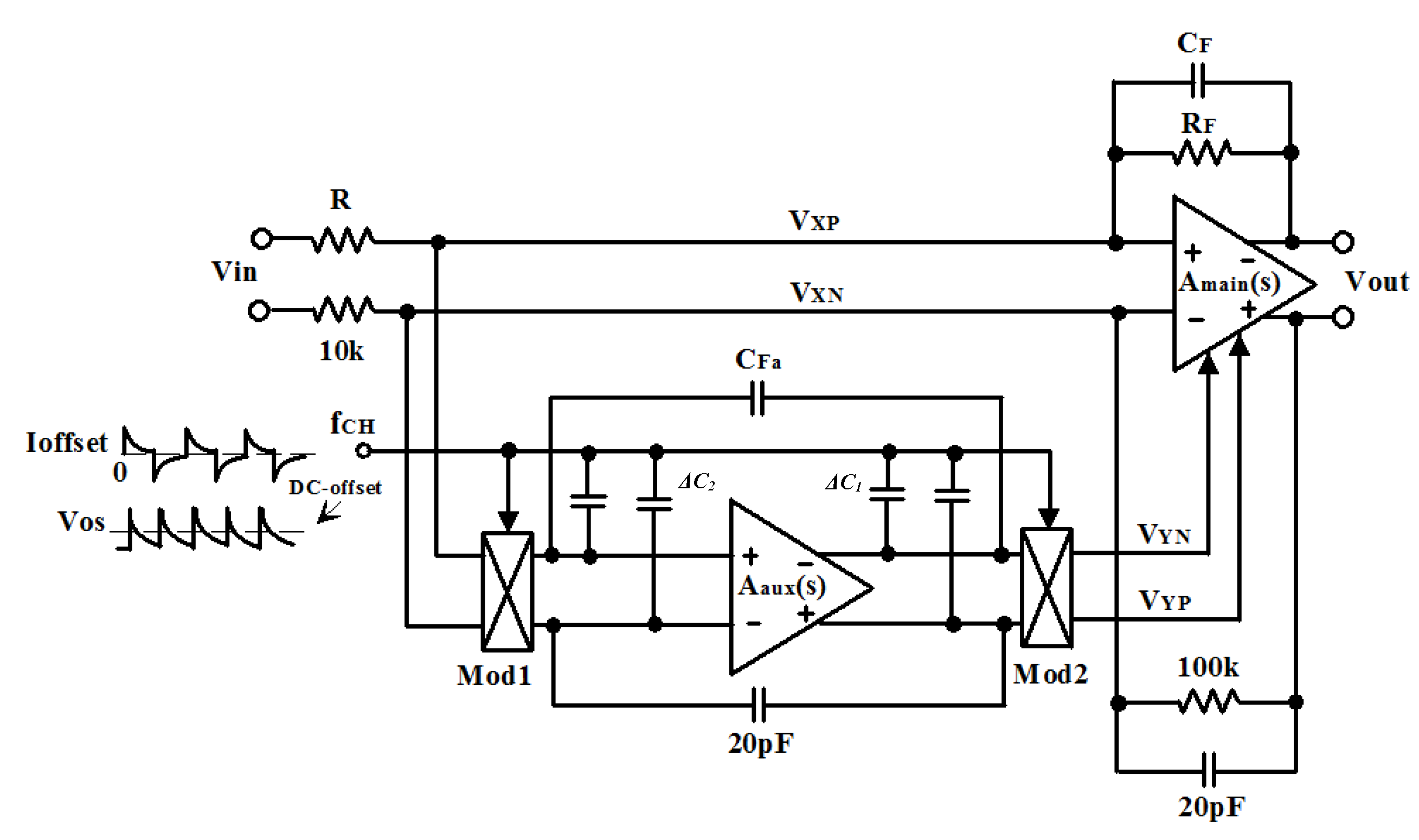
To reduce the input-equivalent noise of the preamplifier, we propose to use the well-known CHS technique. The CHS preamplifier circuit is shown in
Figure 1 [
27]. It is composed by the main amplifier,
Amain(
s), and by the auxiliary amplifier,
Aaux(
s). The non-idealities of
Amain(
s) in low-frequency path are canceled by the
Aaux(
s). Firstly, the input signal at
Amain(
s) is measured by
Aaux(
s). Then, the virtual ground
VX = VXP − VXN is derived toward zero by
Aaux(
s). Therefore, a compensation voltage
VY = VYP − VYN is generated by the
Aaux(
s) to the
Amain(
s). The virtual ground
VX can be written as
Namely, the auxiliary amplifier allows attenuating the main amplifier noise portion as
where
is the input noise of the main amplifier with the auxiliary amplifier and
is the input noise of the main amplifier without the auxiliary amplifier.
Aaux_int(
s) represents the active RC-integrator signal transfer function (STF), which can be written as
The signal path mismatch and the demodulated current spikes generate a residual offset
Vos. Therefore, AC current spike is caused by the mismatch between the capacitances, due to clock feed-through at the chopper clocks transition moments. The first modulator Mod1 rectify this AC current. Therefore, a DC spike current appears at its input. The resulting DC spike current has an average value
Ioffset of
where Δ
C1 and Δ
C2 denote the CHS mismatch parasitic capacitance,
Vclk denotes the clock signal magnitude, and
fCH denotes the Chopping clock frequency. The chopper series impedance and the input signal source are going through by this noise current. Therefore, it depicts as an input voltage spike. The residual offset
Vos resulting from the spike average DC value can be written as
where
R denotes the equivalent input impedance. Therefore, a residual offset
Vos depicts the spike average DC value. Moreover, a spike voltage
Vos is created in the input of the Mod1. This spike voltage causes a low-frequency interference.
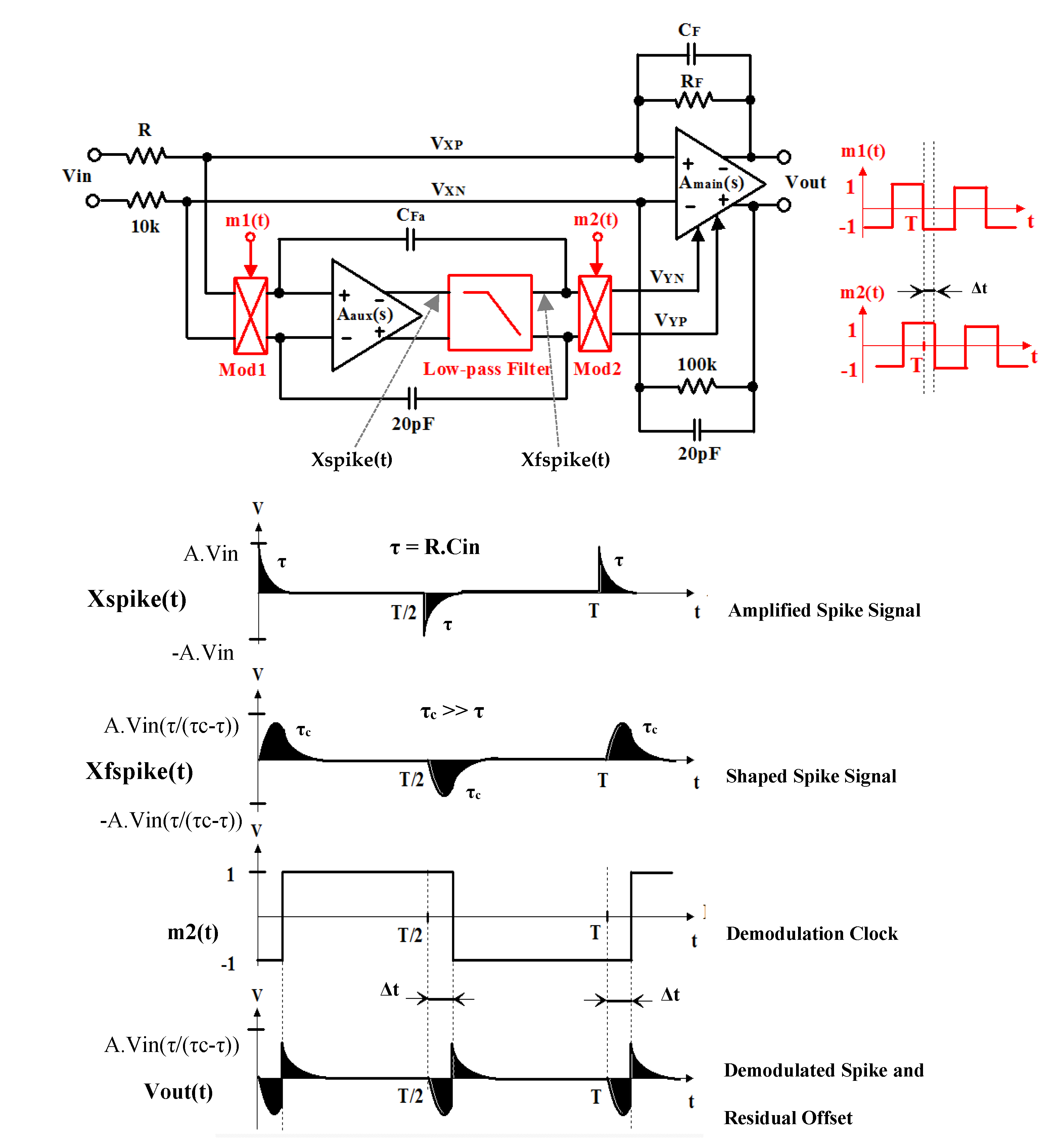
To cancel out this interference, we propose to create a proper delay Δ
t between Mod1 and Mod2. The proposed preamplifier CHS technique is shown in
Figure 2. The auxiliary amplifier is located between two modulating clock signals: m1(t) and m2(t) with period
T. Moreover, we introduce a delay ∆
t between the two clock signals m1(t) and m2(t) at the same time. Due to the introduction of the delay ∆
t, this technique causes a chopping of the spike signal itself. Therefore, the DC content of the output signal
Vout(t) is minimized. The residual output DC offset is completely cancelled if an optimum delay value ∆
topt exists, which can be written as
where
τ = R × C
in with
R, and C
in denotes respectively the input resistance and the amplifier’s input capacitance.
The major weakness of this technique is the τ itself, which not only depends on the amplifier’s source resistance R, but also on its input capacitance Cin. The input preamplifier’s spike signal is amplified and then multiplied with m2(t). The resulting output signal VY then contains, apart from higher order harmonics of the chopping frequency, a DC part or residual offset, which is due to chopping artifacts. To solve this problem, shaping of the spike can be introduced by the addition of a first order low-pass filter with time constant τc after Aaux(s). We must have T >> τc >> τ with T is the period of the square wave signal m1(t). The shape of the time response of the filtered spike is primarily determined by τc. Since the output offset is still linearly dependent on τ, the optimization of ∆topt has been done in such a way that offset reduction is most effective for a worst-case preamplifier resistance. For our specific implementation ∆topt/τc = 0.8 has been chosen. The low-pass filter has a cut-off frequency of 300 kHz. The nominal chopping frequency fCH is 120 kHz.
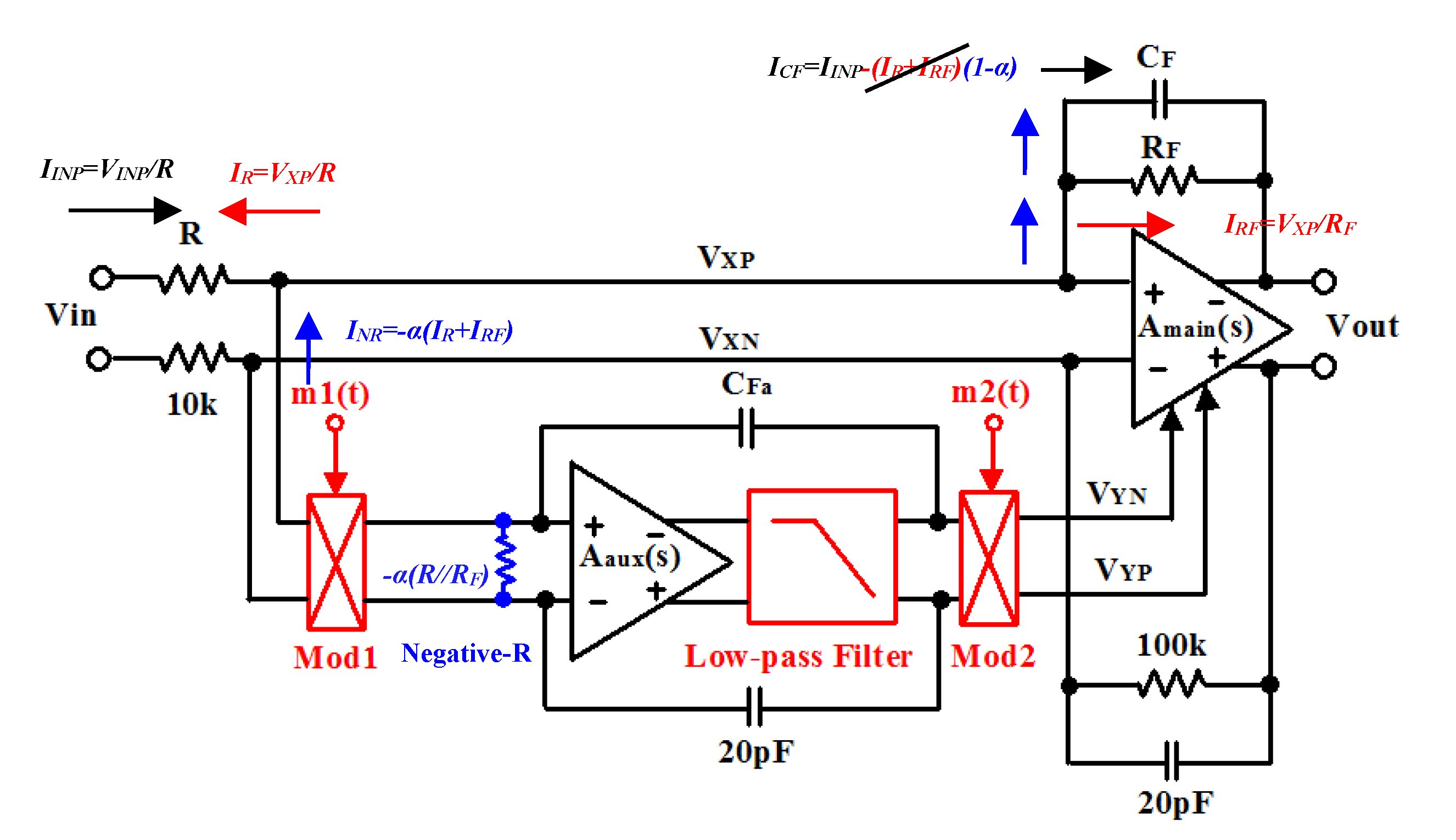
3. Analysis of the Chopper Negative-R Stabilization Preamplifier
The delay-time chopper stabilization removes only the 1/
f noise of the preamplifier. However, the chopper does not affect the
Aaux(
s) thermal noise, and the overall noise level of the preamplifier is not reduced. Likewise, a large bandwidth of
Aaux(
s) is required in order to keep its high gain at
fCH. To reduce both the 1/
f noise and the thermal noise, we propose to use the chopper negative-R stabilization circuit as shown in
Figure 3. This proposed technique allows removing the preamplifier non-ideality at
VX. It will compensate for the error current I
R and I
RF generated by
R and
RF, respectively at
VX. Therefore, we choose the negative-R value in order to matching the value of the parallel resistors
R//
RF. As a result, the chopper negative-R stabilization technique allows mitigating the
VX error. In the first case, the preamplifier noise is analyzed without the negative-R circuit. The overall main and auxiliary opamps noise transfer function (NTF) can be written as
where
denotes the input-referred noise of preamplifier, and
denotes the noise of opamps. The
noise are calculated at the preamplifier input node. In the second case, the preamplifier noise is analyzed with the chopper negative-R circuit. The overall main and auxiliary opamps NTF becomes
where the very important coefficient
α denotes the negative-R matching coefficient of the parallel resistors
R//
RF. If
α becomes closer to 2, ideal compensation for
α = 1, the noise opamps decreases.
However, the negative-R circuit adds an amount of noise of
, with
in this case. As a result, the proposed negative-R preamplifier has an input-referred noise of
where
|H(s)|2 denotes the NTF of the negative-R opamps of Equation (8). Therefore, the chopper negative-R circuit allows attenuating the opamps mismatch and offset.
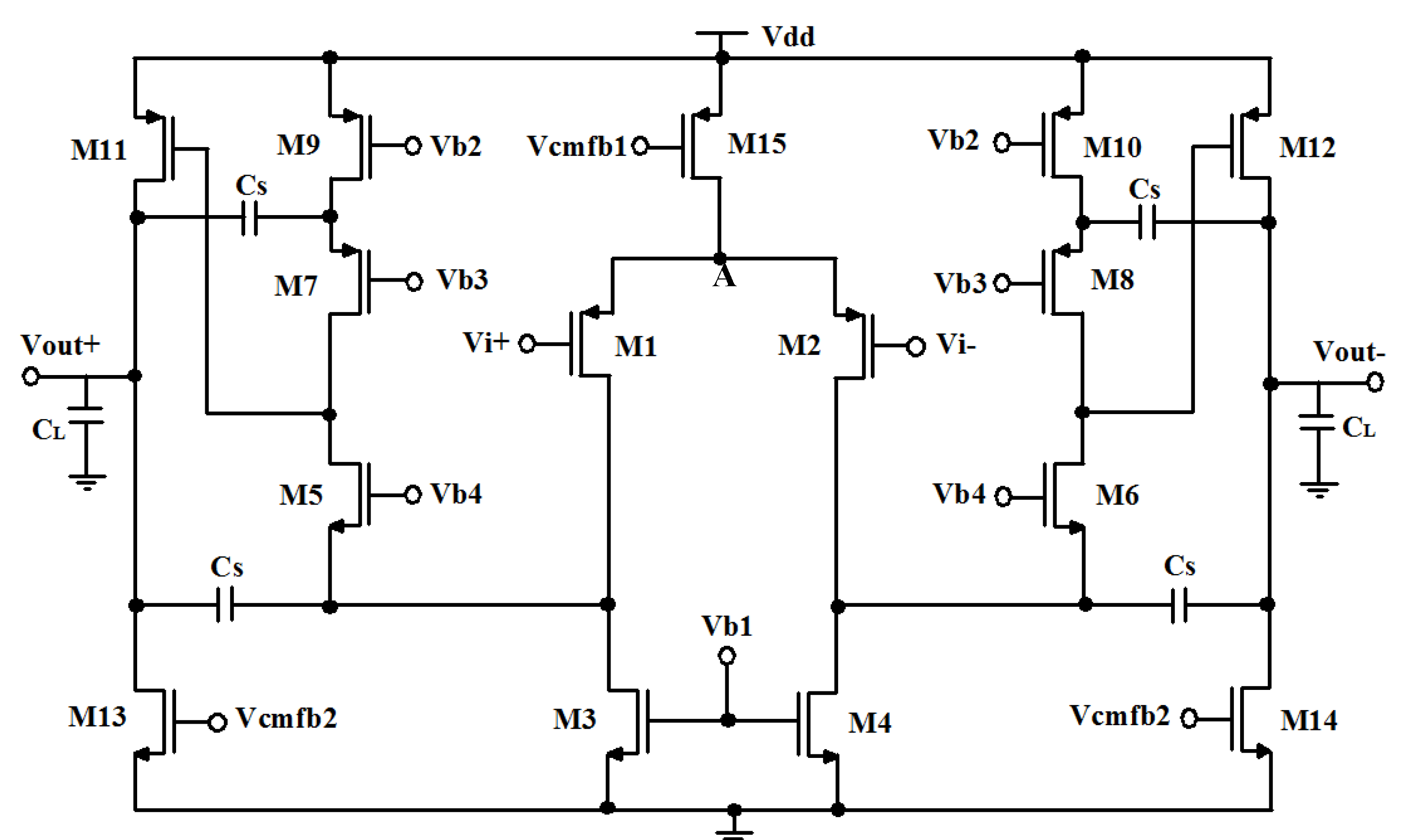
4. CMOS Amplifier Implementation
If the amplifier is designed with a single-stage topology under low-voltage operation, then its output swing and its gain are limited. Usually, an amplifier with a two-stage topology, as shown in
Figure 4, is used to increase the gain and the output swing. The first stage of the amplifier contributes to the total gain while the second stage contributes to enable a large output swing. The compensation capacitor (
CS) allows stabilizing the two-stage amplifier. In order to improve the frequency response, a resistor is connected in series with the capacitor
CS. Therefore, the amplifier receives a left half plane zero [
28].
A desired gain-bandwidth (GBW) and a load capacitance (
CL) are considered to evaluate the amplifier power consumption. If all amplifier transistors have the same overdrive voltage
, and if the output non-dominant pole is at least three times of the GBW, then the current consumption
Itwo-stage of the two-stage operational transconductance amplifier (OTA) can be written as [
29,
30].
From Equation (10), it is clear that the maximum of the current is used to drive the compensation capacitors.
Figure 4 shows the schematic of two-stage amplifier. The first stage is a differential OTA providing high gain, while the second stage is configured as a simple common-source stage to give maximum output swing. In contrast to cascode opamps, this topology isolates the gain and output swing requirements [
29,
30]. The DC-gain Ad and GBW expressions of the amplifier is given as
where
gm1 and
gm3 denote the transconductance of transistor M1 and M3,
r01,
r02,
r03, and
r011 denote the output resistance of transistors M1, M2, M3, and M11, respectively. Assuming all the transistors have the same overdrive voltage, the transconductance
gm of M1 and M3 can be written as
where
ID denotes the drain current,
VT denotes the threshold voltage, and
VGS denotes the gate-source voltage of the MOSFET. Further, assuming all branches have the same current and ignoring parasitic capacitance at node
A, Equation (12) can be modified as
where
λ denotes the channel-length modulation parameter of the MOSFET. Combining Equations (13)–(15), the total current of the two-stage OTA is then
Since the parasitic capacitor at node A is negligible, for more power saving, the frequency compensation is performed by the load capacitance, and no miller compensation is used. The maximum output swing that this amplifier can achieve is . To achieve a higher signal swing, the overdrive voltage of transistors M4 and M5 are minimized in this design. The two-stage OTA has an open-loop gain of 65-dB, a phase margin of 62°, and a GBW of 16-MHz, with a power consumption of only 72-μW.
The noise sources of the CMOS operational amplifier originate from flicker noise and thermal noise components. The flicker noise component is usually larger than the thermal noise component for frequencies from 1 Hz to 20 kHz for a typical bias conditions and device geometries. The total noise current of a MOSFET is given as [
30]
Neglecting the thermal noise contribution, the total noise current can be approximated as:
with:
where
KF is the flicker noise coefficient,
gm is the transconductance parameter of the MOSFET device,
COX is the gate-oxide capacitance per unit area,
W is the channel width,
L is the channel length,
f is the frequency,
m represents the effective mobility,
ID is the drain current, and Δ
f is the bandwidth. Thus, the equivalent input-referred voltage noise can be written as:
Noise analysis of the two-stage operational amplifier of
Figure 4 yields
where
denotes the thermal noise of transistor M1, and
denotes the thermal noise of transistor M3. Substituting Equations (19) and (20) into Equation (21), we have
where the symbols have their usual meanings, and the subscript n represents n-channel device, and subscript p represents p-channel device. It is apparent from Equation (22) that there exists a minimum as
L1 varies. For very low values of
L1, the first term is dominant, whereas for large
L1 values, the second term is dominant. Although the low-noise design practice adapts long channel length
L3 for active load and short channel length
L1 for good phase margin.
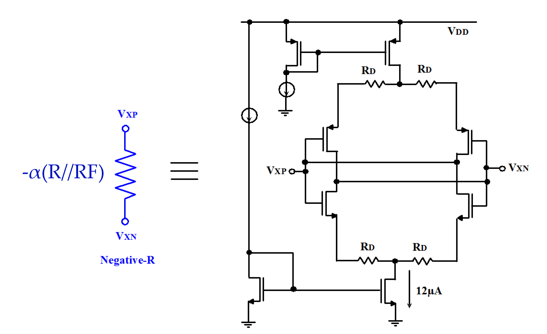
The transistor-level circuit of the negative-R is shown in
Figure 5. It is implemented in a topology of MOSFET source-degeneration. It consumes only 12-μW. In this topology, the degeneration resistor and the current source allows enhancing the accuracy of matching the circuit within 10%. Moreover, a stable
gm of the negative-R is maintained over the temperature and power supply variations [
26].
5. Measurement Results
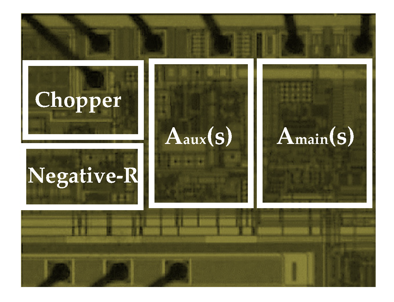
Prototypes of the low-noise preamplifier are fabricated and experimentally characterized. The die microphotograph of the preamplifier is shown in
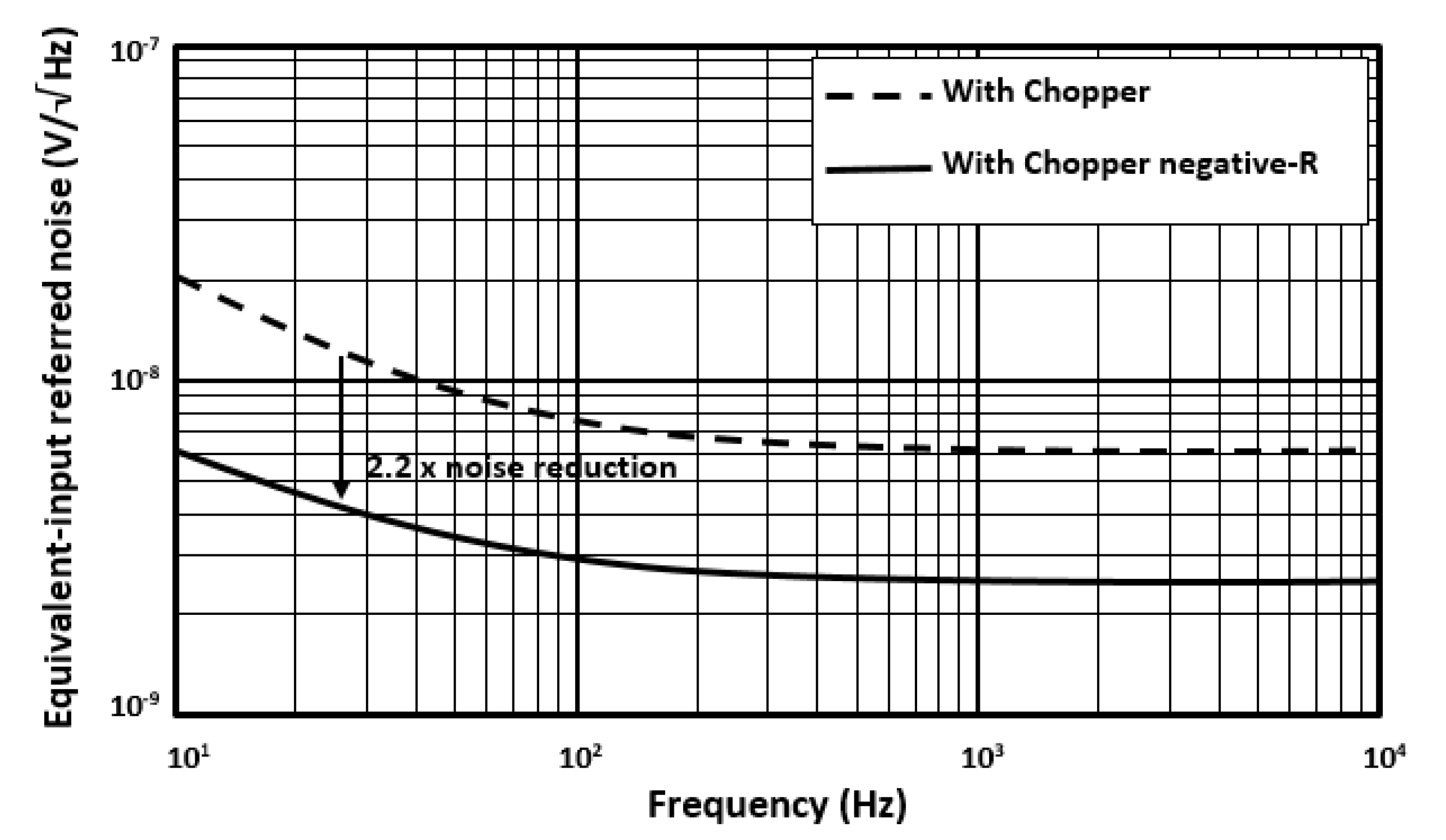
Figure 6. The measurement result of the preamplifier input-referred noise with CHS circuit and with chopper negative-R circuit is shown in
Figure 7. The preamplifier has a bandwidth of 20 kHz. From measurement result, if the preamplifier is with CHS circuit, then its input-referred noise is 11 nV/√Hz. If the preamplifier is with chopper negative-R circuit, then its input-referred noise is almost limited by the R, R
F, and negative-R thermal noise and it is attenuated to 5 nV/√Hz. Moreover, it is clear from measurement result that the chopper negative-R circuit allows to mitigate the opamps 1/
f noise and thermal noise. As a result, the proposed chopper negative-R stabilization preamplifier allows a noise reduction of 2.2 times, compared to the conventional preamplifier. The curves in
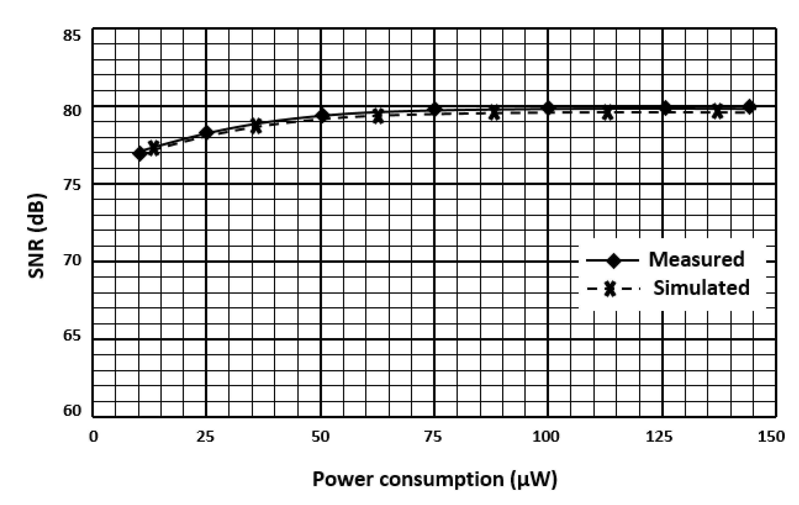
Figure 8 show the SNR of the preamplifier as a function of the power consumption. Simulation results have been added for comparison. It appears that the evolution of the experimentally measured SNR is consistent with that obtained with the simulation results. The maximum measured SNR is 80 dB. This value is nearly the same as the simulation result. It is obtained for a current of 132 μA. It corresponds to a power consumption of 159 µW.
The measurement results of the proposed low-noise preamplifier and the comparison with other amplifiers is reported in
Table 1. A fundamental parameter is used to evaluate the overall power efficiency of the preamplifier. This parameter is the noise efficiency factor parameter (NEF), which can be written as [
31]
where
Itotal is the total current consumption,
Vrms is the root-mean square (RMS) input-referred noise,
Uth is the thermal voltage, and
BW is the bandwidth of the preamplifier. From Equation (23), it is clear that the NEF parameter includes almost every performance shown in
Table 1, namely the equivalent-input referred noise, the power consumption, the bandwidth and indirectly the power-supply rejection ratio (PSRR), and the common-mode rejection ratio (CMRR). In [
32,
33], the preamplifier has a high CMRR and high PSRR. However, it has also a high equivalent-input referred noise at list of about 18 nV/√Hz. In [
22,
23], the measured preamplifier has a low CMRR and low PSRR. Moreover, it has a worse equivalent-input referred noise at least 47 nV/√Hz. Therefore, this noise level affects drastically the preamplifier and degrades its performances. As a result, all compared preamplifiers have an equivalent-input referred noise greater than 18 nV/√Hz. On the other hand, our measured preamplifier has a high CMRR and high PSRR. Moreover, it has the lowest equivalent-input referred noise of only 5 nV/√vHz. As a result, for the same performances, our preamplifier has a good tradeoff between the supply voltage, the PSRR, and the CMRR. Our proposed circuit achieves a NEF of 1.9, a PSRR of 110 dB and a CMRR of 121 dB. Therefore, it proves a competitive performance compared to the state-of-the art.


