A Carbon Nanotube–Metal Oxide Hybrid Material for Visible-Blind Flexible UV-Sensor


Abstract
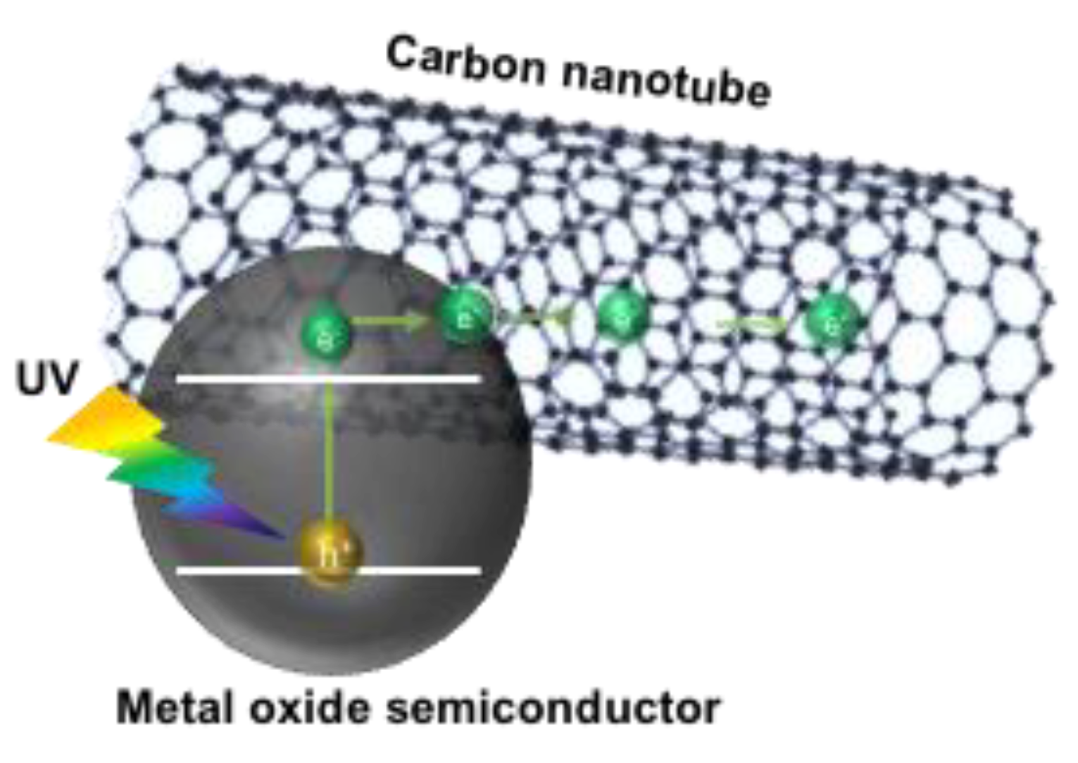
1. Introduction
2. Materials and Methods
2.1. Chemicals
2.2. ZnO Nanoparticle Synthesis
2.3. Preparation of OH-MWCNT/ZnO Nanocomposite
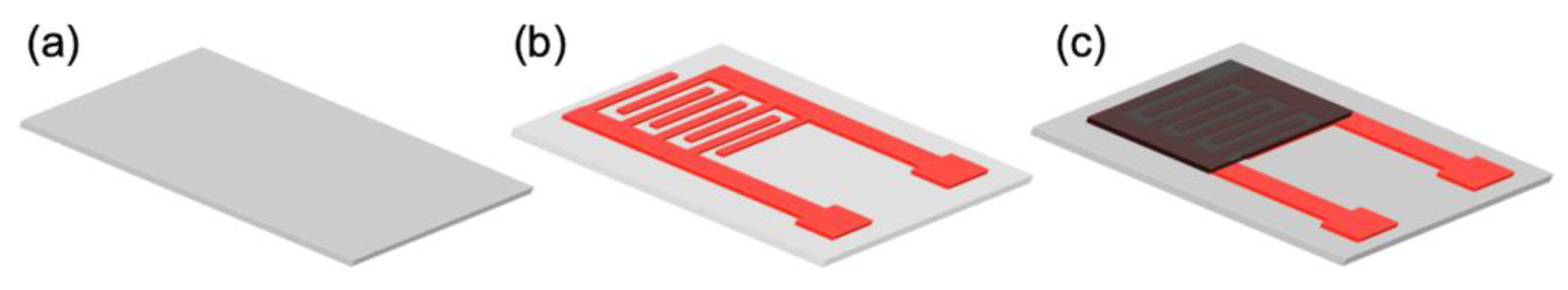
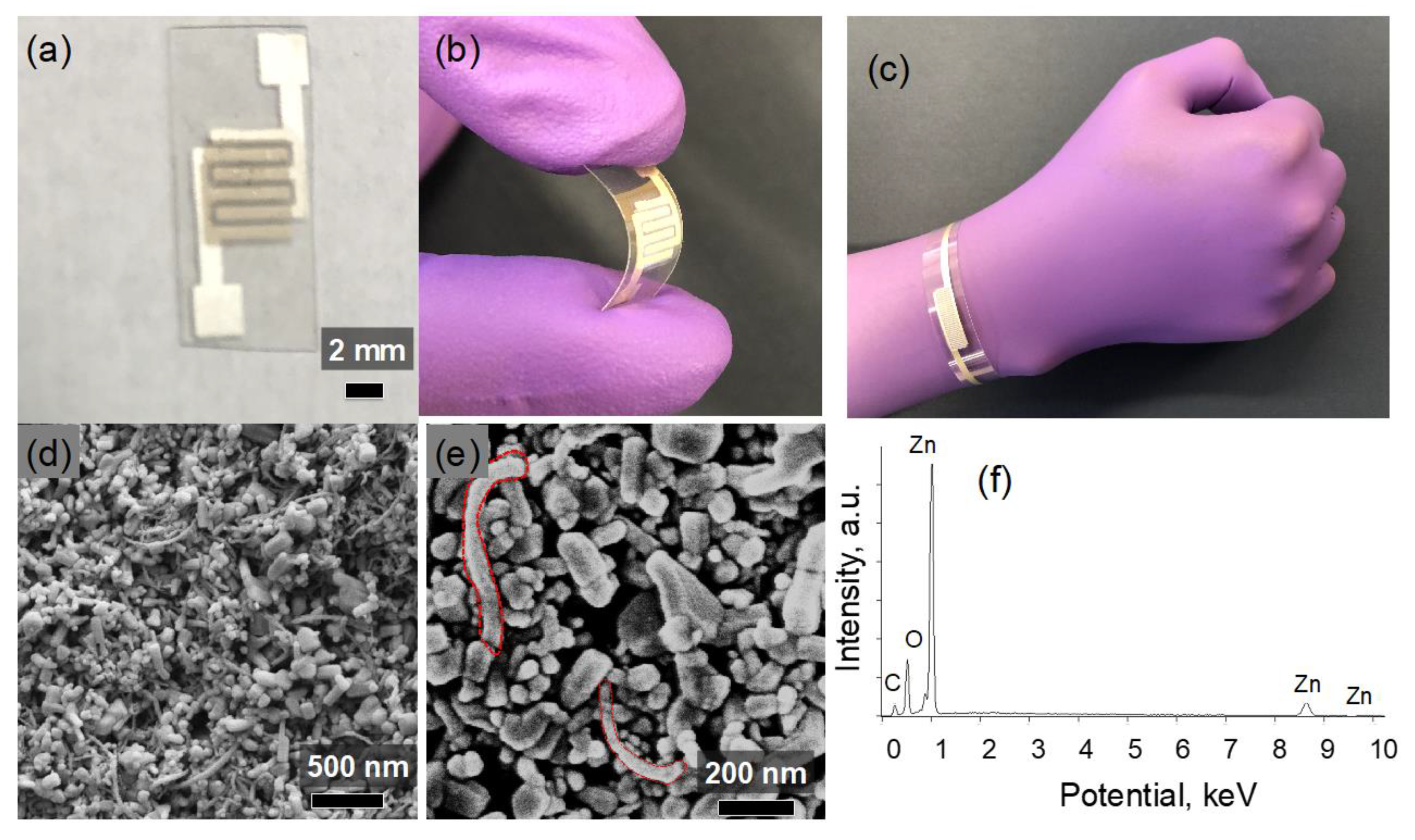
2.4. Device Fabrication
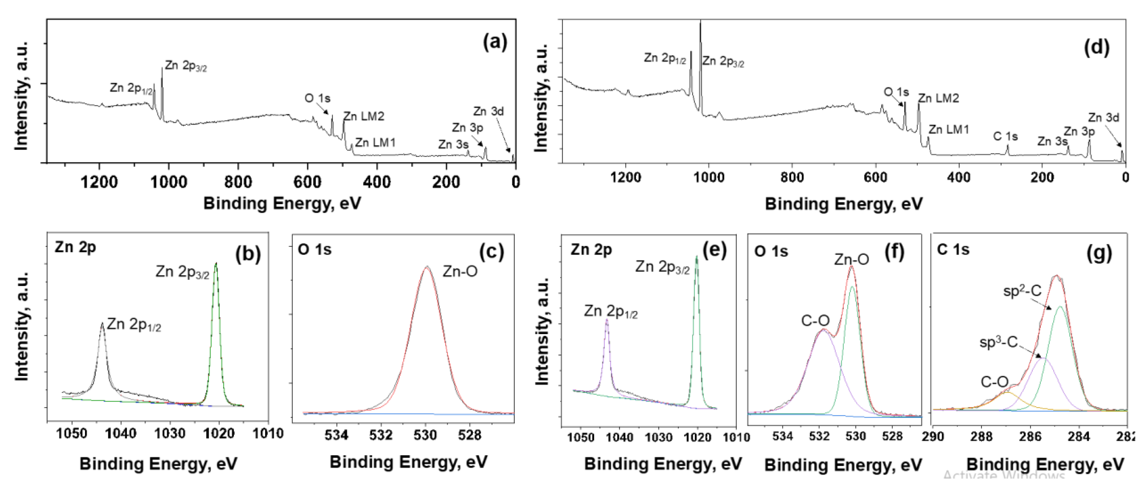
2.5. Materials Characterization
3. Results and Discussion
3.1. Morphology Analysis
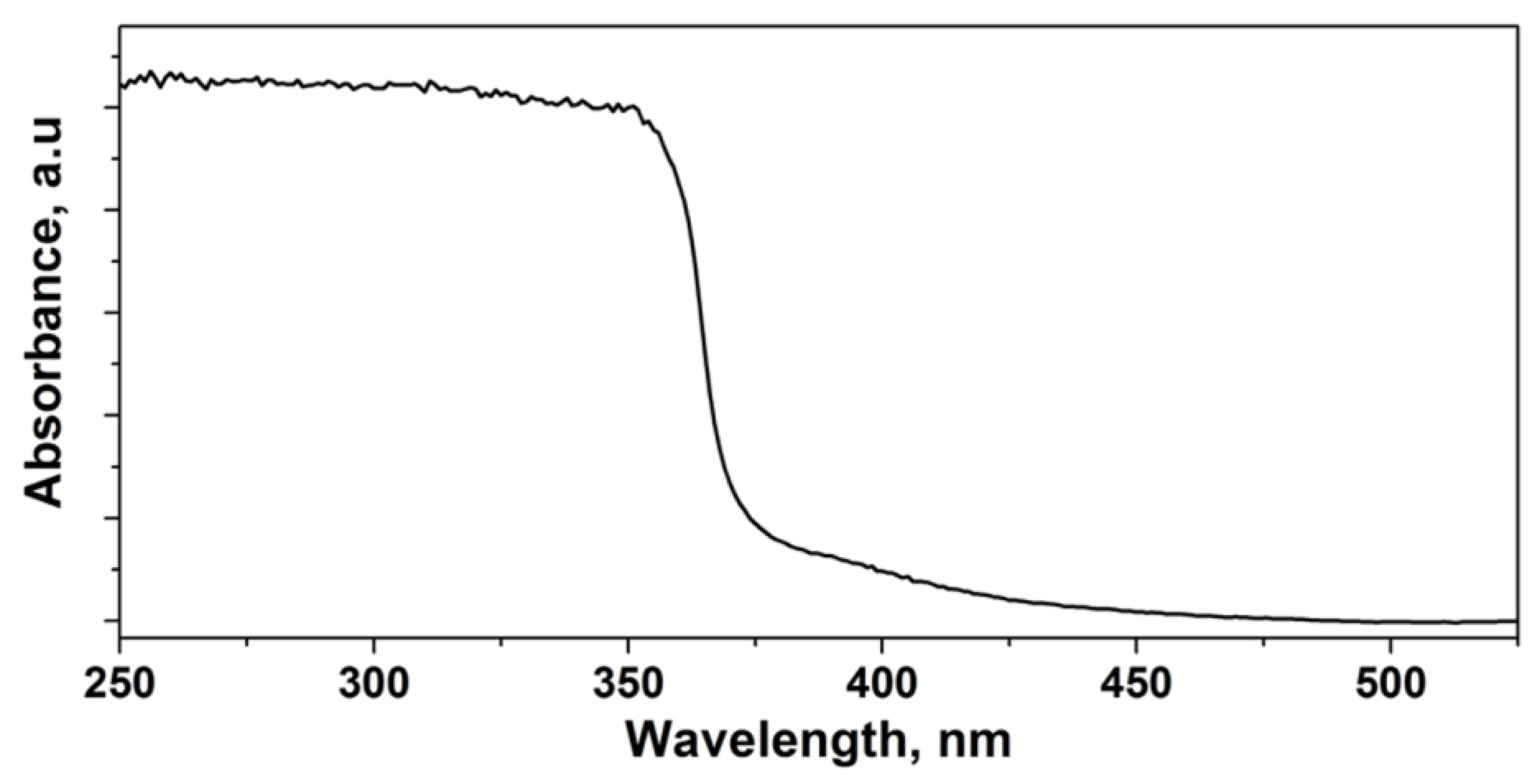
3.2. Optical Absorbance of the Films
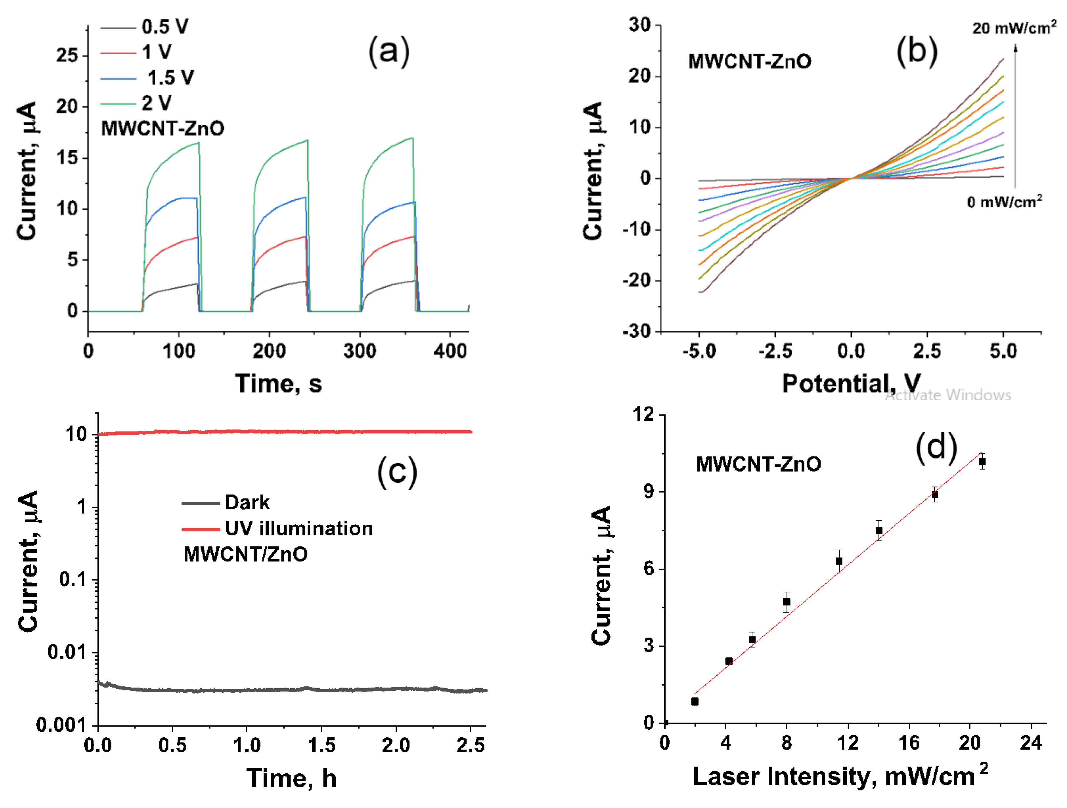
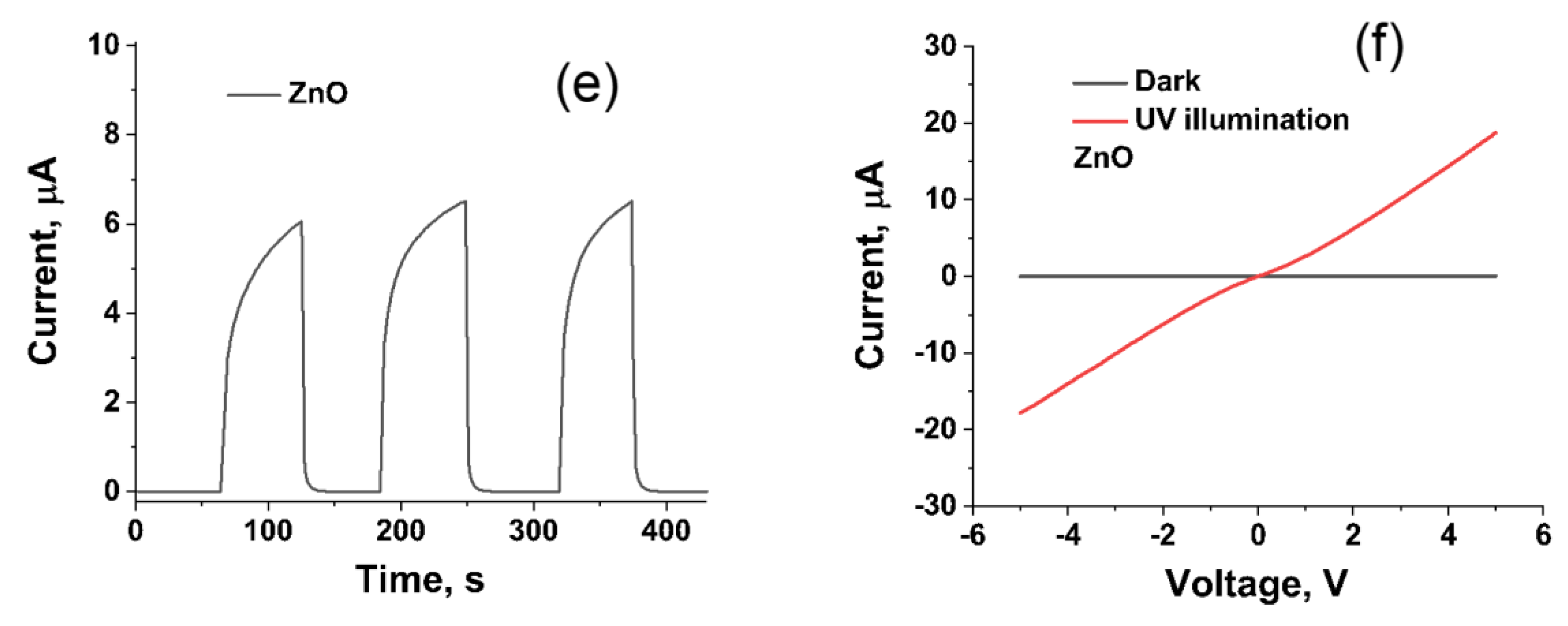
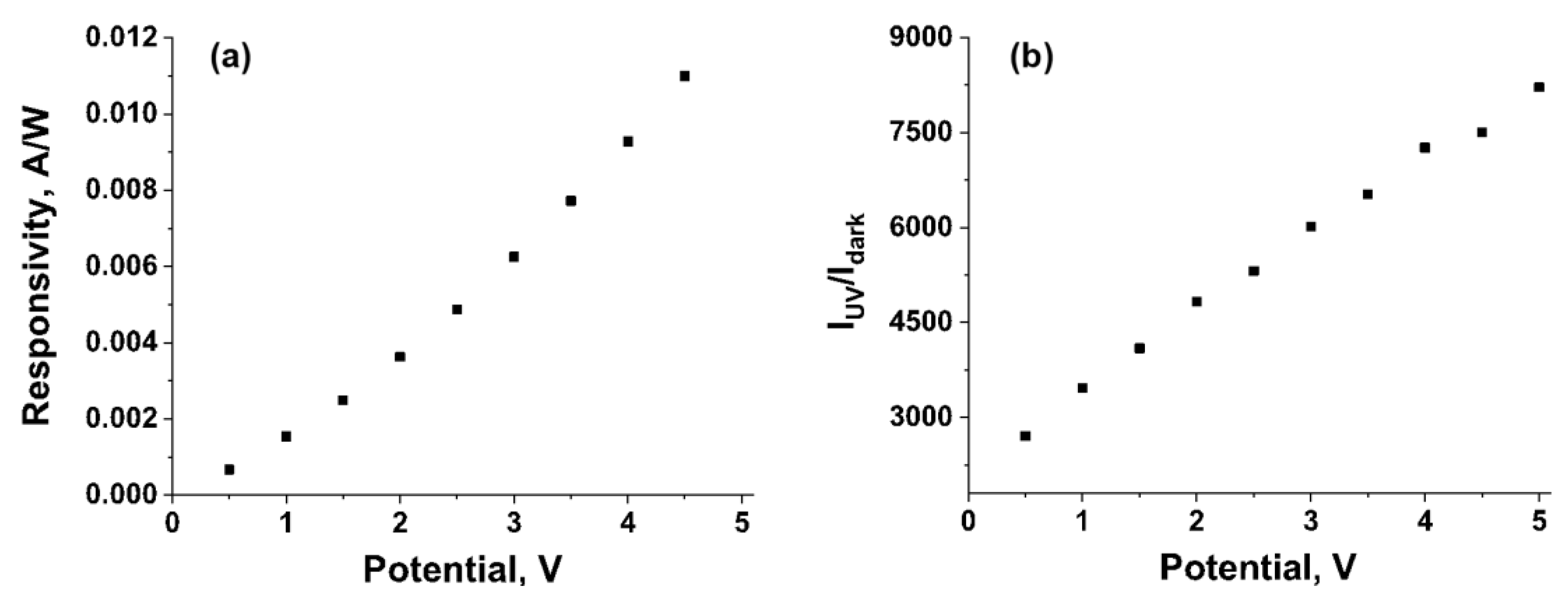
3.3. Sensor Response
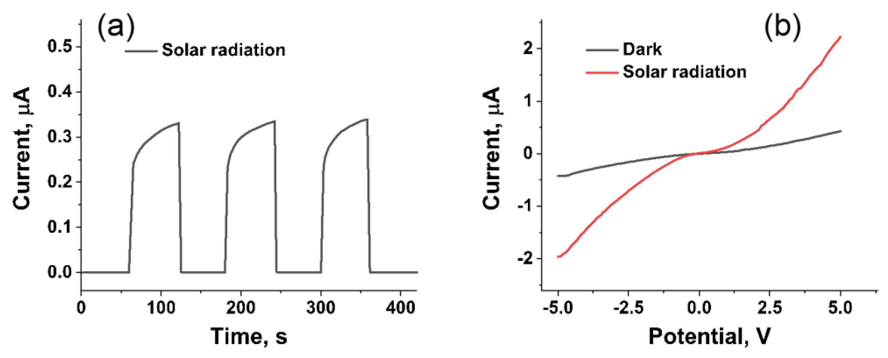
3.4. Response of Device under Solar Radiation
4. Conclusions
Author Contributions
Funding
Conflicts of Interest
References
- Moan, J. Ozone holes and biological consequences. J. Photochem. Photobiol. B Biol. 1991, 9, 244–247. [Google Scholar] [CrossRef]
- Henriksen, T.; Dahlback, A.; Larsen, S.H.; Moan, J. Ultraviolet-radiation and skin cancer. Effect of an ozone layer depletion. Photochem. Photobiol. 1990, 51, 579–582. [Google Scholar] [CrossRef] [PubMed]
- Brash, D.E.; Rudolph, J.A.; Simon, J.A.; Lin, A.; McKenna, G.J.; Baden, H.P.; Halperin, A.J.; Ponten, J. A role for sunlight in skin cancer: UV-induced p53 mutations in squamous cell carcinoma. Proc. Natl. Acad. Sci. USA 1991, 88, 10124–10128. [Google Scholar] [CrossRef] [PubMed]
- Wang, X.; Cho, H.J. p-CuO nanowire/n-ZnO nanosheet heterojunction-based near-uv sensor fabricated by electroplating and thermal oxidation process. Mater. Lett. 2018, 223, 170–173. [Google Scholar] [CrossRef]
- Chen, Y.-C.; Lu, Y.-J.; Lin, C.-N.; Tian, Y.-Z.; Gao, C.-J.; Dong, L.; Shan, C.-X. Self-powered diamond/β-Ga2O3 photodetectors for solar-blind imaging. J. Mater. Chem. C 2018, 6, 5727–5732. [Google Scholar] [CrossRef]
- Yang, D.; Ma, D. Development of organic semiconductor photodetectors: From mechanism to applications. Adv. Opt. Mater. 2019, 7, 1800522. [Google Scholar] [CrossRef]
- Pathak, P.; Podzorski, M.; Bahnemann, D.; Subramanian, V.R. One-Pot Fabrication of High Coverage PbS Quantum Dot Nanocrystal-Sensitized Titania Nanotubes for Photoelectrochemical Processes. J. Phys. Chem. C 2018, 122, 13659–13668. [Google Scholar] [CrossRef]
- Bamshad, A.; Cho, H.J. Digital Microfabrication on Paper and Cloth for Heavy Metal Detection and Remediation. In Proceedings of the 2019 20th International Conference on Solid-State Sensors, Actuators and Microsystems & Eurosensors XXXIII (TRANSDUCERS & EUROSENSORS XXXIII), Berlin, Germany, 23–27 June 2019; pp. 685–688. [Google Scholar]
- Pathak, P.; Gupta, S.; Grosulak, K.; Imahori, H.; Subramanian, V. Nature-inspired tree-like TiO2 architecture: A 3D platform for the assembly of CdS and reduced graphene oxide for photoelectrochemical processes. J. Phys. Chem. C 2015, 119, 7543–7553. [Google Scholar] [CrossRef]
- Sun, Y.-F.; Liu, S.-B.; Meng, F.-L.; Liu, J.-Y.; Jin, Z.; Kong, L.-T.; Liu, J.-H. Metal oxide nanostructures and their gas sensing properties: A review. Sensors 2012, 12, 2610–2631. [Google Scholar] [CrossRef]
- Zhai, T.; Fang, X.; Liao, M.; Xu, X.; Zeng, H.; Yoshio, B.; Golberg, D. A comprehensive review of one-dimensional metal-oxide nanostructure photodetectors. Sensors 2009, 9, 6504–6529. [Google Scholar] [CrossRef]
- Xu, Q.; Cheng, L.; Meng, L.; Wang, Z.; Bai, S.; Tian, X.; Jia, X.; Qin, Y. Flexible Self-Powered ZnO Film UV Sensor with a High Response. ACS Appl. Mater. Interfaces 2019, 11, 26127–26133. [Google Scholar] [CrossRef] [PubMed]
- Pathak, P.; Israel, L.H.; Pereira, E.J.M.; Subramanian, V.R. Effects of carbon allotrope interface on the photoactivity of rutile one-dimensional (1D) TiO2 coated with anatase TiO2 and sensitized with CdS nanocrystals. ACS Appl. Mater. Interfaces 2016, 8, 13400–13409. [Google Scholar] [CrossRef] [PubMed]
- Chen, T.; Wang, S.; Yang, Z.; Feng, Q.; Sun, X.; Li, L.; Wang, Z.S.; Peng, H. Flexible, light-weight, ultrastrong, and semiconductive carbon nanotube fibers for a highly efficient solar cell. Angew. Chem. Int. Ed. 2011, 50, 1815–1819. [Google Scholar] [CrossRef] [PubMed]
- Hirsch, A. The era of carbon allotropes. Nat. Mater. 2010, 9, 868–871. [Google Scholar] [CrossRef] [PubMed]
- Kongkanand, A.; Martínez Domínguez, R.; Kamat, P.V. Single wall carbon nanotube scaffolds for photoelectrochemical solar cells. Capture and transport of photogenerated electrons. Nano Lett. 2007, 7, 676–680. [Google Scholar] [CrossRef]
- Wang, R.-C.; Hsu, C.-C.; Chen, S.-J. The evolution of well-aligned amorphous carbon nanotubes and porous ZnO/C core–shell nanorod arrays for photosensor applications. Nanotechnology 2010, 22, 035704. [Google Scholar] [CrossRef]
- Boruah, B.D.; Misra, A. Conjugated assembly of colloidal zinc oxide quantum dots and multiwalled carbon nanotubes for an excellent photosensitive ultraviolet photodetector. Nanotechnology 2016, 27, 355204. [Google Scholar] [CrossRef]
- Safa, S. Enhanced UV-detection properties of carbon nanotube impregnated ZnO nanourchins. Opt. Int. J. Light Electron Opt. 2015, 126, 2194–2198. [Google Scholar] [CrossRef]
- Lupan, O.; Schütt, F.; Postica, V.; Smazna, D.; Mishra, Y.K.; Adelung, R. Sensing performances of pure and hybridized carbon nanotubes-ZnO nanowire networks: A detailed study. Sci. Rep. 2017, 7, 1–12. [Google Scholar] [CrossRef]
- Yi, P.; Chen, K.L. Influence of surface oxidation on the aggregation and deposition kinetics of multiwalled carbon nanotubes in monovalent and divalent electrolytes. Langmuir 2011, 27, 3588–3599. [Google Scholar] [CrossRef]
- Al Abdullah, K.; Awad, S.; Zaraket, J.; Salame, C. Synthesis of ZnO nanopowders by using sol-gel and studying their structural and electrical properties at different temperature. Energy Procedia 2017, 119, 565–570. [Google Scholar] [CrossRef]
- Ma, P.C.; Tang, B.Z.; Kim, J.-K. Effect of CNT decoration with silver nanoparticles on electrical conductivity of CNT-polymer composites. Carbon 2008, 46, 1497–1505. [Google Scholar] [CrossRef]
- Li, S.-S.; Su, Y.-K. Improvement of the performance in Cr-doped ZnO memory devices via control of oxygen defects. RSC Adv. 2019, 9, 2941–2947. [Google Scholar] [CrossRef]
- Gong, P.; Wang, J.; Sun, W.; Wu, D.; Wang, Z.; Fan, Z.; Wang, H.; Han, X.; Yang, S. Tunable photoluminescence and spectrum split from fluorinated to hydroxylated graphene. Nanoscale 2014, 6, 3316–3324. [Google Scholar] [CrossRef]
- Lee, S.W.; Yabuuchi, N.; Gallant, B.M.; Chen, S.; Kim, B.-S.; Hammond, P.T.; Shao-Horn, Y. High-power lithium batteries from functionalized carbon-nanotube electrodes. Nat. Nanotechnol. 2010, 5, 531. [Google Scholar] [CrossRef]
- Guo, L.; Zhang, H.; Zhao, D.; Li, B.; Zhang, Z.; Jiang, M.; Shen, D. High responsivity ZnO nanowires based UV detector fabricated by the dielectrophoresis method. Sens. Actuators B Chem. 2012, 166, 12–16. [Google Scholar] [CrossRef]
- El Ghissassi, F.; Baan, R.; Straif, K.; Grosse, Y.; Secretan, B.; Bouvard, V.; Benbrahim-Tallaa, L.; Guha, N.; Freeman, C.; Galichet, L. A review of human carcinogens—Part D: Radiation. Lancet Oncol. 2009, 10, 751–752. [Google Scholar] [CrossRef]


© 2020 by the authors. Licensee MDPI, Basel, Switzerland. This article is an open access article distributed under the terms and conditions of the Creative Commons Attribution (CC BY) license (http://creativecommons.org/licenses/by/4.0/).
Share and Cite
Pathak, P.; Park, S.; Cho, H.J. A Carbon Nanotube–Metal Oxide Hybrid Material for Visible-Blind Flexible UV-Sensor. Micromachines 2020, 11, 368. https://doi.org/10.3390/mi11040368
Pathak P, Park S, Cho HJ. A Carbon Nanotube–Metal Oxide Hybrid Material for Visible-Blind Flexible UV-Sensor. Micromachines. 2020; 11(4):368. https://doi.org/10.3390/mi11040368
Chicago/Turabian StylePathak, Pawan, Sanghoon Park, and Hyoung Jin Cho. 2020. "A Carbon Nanotube–Metal Oxide Hybrid Material for Visible-Blind Flexible UV-Sensor" Micromachines 11, no. 4: 368. https://doi.org/10.3390/mi11040368
APA StylePathak, P., Park, S., & Cho, H. J. (2020). A Carbon Nanotube–Metal Oxide Hybrid Material for Visible-Blind Flexible UV-Sensor. Micromachines, 11(4), 368. https://doi.org/10.3390/mi11040368