Black Metals: Optical Absorbers

 , ,
, , 
Abstract
1. Introduction
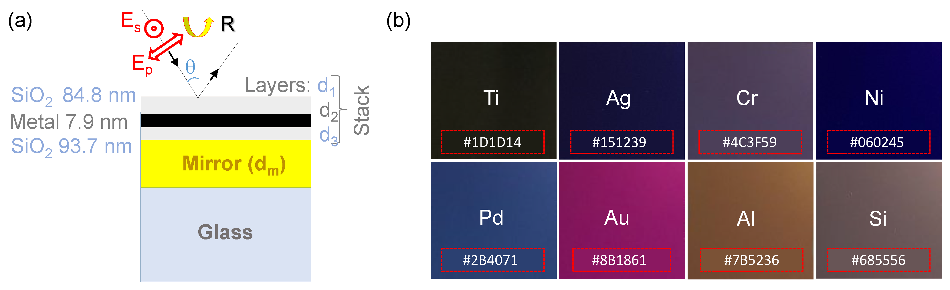
2. Theory
3. Experimental
3.1. Fabrication
3.2. Characterization
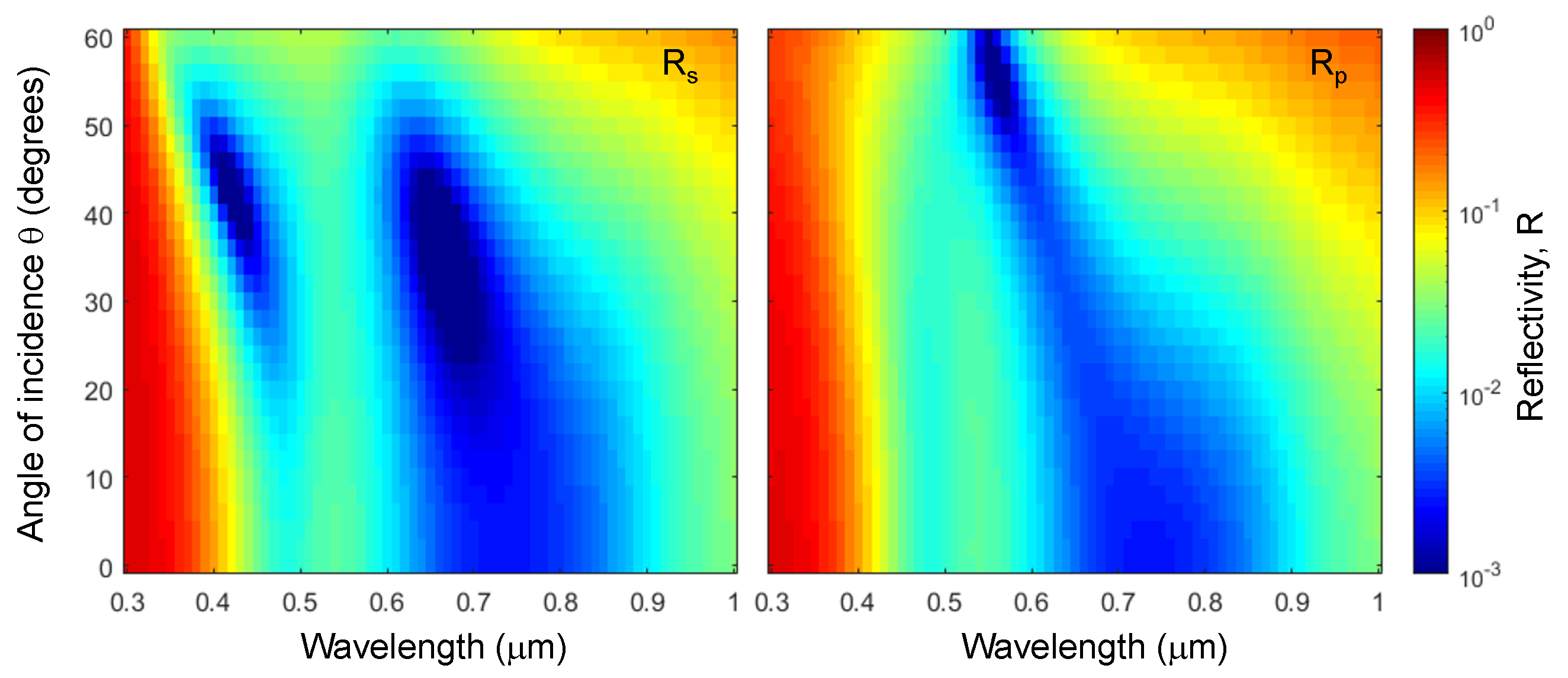
4. Results
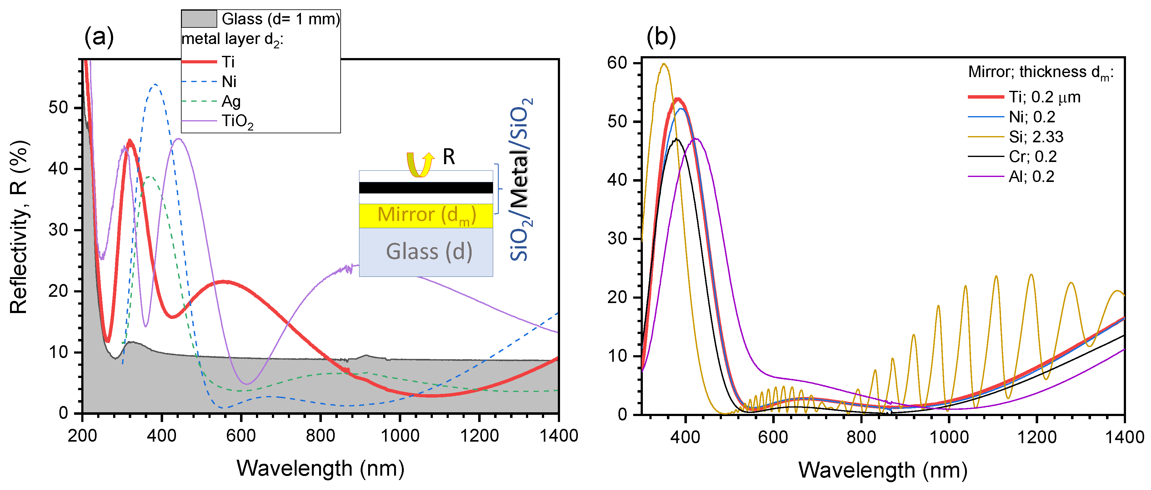
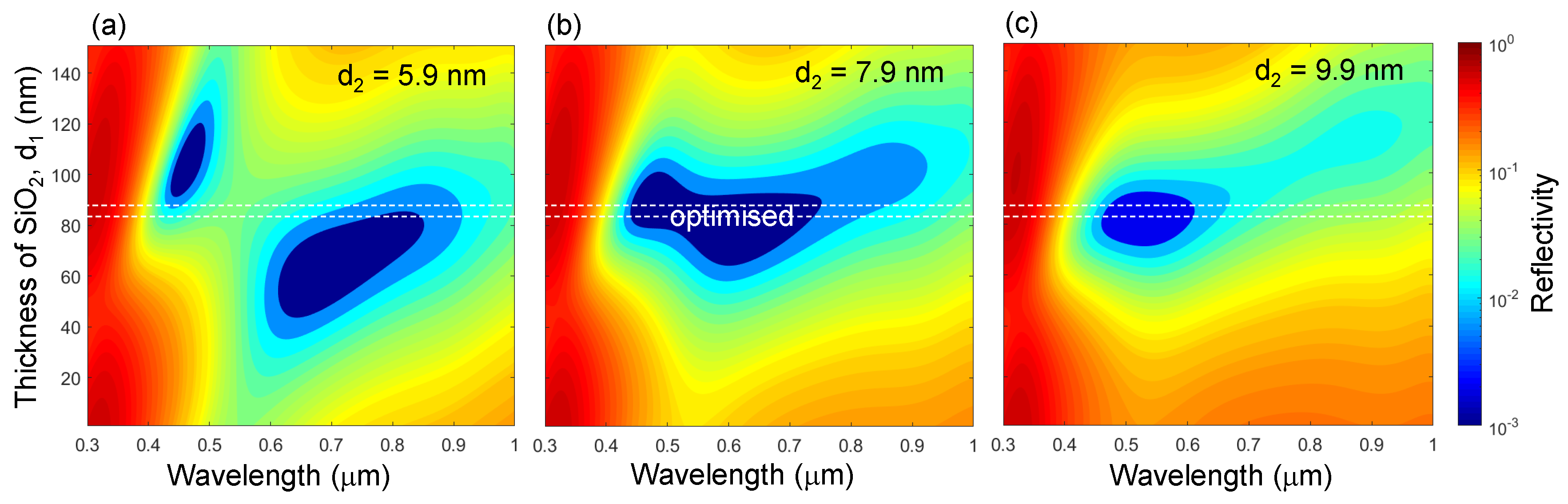
4.1. Modeling
4.2. Fabrication of Black-Metal Absorbers
5. Discussion
6. Conclusions and Outlook
Author Contributions
Funding
Acknowledgments
Conflicts of Interest
Appendix A. Parameter Study of: 1) d1 Dependence on d2,3 and 2) dm


References
- Yu, N.; Capasso, F. Flat Optics with Designer Metasurfaces. Nat. Mater. 2014, 13, 139–150. [Google Scholar] [CrossRef] [PubMed]
- Kats, M.A.; Capasso, F. Optical absorbers based on strong interference in ultra-thin films. Laser Photonics Rev. 2016, 10, 735–749. [Google Scholar] [CrossRef]
- Holloway, C.L.; Kuester, E.F.; Gordon, J.A.; O’Hara, J.; Booth, J.; Smith, D.R. An Overview of the Theory and Applications of Metasurfaces: The Two-Dimensional Equivalents of Metamaterials. IEEE Antennas Propag. Mag. 2012, 54, 10–35. [Google Scholar] [CrossRef]
- Zheludev, N.I.; Kivshar, Y.S. From metamaterials to metadevices. Nat. Mater. 2012, 11, 917–924. [Google Scholar] [CrossRef] [PubMed]
- El-Ganainy, R.; Makris, K.G.; Christodoulides, D.N.; Musslimani, Z.H. Theory of Coupled Optical PT-Symmetric Structures. Opt. Lett. 2007, 32, 2632. [Google Scholar] [CrossRef] [PubMed]
- Özdemir, K.; Rotter, S.; Nori, F.; Yang, L. Parity–Time Symmetry and Exceptional Points in Photonics. Nat. Mater. 2019, 18, 783–798. [Google Scholar] [CrossRef] [PubMed]
- Dharmavarapu, R.; Ng, S.H.; Eftekhari, F.; Juodkazis, S.; Bhattacharya, S. MetaOptics: Opensource software for designing metasurface optical element GDSII layouts. Opt. Express 2020, 28, 3505–3516. [Google Scholar] [CrossRef] [PubMed]
- Beranek, L.L.; Sleeper, H.P. The Design and Construction of Anechoic Sound Chambers. J. Acoust. Soc. Am. 1946, 18, 140–150. [Google Scholar] [CrossRef]
- Liu, N.; Mesch, M.; Weiss, T.; Hentschel, M.; Giessen, H. Infrared perfect absorber and its application as plasmonic sensor. Nano Lett. 2010, 10, 2342–2348. [Google Scholar] [CrossRef]
- Matthaei, G.L.; Young, L.; Jones, E. Microwave Filters, Impedance Inverters and Coupling Structures; McGraw-Hill Book Company, Inc.: Norwood, MA, USA, 1964; p. 1096. [Google Scholar]
- Mazilu, M.; Dholakia, K. Optical impedance of metallic nano-structures. Opt. Express 2006, 14, 7709. [Google Scholar] [CrossRef]
- Noh, H.; Chong, Y.; Stone, A.D.; Cao, H. Perfect coupling of light to surface plasmons by coherent absorption. Phys. Rev. Lett. 2012, 108, 186805. [Google Scholar] [CrossRef]
- Valentine, J.; Zhang, S.; Zentgraf, T.; Ulin-Avila, E.; Genov, D.A.; Bartal, G.; Zhang, X. Three-dimensional optical metamaterial with a negative refractive index. Nature 2008, 455, 376–379. [Google Scholar] [CrossRef]
- Stomeo, T.; Casolino, A.; Guido, F.; Qualtieri, A.; Scalora, M.; Orazio, A.D.; Vittorio, M.D.; Grande, M. 2D Dielectric Nanoimprinted PMMA Pillars on Metallo-Dielectric Films. Appl. Sci. 2019, 9, 3812. [Google Scholar] [CrossRef]
- Lawrence, F.J.; Botten, L.C.; Dossou, K.B.; Martijn de Sterke, C. Antireflection coatings for two-dimensional photonic crystals using a rigorous impedance definition. Appl. Phys. Lett. 2008, 93, 4. [Google Scholar] [CrossRef]
- Spinelli, P.; Hebbink, M.; Waele, R.D.; Black, L.; Lenzmann, F.; Polman, A. Optical Impedance Matching Using Coupled Plasmonic Nanoparticle Arrays. Nano Lett. 2011, 11, 1760–1765. [Google Scholar] [CrossRef]
- Kim, K.H.; Park, Q.H. Perfect anti-reflection from first principles. Sci. Rep. 2013, 3, 1062. [Google Scholar] [CrossRef]
- Refractive Index Database. Available online: https://refractiveindex.info/ (accessed on 26 January 2020).
- Aspnes, D.; Studna, A.A. Dielectric functions and optical parameters of Si, Ge, GaP, GaAs, GaSb, InP, InAs and InSb from 1.5 to 6.0 eV. Phys. Rev. B 1983, 27, 985–1009. [Google Scholar] [CrossRef]
- Jayawardhana, S.; Rosa, L.; Juodkazis, S.; Stoddart, P.R. Additional Enhancement of Electric Field in Surface-Enhanced Raman Scattering due to Fresnel Mechanism. Sci. Rep. 2013, 3, 2335. [Google Scholar] [CrossRef]
- Nishijima, Y.; Balčytis, A.; Naganuma, S.; Seniutinas, G.; Juodkazis, S. Tailoring Metal and Insulator Contributions in Plasmonic Perfect Absorber Metasurfaces. ACS Appl. Nano Mater. 2018, 1, 3557–3564. [Google Scholar] [CrossRef]
- Nishijima, Y.; Shimizu, S.; Kurihara, K.; Hashimoto, Y.; Takahashi, H.; Balcytis, A.; Seniutinas, G.; Okazaki, S.; Juodkazytė, J.; Iwasa, T.; et al. Optical readout of hydrogen storage in films of Au and Pd. Opt. Express 2017, 25, 24081–24092. [Google Scholar] [CrossRef]
- Grineviciute, L.; Tolenis, T.; Ryu, M.; Moein, T.; Ng, S.H.; Katkus, T.; Maksimovic, J.; Drazdys, R.; Morikawa, J.; Juodkazis, S. Releasable Micro-Waveplates. arXiv Preprint 2019, arXiv:1907.05485, 2–5. [Google Scholar]
- Nishijima, Y.; Balčytis, A.; Naganuma, S.; Seniutinas, G.; Juodkazis, S. Kirchhoff’s Metasurfaces Towards Efficient Photo-Thermal Energy Conversion. Sci. Rep. 2019, 9, 1–9. [Google Scholar] [CrossRef]
- Johnson, P.B.; Christy, R.W. Optical Constant of the Nobel Metals. Phys. Rev. B 1972, 6, 4370–4379. [Google Scholar] [CrossRef]


© 2020 by the authors. Licensee MDPI, Basel, Switzerland. This article is an open access article distributed under the terms and conditions of the Creative Commons Attribution (CC BY) license (http://creativecommons.org/licenses/by/4.0/).
Share and Cite
Lundgaard, S.; Ng, S.H.; Nishijima, Y.; Mazilu, M.; Juodkazis, S. Black Metals: Optical Absorbers. Micromachines 2020, 11, 256. https://doi.org/10.3390/mi11030256
Lundgaard S, Ng SH, Nishijima Y, Mazilu M, Juodkazis S. Black Metals: Optical Absorbers. Micromachines. 2020; 11(3):256. https://doi.org/10.3390/mi11030256
Chicago/Turabian StyleLundgaard, Stefan, Soon Hock Ng, Yoshiaki Nishijima, Michael Mazilu, and Saulius Juodkazis. 2020. "Black Metals: Optical Absorbers" Micromachines 11, no. 3: 256. https://doi.org/10.3390/mi11030256
APA StyleLundgaard, S., Ng, S. H., Nishijima, Y., Mazilu, M., & Juodkazis, S. (2020). Black Metals: Optical Absorbers. Micromachines, 11(3), 256. https://doi.org/10.3390/mi11030256