Ti Alloyed α-Ga2O3: Route towards Wide Band Gap Engineering

 , ,
, ,  and
and 
Abstract
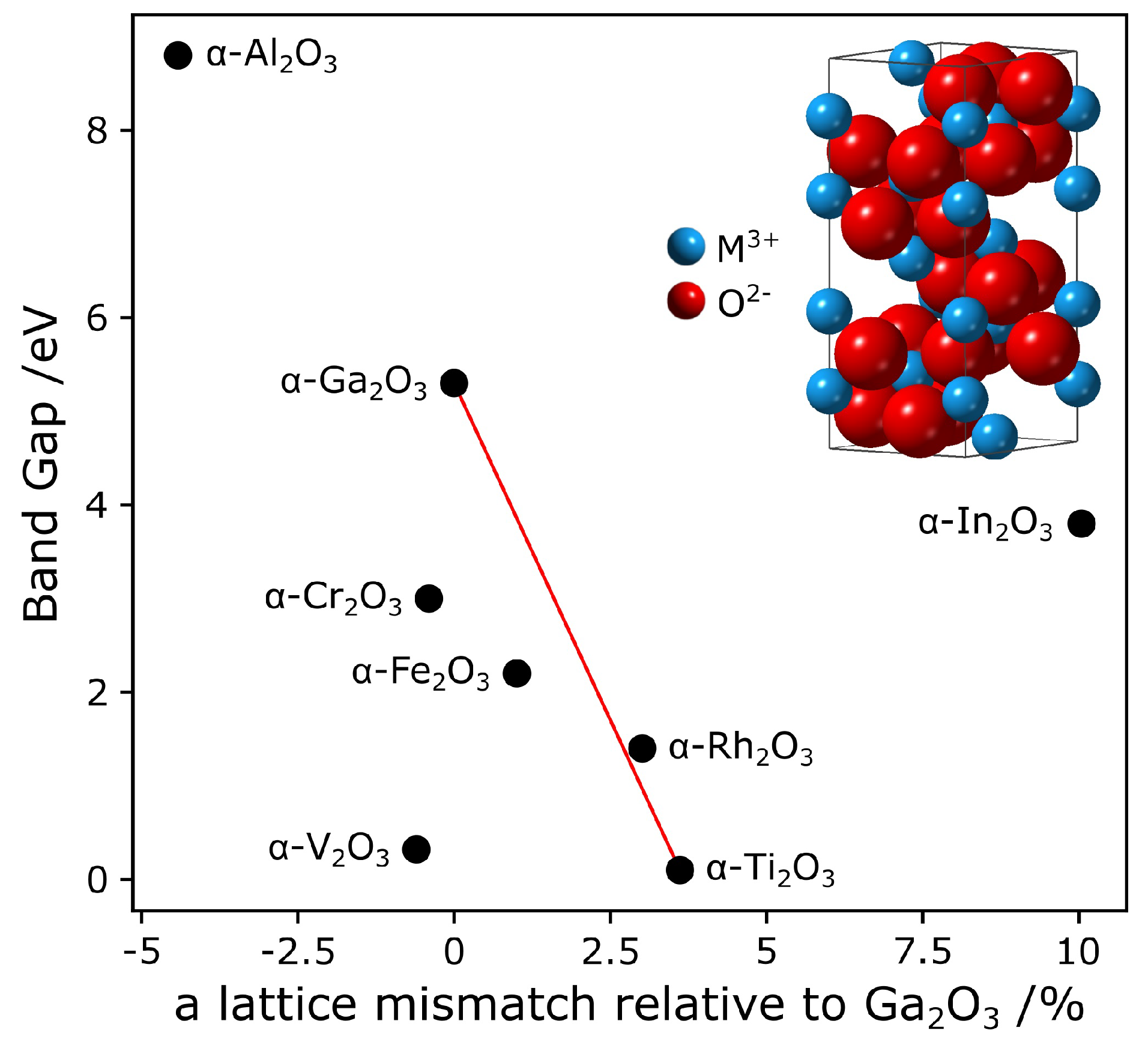
1. Introduction
2. Experimental Methods
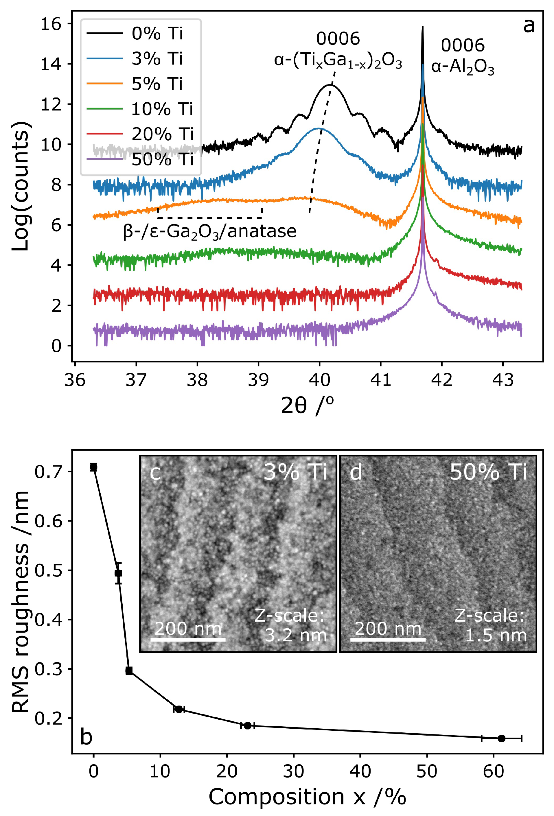
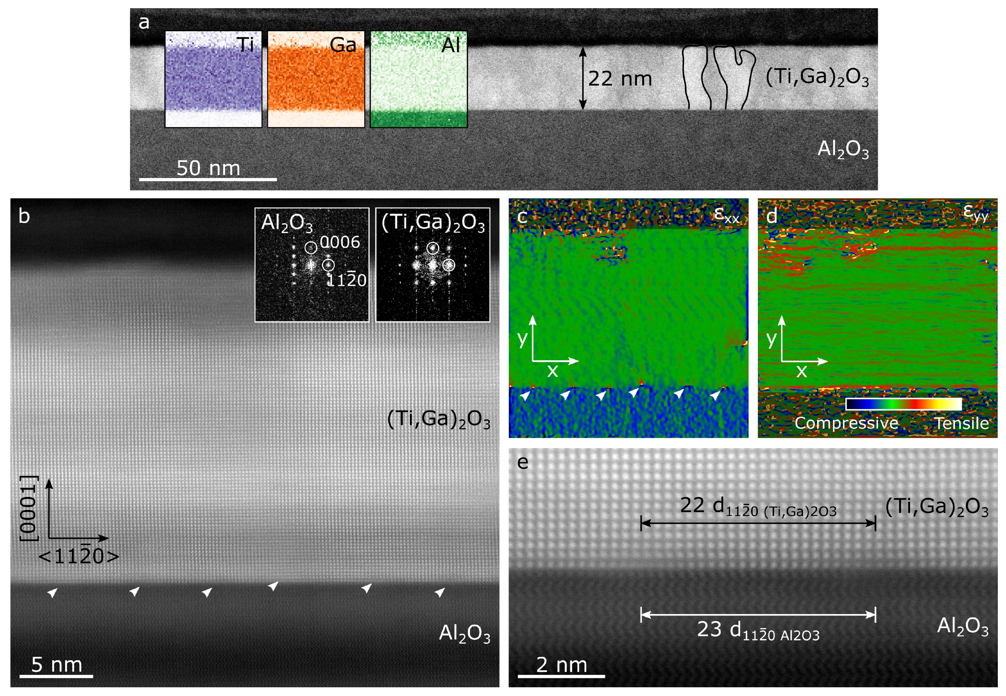
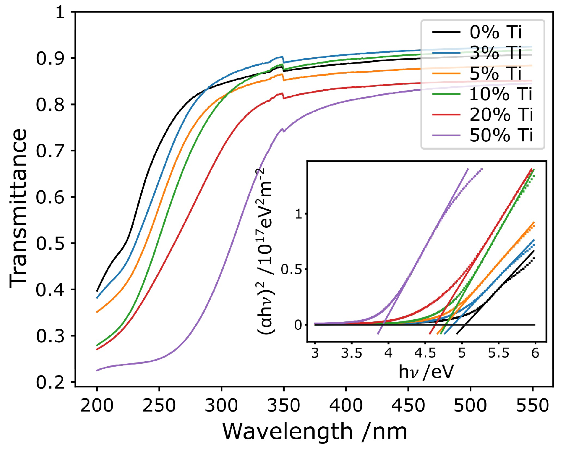
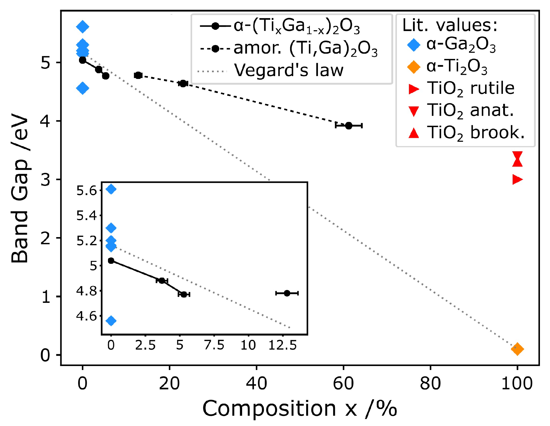
3. Results and Discussion
4. Conclusions
Author Contributions
Funding
Acknowledgments
Conflicts of Interest
References
- Shinohara, D.; Fujita, S. Heteroepitaxy of corundum-structured α-Ga2O3 thin films on α-Al2O3 substrates by ultrasonic mist chemical vapor deposition. Jpn. J. Appl. Phys. 2008, 47, 7311–7313. [Google Scholar] [CrossRef]
- Guo, D.; Zhao, X.; Zhi, Y.; Cui, W.; Huang, Y.; An, Y.; Li, P.; Wu, Z.; Tang, W. Epitaxial growth and solar-blind photoelectric properties of corundum-structured α-Ga2O3 thin films. Mater. Lett. 2016, 164, 364–367. [Google Scholar] [CrossRef]
- Oshima, Y.; Villora, E.G.; Shimamura, K. Halide vapor phase epitaxy of twin-free α-Ga2O3 on sapphire (0001) substrates. Appl. Phys. Express 2015, 8, 055501. [Google Scholar] [CrossRef]
- Lee, S.H.; Lee, K.M.; Kim, Y.B.; Moon, Y.J.; Kim, S.B.; Bae, D.; Kim, T.J.; Kim, Y.D.; Kim, S.K.; Lee, S.W. Sub-microsecond response time deep-ultraviolet photodetectors using α-Ga2O3 thin films grown via low-temperature atomic layer deposition. J. Alloys Compd. 2019, 780, 400–407. [Google Scholar] [CrossRef]
- Roberts, J.W.; Chalker, P.R.; Ding, B.; Oliver, R.A.; Gibbon, J.T.; Jones, L.A.H.; Dhanak, V.R.; Phillips, L.J.; Major, J.D.; Massabuau, F.C.P. Low temperature growth and optical properties of α-Ga2O3 deposited on sapphire by plasma enhanced atomic layer deposition. J. Cryst. Growth 2019, 528, 125254. [Google Scholar] [CrossRef]
- Zhao, X.; Wu, Z.; Guo, D.; Cui, W.; Li, P.; An, Y.; Li, L.; Tang, W. Growth and characterization of α-phase Ga2-xSnxO3 thin films for solar-blind ultraviolet applications. Semicond. Sci. Technol. 2016, 31, 065010. [Google Scholar] [CrossRef]
- Moloney, J.; Tesh, O.; Singh, M.; Roberts, J.; Jarman, J.; Lee, L.; Huq, T.; Brister, J.; Karboyan, S.; Kuball, M.; et al. Atomic layer deposited α-Ga2O3 solar-blind photodetectors. J. Phys. D Appl. Phys. 2019, 52, 475101. [Google Scholar] [CrossRef]
- Gross, A.; Stangl, F.; Hoenes, K.; Sift, M.; Hessling, M. Improved Drinking Water Disinfection with UVC-LEDs for Escherichia Coli and Bacillus Subtilis Utilizing Quartz Tubes as Light Guide. Water 2015, 7, 4605–4621. [Google Scholar] [CrossRef]
- Razeghi, M. Short-wavelength solar-blind detectors-status, prospects, and markets. Proc. IEEE 2002, 90, 1006–1014. [Google Scholar] [CrossRef]
- Roy, R.; Hill, V.G.; Osborn, E.F. Polymorphism of Ga2O3 and the System Ga2O3—H2O. J. Am. Chem. Soc. 1952, 74, 719–722. [Google Scholar] [CrossRef]
- Playford, H.Y.; Hannon, A.C.; Barney, E.R.; Walton, R.I. Structures of Uncharacterised Polymorphs of Gallium Oxide from Total Neutron Diffraction. Chem. A Eur. J. 2013, 19, 2803–2813. [Google Scholar] [CrossRef] [PubMed]
- Stepanov, S.I.; Nikolaev, V.I.; Bougrov, V.E.; Romanov, A.E. Gallium Oxide: Properties and Applications—A Review. Rev. Adv. Mater. Sci. 2016, 44, 63–86. [Google Scholar]
- Pearton, S.J.; Yang, J.; Cary, P.H.; Ren, F.; Kim, J.; Tadjer, M.J.; Mastro, M.A. A review of Ga2O3 materials, processing, and devices. Appl. Phys. Rev. 2018, 5, 011301. [Google Scholar] [CrossRef]
- Kaneko, K.; Kawanowa, H.; Ito, H.; Fujita, S. Evaluation of Misfit Relaxation in α-Ga2O3 Epitaxial Growth on α-Al2O3 Substrate. Jpn. J. Appl. Phys. 2012, 51, 020201. [Google Scholar] [CrossRef]
- Fujita, S.; Oda, M.; Kaneko, K.; Hitora, T. Evolution of corundum-structured III-oxide semiconductors: Growth, properties, and devices. Jpn. J. Appl. Phys. 2016, 55, 1202A3. [Google Scholar] [CrossRef]
- Roberts, J.W.; Jarman, J.; Johnstone, D.; Midgley, P.; Chalker, P.; Oliver, R.; Massabuau, F.C.P. α-Ga2O3 grown by low temperature atomic layer deposition on sapphire. J. Cryst. Growth 2018, 487, 23–27. [Google Scholar] [CrossRef]
- Wheeler, V.; Nepal, N.; Boris, D.; Qadri, S.; Nyakiti, L.; Lang, A.; Koehler, A.; Foster, G.; Walton, S.; Eddy, C., Jr.; et al. Phase Control of Crystalline Ga2O3 Films by Plasma-Enhanced Atomic Layer Deposition. Chem. Mater. 2020, 32, 1140. [Google Scholar] [CrossRef]
- Lee, S.D.; Ito, Y.; Kaneko, K.; Fujita, S. Enhanced thermal stability of alpha gallium oxide films supported by aluminum doping. Jpn. J. Appl. Phys. 2015, 54, 030301. [Google Scholar] [CrossRef]
- Kaneko, K.; Nomura, T.; Fujita, S. Corundum-structured α-phase Ga2O3-Cr2O3-Fe2O3 alloy system for novel functions. Phys. Status Solidi C 2010, 7, 2467–2470. [Google Scholar] [CrossRef]
- Kaneko, K.; Kakeya, I.; Komori, S.; Fujita, S. Band gap and function engineering for novel functional alloy semiconductors: Bloomed as magnetic properties at room temperature with α-phase (Ga,Fe)2O3. J. Appl. Phys. 2013, 113, 233901. [Google Scholar] [CrossRef]
- Wang, T.; Li, W.; Ni, C.; Janotti, A. Band Gap and Band Offset of Ga2O3 and (AlxGa1-x)2O3 alloys. Phys. Rev. Appl. 2018, 10, 011003. [Google Scholar] [CrossRef]
- Song, K.; Mohseni, M.; Taghipour, F. Application of ultraviolet light-emitting diodes (UV-LEDs) for water disinfection: A review. Water Res. 2016, 94, 341. [Google Scholar] [CrossRef] [PubMed]
- Smith, E. The emission spectrum of hydrocarbon flames. Proc. R. Soc. Lond. A 1940, 174, 110. [Google Scholar] [CrossRef]
- Ito, H.; Kaneko, K.; Fujita, S. Growth and Band Gap Control of Corundum-Structured α-(Al,Ga)2O3 Thin Films on Sapphire by Spray-Assisted Mist Chemical Vapor Deposition. Jpn. J. Appl. Phys. 2012, 51, 100207. [Google Scholar] [CrossRef]
- Fujita, S.; Kaneko, K. Epitaxial growth of corundum-structured wide bandgap III-oxide semiconductor thin films. J. Cryst. Growth 2014, 401, 588–592. [Google Scholar] [CrossRef]
- Kaneko, K.; Fujita, S.; Hitora, T. A power device material of corundum-structured α-Ga2O3 fabricated by MIST EPITAXY technique. Jpn. J. Appl. Phys. 2018, 57, 02CB18. [Google Scholar] [CrossRef]
- Innocenzi, M.E.; Swimm, R.T.; Bass, M.; French, R.H.; Villaverde, A.B.; Kokta, M.R. Room-temperature optical absorption in undoped α-Al2O3. J. Appl. Phys. 1990, 67, 7542–7546. [Google Scholar] [CrossRef]
- Weiher, R.L.; Ley, R.P. Optical Properties of Indium Oxide. J. Appl. Phys. 1966, 37, 299–302. [Google Scholar] [CrossRef]
- Chi, T.C.; Sladek, R.J. Elastic Constants and the Electrical Transition in Ti2O3. Phys. Rev. B 1973, 7, 5080–5085. [Google Scholar] [CrossRef]
- Li, Y.; Weng, Y.; Yin, X.; Yu, X.; Kumar, S.R.S.; Wehbe, N.; Wu, H.; Alshareef, H.N.; Pennycook, S.J.; Breese, M.B.H.; et al. Orthorhombic Ti2O3: A Polymorph-Dependent Narrow-Bandgap Ferromagnetic Oxide. Adv. Funct. Mater. 2018, 28, 1705657. [Google Scholar] [CrossRef]
- Guo, Y.; Clark, S.; Robertson, J. Calculation of metallic and insulating phases of V2O3 by hybrid density functionals. J. Chem. Phys. 2014, 140, 054702. [Google Scholar] [CrossRef] [PubMed]
- Al-Kuhaili, M.; Saleem, M.; Durrani, S. Optical properties of iron oxide (α-Fe2O3) thin films deposited by the reactive evaporation of iron. J. Alloys Compd. 2012, 521, 178–182. [Google Scholar] [CrossRef]
- Cheng, R.; Xu, B.; Borca, C.N.; Sokolov, A.; Yang, C.S.; Yuan, L.; Liou, S.H.; Doudin, B.; Dowben, P.A. Characterization of the native Cr2O3 oxide surface of CrO2. Appl. Phys. Lett. 2001, 79, 3122–3124. [Google Scholar] [CrossRef]
- Koffyberg, F.P. Optical bandgaps and electron affinities of semiconducting Rh2O3(I) and Rh2O3(III). J. Phys. Chem. Solids 1992, 53, 1285–1288. [Google Scholar] [CrossRef]
- Thomas, G.A.; Rapkine, D.H.; Carter, S.A.; Millis, A.J.; Rosenbaum, T.F.; Metcalf, P.; Honig, J.M. Observation of the Gap and Kinetic Energy in a Correlated Insulator. Phys. Rev. Lett. 1994, 73, 1529–1532. [Google Scholar] [CrossRef]
- Yao, Y.; Okur, S.; Lyle, L.A.M.; Tompa, G.S.; Salagaj, T.; Sbrockey, N.; Davis, R.F.; Porter, L.M. Growth and characterization of α-, β-, and ϵ-phases of Ga2O3 using MOCVD and HVPE techniques. Mater. Res. Lett. 2018, 6, 268–275. [Google Scholar] [CrossRef]
- Lee, W.E.; Lagerlof, K.P.D. Structural and electron diffraction data for sapphire (α-Al2O3). J. Electron Microsc. Tech. 1985, 2, 247–258. [Google Scholar] [CrossRef]
- Zhang, K.H.L.; Lazarov, V.K.; Galindo, P.L.; Oropeza, F.E.; Payne, D.J.; Lai, H.H.C.; Egdell, R.G. Domain Matching Epitaxial Growth of In2O3 Thin Films on α-Al2O3 (0001). Cryst. Growth Des. 2012, 12, 1000–1007. [Google Scholar] [CrossRef]
- Rice, C.E.; Robinson, W.R. Structural changes in the solid solution (Ti1-xVx)2O3 as x varies from zero to one. J. Solid State Chem. 1977, 21, 155–160. [Google Scholar] [CrossRef]
- Di Cerbo, R.K.; Seybolt, A.U. Lattice Parameters of the α-Fe2O3-Cr2O3 Solid Solution. J. Am. Ceram. Soc. 1959, 42, 430–431. [Google Scholar] [CrossRef]
- Coey, J.M.D. The crystal structure of Rh2O3. Acta Crystallogr. Sect. B Struct. Crystallogr. Cryst. Chem. 1970, 26, 1876–1877. [Google Scholar] [CrossRef]
- McWhan, D.B.; Remeika, J.P. Metal-Insulator Transition in (V1-xCrx)2O3). Phys. Rev. B 1970, 2, 3734–3750. [Google Scholar] [CrossRef]
- Mott, N. Metal-insulator transition in Ti2O3. J. Phys. 1981, 42, 277–281. [Google Scholar] [CrossRef]
- Manandhar, S.; Ramana, C. Direct, functional relationship between structural and optical properties in titanium-incorporated gallium oxide nanocrystalline thin films. Appl. Phys. Lett. 2017, 110, 061902. [Google Scholar] [CrossRef]
- Manandhar, S.; Battu, A.; Tan, S.; Panat, R.; Shutthanandan, V.; Ramana, C. Effect of Ti doping on the crystallography, phase, surface/interface structure and optical band gap of Ga2O3 thin films. J. Mater. Sci. 2019, 54, 11526. [Google Scholar] [CrossRef]
- Bandi, M.; Zade, V.; Roy, S.; Nair, A.; Seacat, S.; Sreenivasan, S.; Shutthanandan, S.; Van de Walle, C.; Peelaers, H.; Ramana, C. Effect of Titanium Induced Chemical Inhomogeneity on Crystal Structure, Electronic Structure, and Optical Properties of Wide Band Gap Ga2O3. Cryst. Growth Des. 2020, 20, 1422. [Google Scholar] [CrossRef]
- Ritala, M.; Leskela, M.; Niinisto, L.; Haussalo, P. Titanium isopropoxide as a precursor in atomic layer epitaxy of titanium dioxide thin films. Chem. Mater. 1993, 5, 1174–1181. [Google Scholar] [CrossRef]
- Mayer, M. SIMNRA User’s Guide for Version 7.0; Max-Planck-Institut für Plasmaphysik: Garching, Germany, 2017. [Google Scholar]
- Ernst Ruska-Centre for Microscopy and Spectroscopy with Electrons. J. Large-Scale Res. Facil. 2016, 2, A43. [CrossRef]
- Hÿtch, M.J.; Snoeck, E.; Kilaas, R. Quantitative measurement of displacement and strain fields from HREM micrographs. Ultramicroscopy 1998, 74, 131–146. [Google Scholar] [CrossRef]
- Mackus, A.J.M.; Schneider, J.R.; MacIsaac, C.; Baker, J.G.; Bent, S.F. Synthesis of Doped, Ternary, and Quaternary Materials by Atomic Layer Deposition: A Review. Chem. Mater. 2019, 31, 1142–1183. [Google Scholar] [CrossRef]
- Coll, M.; Napari, M. Atomic layer deposition of functional multicomponent oxides. APL Mater. 2019, 7, 110901. [Google Scholar] [CrossRef]
- Vegard, L. Die Konstitution der Mischkristalle und die Raumfüllung der Atome. Die Konstitution Der Mischkristal. Z. Phys. 1921, 5, 17. [Google Scholar] [CrossRef]
- Denton, A.R.; Ashcroft, N.W. Vegard’s law. Phys. Rev. A 1991, 43, 3161–3164. [Google Scholar] [CrossRef] [PubMed]
- Chen, Z.; Jaramillo, T. The Use of UV-Visible Spectroscopy to Measure the Band Gap of a Semiconductor; Department of Chemical Engineering, Stanford University: Stanford, CA, USA, 2017. [Google Scholar]
- Pascual, J.; Camassel, J.; Mathieu, H. Fine structure in the intrinsic absorption edge of TiO2. Phys. Rev. B 1978, 18, 5606–5614. [Google Scholar] [CrossRef]
- Amtout, A.; Leonelli, R. Optical properties of rutile near its fundamental band gap. Phys. Rev. B 1995, 51, 6842–6851. [Google Scholar] [CrossRef]
- Tang, H.; Levy, F.; Berger, H.; Schmid, P.E. Urbach tail of anatase TiO2. Phys. Rev. B 1995, 52, 7771–7774. [Google Scholar] [CrossRef]
- Mattsson, A.; Osterlund, L. Adsorption and Photoinduced Decomposition of Acetone and Acetic Acid on Anatase, Brookite, and Rutile TiO2 Nanoparticles. J. Phys. Chem. C 2010, 114, 14121–14132. [Google Scholar] [CrossRef]
- Hou, Y.; Wu, L.; Wang, X.; Ding, Z.; Li, Z.; Fu, X. Photocatalytic performance of α-, β-, and γ-Ga2O3 for the destruction of volatile aromatic pollutants in air. J. Catal. 2007, 250, 12–18. [Google Scholar] [CrossRef]
- Segura, A.; Artus, L.; Cusco, R.; Goldhahn, R.; Feneberg, M. Band gap of corundumlike α-Ga2O3 determined by absorption and ellipsometry. Phys. Rev. Mater. 2017, 1, 024604. [Google Scholar] [CrossRef]
- Shin, S.H.; Chandrashekhar, G.V.; Loehman, R.E.; Honig, J.M. Thermoelectric Effects in Pure and V-Doped Ti2O3 Single Crystals. Phys. Rev. B 1973, 8, 1364–1372. [Google Scholar] [CrossRef]


| Sample | Thickness/nm | Composition x/% | RMS Roughness/nm | Band Gap/eV |
|---|---|---|---|---|
| 0%Ti | 33 ± 3 | 0 | 0.71 ± 0.01 | ∼5.04 |
| 3%Ti | 22 ± 2 | 3.7 ± 0.4 | 0.49 ± 0.02 | ∼4.88 |
| 5%Ti | 21 ± 2 | 5.3 ± 0.4 | 0.30 ± 0.01 | ∼4.77 |
| 10%Ti | 21 ± 2 | 12.8 ± 0.8 | 0.22 ± 0.01 | ∼4.78 |
| 20%Ti | 21 ± 2 | 23.1 ± 1.0 | 0.19 ± 0.01 | ∼4.63 |
| 50%Ti | 16 ± 2 | 61 ± 3 | 0.16 ± 0.01 | ∼3.91 |
Publisher’s Note: MDPI stays neutral with regard to jurisdictional claims in published maps and institutional affiliations. |
© 2020 by the authors. Licensee MDPI, Basel, Switzerland. This article is an open access article distributed under the terms and conditions of the Creative Commons Attribution (CC BY) license (http://creativecommons.org/licenses/by/4.0/).
Share and Cite
Barthel, A.; Roberts, J.; Napari, M.; Frentrup, M.; Huq, T.; Kovács, A.; Oliver, R.; Chalker, P.; Sajavaara, T.; Massabuau, F. Ti Alloyed α-Ga2O3: Route towards Wide Band Gap Engineering. Micromachines 2020, 11, 1128. https://doi.org/10.3390/mi11121128
Barthel A, Roberts J, Napari M, Frentrup M, Huq T, Kovács A, Oliver R, Chalker P, Sajavaara T, Massabuau F. Ti Alloyed α-Ga2O3: Route towards Wide Band Gap Engineering. Micromachines. 2020; 11(12):1128. https://doi.org/10.3390/mi11121128
Chicago/Turabian StyleBarthel, Armin, Joseph Roberts, Mari Napari, Martin Frentrup, Tahmida Huq, András Kovács, Rachel Oliver, Paul Chalker, Timo Sajavaara, and Fabien Massabuau. 2020. "Ti Alloyed α-Ga2O3: Route towards Wide Band Gap Engineering" Micromachines 11, no. 12: 1128. https://doi.org/10.3390/mi11121128
APA StyleBarthel, A., Roberts, J., Napari, M., Frentrup, M., Huq, T., Kovács, A., Oliver, R., Chalker, P., Sajavaara, T., & Massabuau, F. (2020). Ti Alloyed α-Ga2O3: Route towards Wide Band Gap Engineering. Micromachines, 11(12), 1128. https://doi.org/10.3390/mi11121128