Application of Stereolithography Based 3D Printing Technology in Investment Casting


Abstract
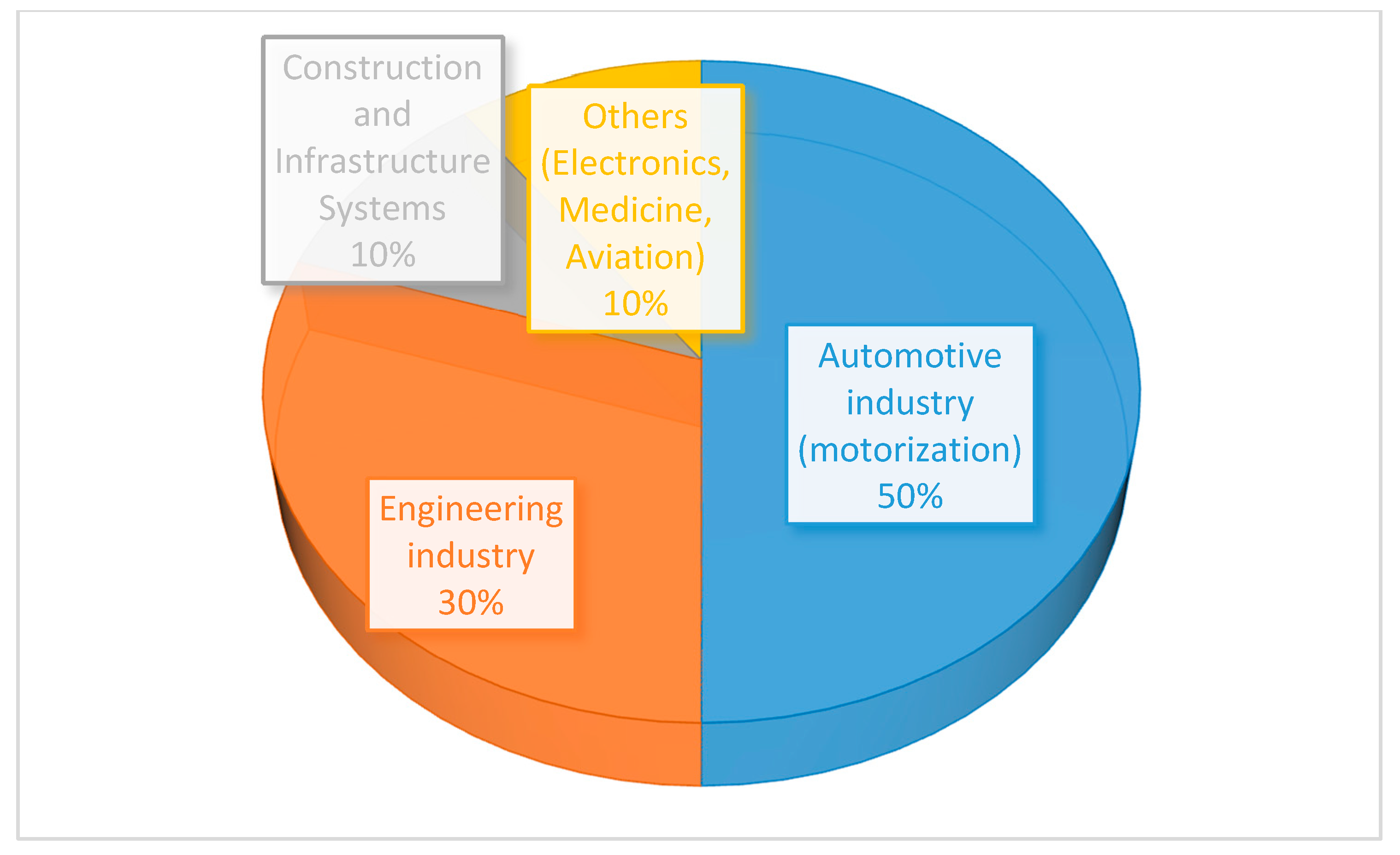
:1. Introduction
- During the design cycle engineers can make changes to the model without compromising manufacturing lead time;
- Prototypes are useful for verification and assembly design; the case study showed that every fourth design change was due to defects revealed by the prototype model;
- The assembly of RP models served design optimization that helped to ignore unnecessary engineering change notices. As a result, cycle time can be reduced greatly;
- Elimination of the cost requalification of casting. As casting is integrated into the first production phase, there is no need to perform mechanical testing of initially casted parts. Therefore, the new approach has less expenditures;
- Reduction of scrap, due to shortening of machining operation.
2. Role of Additive Manufacturing in IC
2.1. Fused Deposition Modeling
2.2. Selective Laser Sintering
2.3. 3D Printing (3DP)
2.4. Model Maker II
2.5. Laminated Object Manufacturing
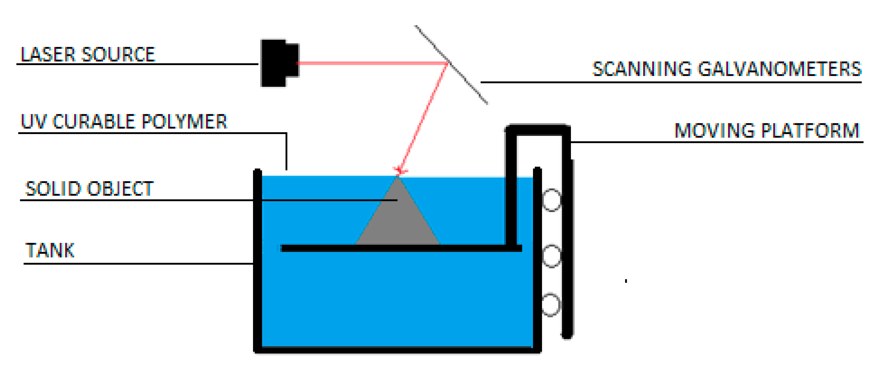
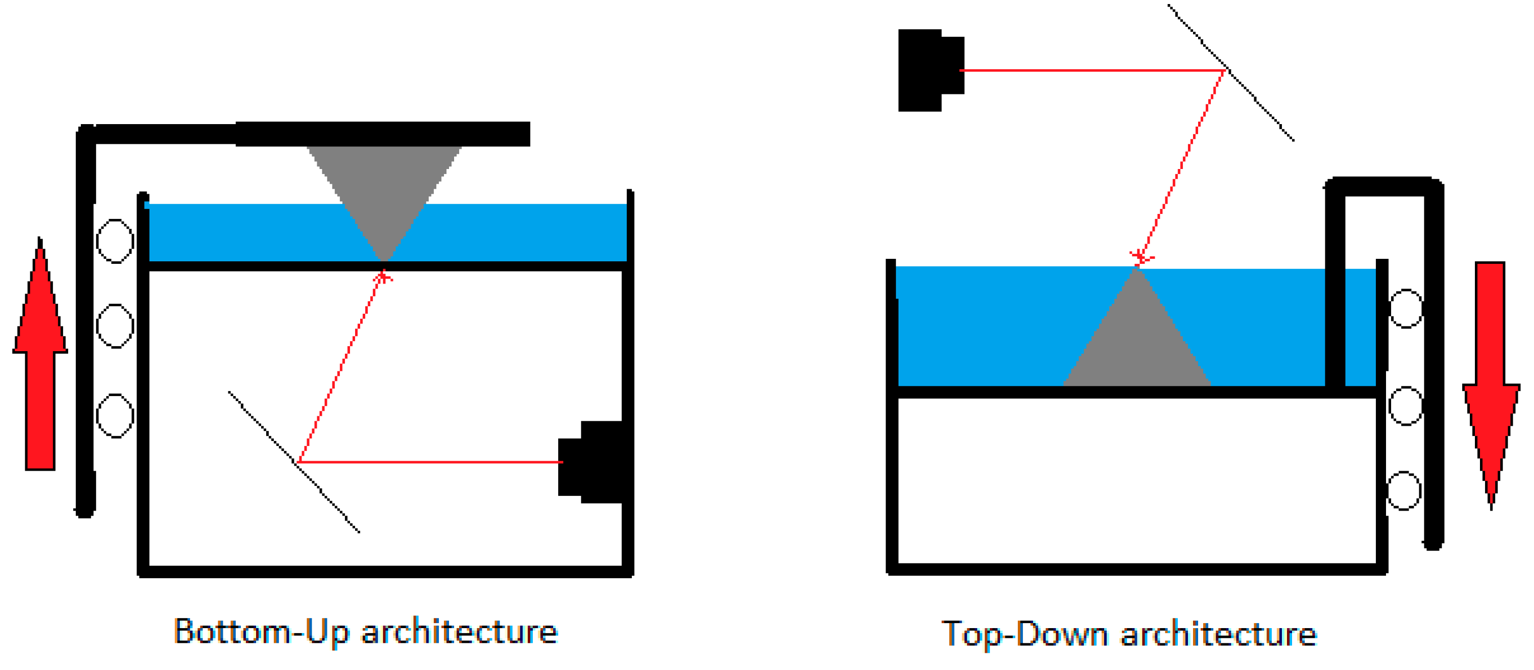
3. SLA Working Principle
- CAD model generation on any suitable software;
- STL file generation (3D meshes of triangular elements);
- SLI file generation (model slicing);
- Manufacturing layer by layer using SLA printer;
- Post processing (removing built supports, washing and curing).
4. Description of the Properties of Printed Parts that Are Important in IC
4.1. Dimensional Accuracy of SLA Printed Patterns
- The concave and convex surfaces of the turbine blade had an average deviation of 160 µm and 220 µm, for SLA and FDM, respectively.
- As for the wax pattern, the majority of deviations were within a 500 µm tolerance limit.
- It was also suggested that SLA is a better option in terms of dimensional accuracy and surface roughness, in comparison to the FDM method for silicon mold making process.
4.2. Surface Roughness of SLA Printed Parts
4.3. Mechanical Properties of SLA Printed Patterns
5. Photopolymers and Issues in SLA Technology
5.1. Free Radiacal and Cationic Systems
5.2. Non Polymer Materials Printed by SLA
- parts should undergo debinding and sintering steps after manufacturing;
- the viscosity of the suspension should be low enough for proper recoating to take place;
- the suspension should have a sufficient amount of powder to ensure the satisfactory mechanical properties of the product that has gone through rebinding and sintering;
- the curing depth and resolution must be appropriate; the presence of powder particles interfere in absorption of beam light by the polymer. Thus, the curing depth decreases, leading to an increase of processing time.
5.3. Ceramic Shell Cracking
6. Current Research Trends and Challenges
- The majority of research publications on the topic are ten or more years old, thus, new research projects are needed, which might investigate new materials, technologies, and machines currently available.
- The research is scarce on the application of SLA in indirect tooling.
- Limited publications are available on the performance of new polymers suitable for IC;
- An important constraint to the incorporation of RC in foundries is still the high cost of AM machines, building materials, and consumables. Therefore, it is important to search for means of making the manufacturing process more cost effective.
- The ceramic shell cracking phenomenon remains an issue for parts with thin walls and complicated shapes. Few ways of solving this problem have been proposed by researchers. The two main directions of investigations are materials and process based approaches.
- Although the dimensional accuracy of SLA printed parts is higher compared to most AM technologies, it is still inferior to conventional CNC machining.
- Surface roughness is critical in manufacturing precise aerospace and medical products. Therefore, these fields require very low surface roughness values. Like many AM processes, SLA is prone to having a stair stepping effect. Improving the surface quality of SLA printed parts can be achieved through improving process parameters and advancements in materials science. Thus, deep knowledge is required to identify the major parameters that affect the surface roughness.
- The toxicity level of widely used photopolymers should be studied to evaluate the level of risk and perform a proper life cycle analysis of SLA based IC process.
7. Conclusions
Author Contributions
Funding
Conflicts of Interest
References
- Holtzer, M.; Dańko, R.; Żymankowska-Kumon, S. Foundry industry–current state and future development. Metalurgija 2012, 51, 337–340. [Google Scholar]
- Kalpakjian, S.; Schmid, S.R. Manufacturing Engineering Technology; Dorling Kindersley Pvt Ltd.; Pearson Educ.: London, UK, 2009. [Google Scholar]
- Ingole, D.S.; Kuthe, A.M.; Thakare, S.B.; Talankar, A.S. Rapid prototyping–a technology transfer approach for development of rapid tooling. Rapid Prototyp. J. 2009, 15, 280–290. [Google Scholar] [CrossRef]
- Youssef, A.; Hollister, S.J.; Dalton, P.D. Additive manufacturing of polymer melts for implantable medical devices and scaffolds. Biofabrication 2017, 9, 12002. [Google Scholar] [CrossRef] [PubMed]
- Liu, R.; Wang, Z.; Sparks, T.; Liou, F.; Newkirk, J. Aerospace applications of laser additive manufacturing. In Laser Additive Manufacturing; Elsevier: Amsterdam, The Netherlands, 2017; pp. 351–371. [Google Scholar]
- Javaid, M.; Haleem, A. Current status and applications of additive manufacturing in dentistry: A literature-based review. J. Oral Biol. Craniofacial Res. 2019, 9, 179–185. [Google Scholar] [CrossRef] [PubMed]
- Evans, B. Practical 3D Printers: The Science and Art of 3D Printing; Apress: New York, NY, USA, 2012; ISBN 1430243937. [Google Scholar]
- Wohlers, T.T.; Caffrey, T. Wohlers Report 2014: 3D Printing and Additive Manufacturing State of the Industry Annual Worldwide Progress Report; Wohlers Associates Fort Collins: Fort Collins, CO, USA, 2014; ISBN 0991333209. [Google Scholar]
- Caffrey, T.; Ian Campbell, T.W. Wohlers Report 2016: Additive Manufacturing and 3d Printing State of the Industry Annual Worldwide Progress Report; Wohlers Associates: Fort Collins, CO, USA, 2016. [Google Scholar]
- Melchels, F.P.W. Celebrating three decades of stereolithography. Virtual Phys. Prototyp. 2012, 7, 173–175. [Google Scholar] [CrossRef]
- Ligon, S.C.; Liska, R.; Stampfl, J.; Gurr, M.; Mülhaupt, R. Polymers for 3D Printing and Customized Additive Manufacturing. Chem. Rev. 2017, 117, 10212–10290. [Google Scholar] [CrossRef] [PubMed] [Green Version]
- Jacobs, P.F. Rapid Prototyping & Manufacturing: Fundamentals of Stereolithography; Society of Manufacturing Engineers: Dearborn, MI, USA, 1992; ISBN 0872634256. [Google Scholar]
- Ferreira, J.C.; Mateus, A. A numerical and experimental study of fracture in RP stereolithography patterns and ceramic shells for investment casting. J. Mater. Process. Technol. 2003, 134, 135–144. [Google Scholar] [CrossRef]
- Mueller, T. Stereolithography-based prototyping: Case histories of applications in product development. In IEEE Technical Applications Conference and Workshops. Northcon/95. Conference Record; IEEE: Piscataway, NJ, USA, 1995; pp. 305–309. [Google Scholar]
- Raja, V.; Zhang, S. Rapid and cost-effective manufacturing of high-integrity aerospace components Rapid and cost-effective manufacturing of high-integrity aerospace components. Int. J. Adv. Manuf. Technol. 2006, 27, 759–773. [Google Scholar] [CrossRef]
- Debroy, T.; Mukherjee, T.; Milewski, J.O.; Elmer, J.W.; Ribic, B.; Blecher, J.J.; Zhang, W. Scientific, technological and economic issues in metal printing and their solutions. Nat. Mater. 2019, 18, 1026–1032. [Google Scholar] [CrossRef]
- Ngo, T.D.; Kashani, A.; Imbalzano, G.; Nguyen, K.T.Q.; Hui, D. Additive manufacturing (3D printing): A review of materials, methods, applications and challenges. Compos. Part B Eng. 2018, 143, 172–196. [Google Scholar] [CrossRef]
- Song, B.; Zhao, X.; Li, S.; Han, C.; Wei, Q.; Wen, S.; Liu, J.; Shi, Y. Differences in microstructure and properties between selective laser melting and traditional manufacturing for fabrication of metal parts: A review. Front. Mech. Eng. 2015, 10, 111–125. [Google Scholar] [CrossRef]
- Carneiro, V.H.; Rawson, S.D.; Puga, H.; Meireles, J.; Withers, P.J. Additive Manufacturing Assisted Investment Casting: A Low-Cost Method to Fabricate Periodic Metallic Cellular Lattices. Addit. Manuf. 2020, 33, 101085. [Google Scholar] [CrossRef]
- Rooks, B. Rapid tooling for casting prototypes. Assem. Autom. 2002, 22, 40–45. [Google Scholar] [CrossRef]
- Cheah, C.M.; Chua, C.K.; Lee, C.W.; Feng, C.; Totong, K. Rapid prototyping and tooling techniques: A review of applications for rapid investment casting. Int. J. Adv. Manuf. Technol. 2005, 25, 308–320. [Google Scholar] [CrossRef]
- Mahindru, D.V.; Mahendru, P.; Mahindru, V.; Mahendru, P. Review of Rapid Prototyping-Technology for the Future. Glob. J. Comput. Sci. Technol. 2013, 13, 27–38. [Google Scholar]
- Melnikova, R.; Ehrmann, A.; Finsterbusch, K. 3D printing of textile-based structures by Fused Deposition Modelling (FDM) with different polymer materials. In IOP Conference Series: Materials Science and Engineering; IOP Publishing: Bristol, UK, 2014; Volume: 62, p. 012018. [Google Scholar]
- Hafsa, M.N.; Ibrahim, M.; Wahab, M.S.; Zahid, M.S. Evaluation of FDM pattern with ABS and PLA material. Appl. Mech. Mater. 2014, 465–466, 55–59. [Google Scholar] [CrossRef]
- Kumar, P.; Ahuja, I.P.S.; Singh, R. Application of fusion deposition modelling for rapid investment casting—A review. Int. J. Mater. Eng. Innov. 2012, 3, 204–227. [Google Scholar] [CrossRef]
- Cannell, N.; Sabau, A.S. Predicting Pattern Tooling and Casting Dimensions for Investment Casting, Phase II.; Edison Materials Technology Center (EMTEC): Dayton, OH, USA, 2005. [Google Scholar]
- Note, Investment Casting with PolyCast TM. Available online: https://polymaker.com/Downloads/Application_Note/PolyCast_Application_Note_V1.pdf (accessed on 15 October 2020).
- Choudhari, C.M.; Patil, V.D. Product Development and its Comparative Analysis by SLA, SLS and FDM Rapid Prototyping Processes. In IOP Conference Series: Materials Science and Engineering; IOP Publishing: Bristol, UK, 2016; Volume: 149. [Google Scholar]
- Harun, W.S.W.; Safian, S.; Idris, M.H. Evaluation of ABS patterns produced from FDM for investment casting process. WIT Trans. Eng. Sci. 2009, 64, 319–328. [Google Scholar]
- Chhabra, M.; Singh, R. Rapid casting solutions: A review. Rapid Prototyp. J. 2011, 17, 328–350. [Google Scholar] [CrossRef]
- Sheoran, A.J.; Kumar, H. Fused Deposition modeling process parameters optimization and effect on mechanical properties and part quality: Review and reflection on present research. Mater. Today Proc. 2020, 21, 1659–1672. [Google Scholar] [CrossRef]
- Chohan, J.S.; Singh, R.; Boparai, K.S. Vapor smoothing process for surface finishing of FDM replicas. Mater. Today Proc. 2020, 26, 173–179. [Google Scholar] [CrossRef]
- Hongjun, L.; Zitian, F.; Naiyu, H.; Xuanpu, D. A note on rapid manufacturing process of metallic parts based on SLS plastic prototype. J. Mater. Process. Technol. 2003, 142, 710–713. [Google Scholar] [CrossRef]
- Dotchev, K.; Soe, S. Rapid manufacturing of patterns for investment casting: Improvement of quality and success rate. Rapid Prototyp. J. 2006, 12, 156–164. [Google Scholar] [CrossRef]
- Zhang, H.; Zhu, T.; Cao, S.; Shu, X.; Sun, B.; Hu, Y. 3DP System Development Based on Lnkjet Printer and its Experimental Research. Mach. Des. Manuf. 2012, 7 . Available online: http://en.cnki.com.cn/Article_en/CJFDTotal-JSYZ201207046.htm (accessed on 12 October 2020).
- Gill, S.S.; Kaplas, M. Efficacy of powder-based three-dimensional printing (3DP) technologies for rapid casting of light alloys. Int. J. Adv. Manuf. Technol. 2011, 52, 53–64. [Google Scholar] [CrossRef]
- Upadhyay, M.; Sivarupan, T.; El Mansori, M. 3D printing for rapid sand casting—A review. J. Manuf. Process. 2017, 29, 211–220. [Google Scholar] [CrossRef] [Green Version]
- Marwah, O.M.F.; Sharif, S.; Zainol, M.A.; Ibrahim, M.; Mohamad, E.J. 3D printer patterns evaluation for direct investment casting. Appl. Mech. Mater. 2014, 465–466, 1400–1403. [Google Scholar] [CrossRef]
- Seleznev, M.; Shulz, B.; Cornie, J.; Zhang, S.; Sachs, E.; Serdy, J.; Cima, M. Novel Near-Net-Shape Tool-Less Method for Manufacturing of Cast Metal Matrix Composites: Three-Dimensional Printing (3DP) of Ceramic Preforms Combined with Investment Casting Technology. SAE Trans. 2000, 109, 235–242. [Google Scholar] [CrossRef]
- Fischer, F. FDM and Polyjet 3D printing. Pop. Plast. Packag. 2015, 60. Available online: http://vdzmade.ca/file_uploads/FDM%20and%20Polyjet.pdf (accessed on 12 October 2020).
- Udroiu, R.; Braga, I.C. Polyjet technology applications for rapid tooling. In MATEC Web of Conferences; EDP Sciences: Les Ulis, France, 2017; Volume 112, p. 3011. [Google Scholar]
- Park, J.; Tari, M.J.; Hahn, H.T. Characterization of the laminated object manufacturing (LOM) process. Rapid Prototyp. J. 2000, 6, 36–50. [Google Scholar] [CrossRef]
- Hugo, P. Suitability of Layer Manufacturing Technologies for Rapid Tooling Development in Investment Casting. Ph.D. Dissertation, University of Stellenbosch, Stellenbosch, South Africa, 2008. [Google Scholar]
- Mueller, B.; Kochan, D. Laminated object manufacturing for rapid tooling and patternmaking in foundry industry. Comput. Ind. 1999, 39, 47–53. [Google Scholar] [CrossRef]
- Jacobs, P.F. QuickCast 1.1 and Rapid Tooling. In Proceedings of the 4th European Conference on Rapid Prototyping & Manufacturing, Belgirate, Italy, 13–15 June 1995; pp. 1–27. [Google Scholar]
- Jain, P.; Kuthe, A.M. Feasibility study of manufacturing using rapid prototyping: FDM approach. Procedia Eng. 2013, 63, 4–11. [Google Scholar] [CrossRef] [Green Version]
- Sood, A.K. Use of Fused Deposition Modeling Process in Investment Precision Casting and Risk of Using Selective Laser Sintering Process. 2012; pp. 1–5. Available online: https://www.idc-online.com/technical_references/pdfs/mechanical_engineering/USE%20OF%20FUSED%20DEPOSITION.pdf (accessed on 12 October 2020).
- van de Crommert, S.; Seitz, S.; Esser, K.K.; McAlea, K. Sand, die and investment cast parts via the SLS selective laser sintering process. In Rapid Prototyping and Flexible Manufacturing; International Society for Optics and Photonics: Washington, DC, USA, 1997; Volume 3102, pp. 95–105. [Google Scholar]
- Gojzewski, H.; Guo, Z.; Grzelachowska, W.; Ridwan, M.G.; Hempenius, M.A.; Grijpma, D.W.; Vancso, G.J. Layer-by-Layer Printing of Photopolymers in 3D: How Weak is the Interface? ACS Appl. Mater. Interfaces 2020, 12, 8908–8914. [Google Scholar] [CrossRef] [PubMed] [Green Version]
- Bártolo, P.J. Stereolithography: Materials, Processes and Applications; Springer Science & Business Media: Berlin/Heidelberg, Germany, 2011; ISBN 0387929045. [Google Scholar]
- Vaezi, M.; Seitz, H.; Yang, S. A review on 3D micro-additive manufacturing technologies. Int. J. Adv. Manuf. Technol. 2013, 67, 1721–1754. [Google Scholar] [CrossRef]
- Shoji, S.; Smith, N.; Kawata, S. Photofabrication of a photonic crystal using interference of a UV laser. In Optical Engineering for Sensing and Nanotechnology (ICOSN’99); International Society for Optics and Photonics: Washington, DC, USA, 1999; Volume 3740, pp. 541–544. [Google Scholar]
- Ikuta, K.; Hasegawa, T.; Adachi, T. The optimized SMA micro pump chip applicable to liquids and gases. In Transducers’ 01 Eurosensors XV.; Springer: Berlin/Heidelberg, Germany, 2001; pp. 888–891. [Google Scholar]
- Bertsch, A.; Jiguet, S.; Bernhard, P.; Renaud, P. Microstereolithography: A Review; Swiss Federal Institute of Technology Lausanne: Lausanne, Switzerland, 2003. [Google Scholar]
- Han, D.; Lu, Z.; Chester, S.A.; Lee, H. Micro 3D printing of a temperature-responsive hydrogel using projection micro-stereolithography. Sci. Rep. 2018, 8, 1–10. [Google Scholar] [CrossRef]
- Lee, S.H.; Park, W.S.; Cho, H.S.; Zhang, W.; Leu, M.-C. A neural network approach to the modelling and analysis of stereolithography processes. Proc. Inst. Mech. Eng. Part B J. Eng. Manuf. 2001, 215, 1719–1733. [Google Scholar] [CrossRef]
- Zakeri, S.; Vippola, M.; Levänen, E. A comprehensive review of the photopolymerization of ceramic resins used in stereolithography. Addit. Manuf. 2020, 35, 101177. [Google Scholar] [CrossRef]
- Pham, D.T.; Dimov, S.S.; Gault, R.S. Part orientation in stereolithography. Int. J. Adv. Manuf. Technol. 1999, 15, 674–682. [Google Scholar] [CrossRef]
- Narahara, H.; Tanaka, F.; Kishinami, T.; Igarashi, S.; Saito, K. Reaction heat effects on initial linear shrinkage and deformation in stereolithography. Rapid Prototyp. J. 1999, 5, 120–128. [Google Scholar] [CrossRef]
- Bernhard, P.; Hofmann, M.; Schulthess, A.; Steinmann, B. Taking lithography to the third dimension. Chim. Int. J. Chem. 1994, 48, 427–430. [Google Scholar]
- Huang, Y.-M.; Lan, H.-Y. Compensation of distortion in the bottom exposure of stereolithography process. Int. J. Adv. Manuf. Technol. 2006, 27, 1101–1112. [Google Scholar] [CrossRef]
- Jayanthi, S.; Keefe, M.; Gargiulo, E.P. Studies in Stereolithography: Influence of Process Parameters on Curl Distortion in Photopolymer Models. In Proceedings of the 1994 International Solid Freeform Fabrication Symposium, Austin, TX, USA, 8–10 August 1994. [Google Scholar]
- Hull, C.W.; Spence, S.T.; Lewis, C.W.; Vinson, W.; Freed, R.S.; Smalley, D.R. Stereolithographic Curl reducTion. U.S. Patent No. 5,273,691, 28 December 1993. [Google Scholar]
- Salmoria, G.V.; Ahrens, C.H.; Beal, V.E.; Pires, A.T.N.; Soldi, V. Evaluation of post-curing and laser manufacturing parameters on the properties of SOMOS 7110 photosensitive resin used in stereolithography. Mater. Des. 2009, 30, 758–763. [Google Scholar] [CrossRef]
- Fadel, G.M.; Kirschman, C. Accuracy issues in CAD to RP translations. Rapid Prototyp. J. 1996, 2, 4–17. [Google Scholar] [CrossRef]
- Xu, G.; Jin, J.; Luo, S.; Qiu, R.; Pan, H. Research on Optimizing Build Parameters for Stereolithography Technology. In Proceedings of the 2009 International Conference on Measuring Technology and Mechatronics Automation, Zhangjiajie, China, 11–12 April 2009; Volume 2, pp. 883–886. [Google Scholar]
- Cheng, W.; Fuh, J.Y.H.; Nee, A.Y.C.; Wong, Y.S.; Loh, H.T.; Miyazawa, T. Multi-objective optimization of part-building orientation in stereolithography. Rapid Prototyp. J. 1995, 1, 12–23. [Google Scholar] [CrossRef]
- Yarlagadda, P.K.D.V.; Hock, T.S. Statistical analysis on accuracy of wax patterns used in investment casting process. J. Mater. Process. Technol. 2003, 138, 75–81. [Google Scholar] [CrossRef]
- Tewo, R.K.; Rutto, H.L.; Focke, W.; Seodigeng, T.; Koech, L.K. Formulations, development and characterization techniques of investment casting patterns. Rev. Chem. Eng. 2019, 35, 335–349. [Google Scholar] [CrossRef]
- Norouzi, Y.; Rahmati, S.; Hojjat, Y. A Novel Lattice Structure for SL Investment Casting Patterns. Rapid Prototyp. J. 2009, 15, 255–263. [Google Scholar] [CrossRef]
- Wohlers Associates Inc. Wohler’s report 2015—3D Printing and Additive Manufacturing State of the Industry. Annual Worldwide Progress Report; Wohlers Associates Inc.: Fort Collins, CO, USA, 2015; pp. 32–42. [Google Scholar]
- Pang, T.H. Stereolithography Epoxy Resin Development: Accuracy and Dimensional Stability. In Proceedings of the 1993 International Solid Freeform Fabrication Symposium, Austin, TX, USA, 9–11 August 1993. [Google Scholar]
- Jacobs, P. Stereolithography 1993: Epoxy resins, improved accuracy, and investment casting. Coupling Technol. Natl. Need 1994, 2102, 41–52. [Google Scholar]
- Queiroz, D.A.; Cunha, L.G.; Duarte, J.L.P.; Neves, A.C.C.; da Silva-Concílio, L.R. Influence of the casting material on the dimensional accuracy of dental dies. Braz. Oral Res. 2011, 25, 357–361. [Google Scholar] [CrossRef] [Green Version]
- Jacobs, P. Rapid tooling. World Cl. Des. to Manuf. 1995, 2, 42–50. [Google Scholar] [CrossRef]
- Tumbleston, J.R.; Shirvanyants, D.; Ermoshkin, N.; Janusziewicz, R.; Johnson, A.R.; Kelly, D.; Chen, K.; Pinschmidt, R.; Rolland, J.P.; Ermoshkin, A. Continuous liquid interface production of 3D objects. Science 2015, 347, 1349–1352. [Google Scholar] [CrossRef]
- Wu, H.; Li, D.; Tang, Y.; Guo, N.; Cui, F.; Sun, B. Rapid casting of hollow turbine blades using integral ceramic moulds. Proc. Inst. Mech. Eng. Part B J. Eng. Manuf. 2009, 223, 695–702. [Google Scholar] [CrossRef]
- Relvas, C.; Ramos, A.; Completo, A.; Simões, J.A. A systematic approach for an accuracy level using rapid prototyping technologies. Proc. Inst. Mech. Eng. Part B J. Eng. Manuf. 2012, 226, 2023–2034. [Google Scholar] [CrossRef]
- Rahmati, S.; Akbari, J.; Barati, E. Dimensional accuracy analysis of wax patterns created by RTV silicone rubber molding using the Taguchi approach. Rapid Prototyp. J. 2007, 13, 115–122. [Google Scholar] [CrossRef]
- Budzik, G. Properties of made by different methods of RP impeller foundry patterns. Arch. Foundry Eng. 2007, 7, 83–86. [Google Scholar]
- Iftikhar, A.; Khan, M.; Alam, K.; Imran Jaffery, S.H.; Ali, L.; Ayaz, Y.; Khan, A. Turbine blade manufacturing through rapid tooling (RT) process and its quality inspection. Mater. Manuf. Process. 2013, 28, 534–538. [Google Scholar] [CrossRef]
- Unkovskiy, A.; Bui, P.H.B.; Schille, C.; Geis-Gerstorfer, J.; Huettig, F.; Spintzyk, S. Objects build orientation, positioning, and curing influence dimensional accuracy and flexural properties of stereolithographically printed resin. Dent. Mater. 2018, 34, e324–e333. [Google Scholar] [CrossRef] [PubMed]
- Khaledi, A.-A.; Farzin, M.; Akhlaghian, M.; Pardis, S.; Mir, N. Evaluation of the marginal fit of metal copings fabricated by using 3 different CAD-CAM techniques: Milling, stereolithography, and 3D wax printer. J. Prosthet. Dent. 2020, 124, 81–86. [Google Scholar] [CrossRef] [PubMed]
- Islam, M.N.; Gomer, H.; Sacks, S. Comparison of dimensional accuracies of stereolithography and powder binder printing. Int. J. Adv. Manuf. Technol. 2017, 88, 3077–3087. [Google Scholar] [CrossRef]
- Yang, Q.; Lu, Z.; Zhou, J.; Miao, K.; Li, D. A novel method for improving surface finish of stereolithography apparatus. Int. J. Adv. Manuf. Technol. 2017, 93, 1537–1544. [Google Scholar] [CrossRef]
- Williams, R.E.; Melton, V.L. Abrasive flow finishing of stereolithography prototypes. Rapid Prototyp. J. 1998, 4, 56–67. [Google Scholar] [CrossRef]
- Jacobs, P.F. Stereolithography and other RP&M Technologies: From Rapid Prototyping to Rapid Tooling; Society of Manufacturing Engineers: Dearborn, MI, USA, 1995; ISBN 0872634671. [Google Scholar]
- Zhou, J.G.; Herscovici, D.; Chen, C.C. Parametric process optimization to improve the accuracy of rapid prototyped stereolithography parts. Int. J. Mach. Tools Manuf. 2000, 40, 363–379. [Google Scholar] [CrossRef]
- Arnold, C.; Monsees, D.; Hey, J.; Schweyen, R. Surface quality of 3D-printed models as a function of various printing parameters. Materials 2019, 12, 1970. [Google Scholar] [CrossRef] [Green Version]
- Sitek, P.W.-M.R.; Bolek, J.Z.; Mizera, J.; Kurzydlowski, K.J. A Study on Technological Properties of Investment Casting Waxes. Adv. Appl. Plasma Sci. 2015, 10, 37–40. [Google Scholar]
- Chantarapanich, N.; Puttawibul, P.; Sitthiseripratip, K.; Sucharitpwatskul, S.; Chantaweroad, S. Study of the mechanical properties of photo-cured epoxy resin fabricated by stereolithography process. Songklanakarin J. Sci. Technol 2013, 35, 91–98. [Google Scholar]
- Olayan, H.B.; Hami, H.S.; Owen, E.D. Photochemical and thermal crosslinking of polymers. J. Macromol. Sci. Part C Polym. Rev. 1996, 36, 671–719. [Google Scholar] [CrossRef]
- Bagheri, A.; Jin, J. Photopolymerization in 3D Printing. ACS Appl. Polym. Maters. 2019, 1, 593–611. [Google Scholar] [CrossRef] [Green Version]
- Decker, C.; Viet, T.N.T.; Decker, D.; Weber-Koehl, E. UV-radiation curing of acrylate/epoxide systems. Polymer (Guildf) 2001, 42, 5531–5541. [Google Scholar] [CrossRef]
- Wang, F.; Wang, F. Liquid Resins-Based Additive Manufacturing. J. Mol. Eng. Mater. 2017, 5, 1740004. [Google Scholar] [CrossRef]
- Bartolo, P.J.; Gaspar, J. Metal filled resin for stereolithography metal part. CIRP Ann. Manuf. Technol. 2008, 57, 235–238. [Google Scholar] [CrossRef]
- Kaczmarek, H. Effect of Irgacure 651 Initiator on Poly(Methyl Methacrylate) Photostability Studied by UV-Vis Spectroscopy. Open Process Chem. J. 2013, 1, 8–11. [Google Scholar] [CrossRef] [Green Version]
- Green, W.A. Industrial Photoinitiators: A Technical Guide; CRC Press: Boca Raton, FL, USA, 2010; ISBN 143982746X. [Google Scholar]
- A New Photoinitiator for Cationic Curing from Ciba Specialty Chemicals. Available online: https://www.chemeurope.com/en/news/10417/a-new-photoinitiator-for-cationic-curing-from-ciba-specialty-chemicals.html (accessed on 12 October 2020).
- Zhang, J.; Xiao, P. 3D printing of photopolymers. Polym. Chem. 2018, 9, 1530–1540. [Google Scholar] [CrossRef]
- Barner-Kowollik, C.; Bastmeyer, M.; Blasco, E.; Delaittre, G.; Müller, P.; Richter, B.; Wegener, M. 3D laser micro-and nanoprinting: Challenges for chemistry. Angew. Chemie Int. Ed. 2017, 56, 15828–15845. [Google Scholar] [CrossRef]
- Weng, Z.; Zhou, Y.; Lin, W.; Senthil, T.; Wu, L. Structure-property relationship of nano enhanced stereolithography resin for desktop SLA 3D printer. Compos. Part A Appl. Sci. Manuf. 2016, 88, 234–242. [Google Scholar] [CrossRef]
- Malshe, H.; Nagarajan, H.; Pan, Y.; Haapala, K. Profile of Sustainability in Additive Manufacturing and Environmental Assessment of a Novel Stereolithography Process. In International Manufacturing Science and Engineering Conference; American Society of Mechanical Engineers: New York, NY, USA, 2015; Volume 2, pp. 1–11. [Google Scholar]
- Brady, G.A.; Chu, T.-M.; Halloran, J.W. Curing behavior of Ceramic Resin for Stereolithography. In Proceedings of the 1996 International Solid Freeform Fabrication Symposium, Austin, TX, USA, 12–14 August 1996. [Google Scholar]
- Chartier, T.; Chaput, C.; Doreau, F.; Loiseau, M. Stereolithography of structural complex ceramic parts. J. Mater. Sci. 2002, 37, 3141–3147. [Google Scholar] [CrossRef]
- Zhou, W.; Li, D.; Wang, H. A novel aqueous ceramic suspension for ceramic stereolithography. Rapid Prototyp. J. 2010, 16, 29–35. [Google Scholar] [CrossRef]
- Griffith, M.L.; Halloran, J.W. Freeform Fabrication of Ceramics via Stereolithography. J. Am. Ceram. Soc. 2005, 79, 2601–2608. [Google Scholar] [CrossRef] [Green Version]
- Corcione, C.E.; Greco, A.; Montagna, F.; Licciulli, A.; Maffezzoli, A. Silica moulds built by stereolithography. J. Mater. Sci. 2005, 40, 4899–4904. [Google Scholar] [CrossRef]
- Bian, W.; Li, D.; Lian, Q.; Zhang, W.; Zhu, L.; Li, X.; Jin, Z. Design and fabrication of a novel porous implant with pre-set channels based on ceramic stereolithography for vascular implantation. Biofabrication 2011, 3, 1–7. [Google Scholar] [CrossRef]
- Zhu, J.-H.; Li, Q.; Zhang, W.-H. The periodic resin configuration design for ceramic-resin composite structure using topology optimization. Int. J. Simul. Multidiscip. Des. Optim. 2014, 5, A12. [Google Scholar] [CrossRef] [Green Version]
- Hague, R.; Dickens, P.M. Requirements for the Successful Autoclaving of Stereolithography Models in the Investment Casting Process. In Proceedings of the Second National Conference on Rapid Prototyping and Tooling Research, High Wycombe, UK, 18–19 November 1996; pp. 77–92. [Google Scholar]
- Hague, R.; Dickens, P.M. Improvements in investment casting with stereolithography patterns. Proc. Inst. Mech. Eng. Part B J. Eng. Manuf. 2001, 215, 1–11. [Google Scholar] [CrossRef]
- Wang, D.; Dong, A.; Zhu, G.; Shu, D.; Sun, J.; Li, F.; Sun, B. Rapid casting of complex impeller based on 3D printing wax pattern and simulation optimization. Int. J. Adv. Manuf. Technol. 2019, 100, 2629–2635. [Google Scholar] [CrossRef]
- Li, H.; Chandrashekhara, K.; Komaragiri, S.; Lekakh, S.N.; Richards, V.L. Crack prediction using nonlinear finite element analysis during pattern removal in investment casting process. J. Mater. Process. Technol. 2014, 214, 1418–1426. [Google Scholar] [CrossRef]
- Yao, W.L.; Leu, M.C. Analysis of shell cracking in investment casting with laser stereolithography patterns. Rapid Prototyp. J. 1999, 5, 12–20. [Google Scholar] [CrossRef]
- Zhao, H.; Xu, M.; Li, H.; Everhart, W.; Lekakh, S.; Richards, V.; Chandrashekhara, K.; Nam, P. Characterization of Low Density Polymer Patterns for Large Steel Investment Casting. In Proceedings of the Investment Casting Institute 58th Technical Conference & Equipment Expo, Covington, KY, USA, 10–11 October 2011; pp. 1–13. [Google Scholar]
- Li, Q.; Zhu, J.H.; Zhang, Y.H.; Zhang, W.H. The topology optimization of ceramic-resin composite structure under thermal and mechanical loads. Appl. Mech. Mater. 2013, 341, 124–128. [Google Scholar] [CrossRef]
- Komaragiri, S.; Li, H.; Lekakh, S.; Chandrashekhara, K.; Richards, V. Effects of complex geometry, shell thickness and firing regimes on shell cracking in industrial investment casting shells during rigid polymer pattern removal. In Proceedings of the CastExpo and the Metalcasting Congress, St. Louis, MO, USA, 6–9 April 2013. [Google Scholar]
- Chen, X.; Li, D.; Wu, H.; Tang, Y.; Zhao, L. Analysis of ceramic shell cracking in stereolithography-based rapid casting of turbine blade. Int. J. Adv. Manuf. Technol. 2011, 55, 447–455. [Google Scholar] [CrossRef]
- Harun, Z.; Kamarudin, N.H.; Ibrahim, M.; Idris, M.I.; Ahmad, S. Reinforced green ceramic shell mould for investment casting process. In Advanced Materials Research; Trans Tech Publications Ltd.: Stafa-Zurich, Switzerland, 2015; Volume 1087, pp. 415–419. [Google Scholar]
- Lu, Z.L.; Fan, Y.X.; Miao, K.; Jing, H.; Li, D.C. Effects of adding aluminum oxide or zirconium oxide fibers on ceramic molds for casting hollow turbine blades. Int. J. Adv. Manuf. Technol. 2014, 72, 873–880. [Google Scholar] [CrossRef]
- Jones, S.; Yuan, C. Advances in shell moulding for investment casting. J. Mater. Process. Technol. 2003, 135, 258–265. [Google Scholar] [CrossRef]
- Dougherty, T.K.; Elias, W.E.; Thelander, T.C.; Bhavnani, M.N. Resin Composition and Process for Investment Casting Using Stereolithography. U.S. Patent No. 5,391,460, 21 February 1995. [Google Scholar]
- Murphy, E.J.; Ansel, R.E.; Krajewski, J.J. Investment Casting Utilizing Patterns Produced by Stereolithography. U.S. Patent No. 4,844,144, 4 July 1989. [Google Scholar]


| Features Compared | Casting with Stereolithography (SLA) | Traditional Wax Pattern | Machining from Stock Material |
|---|---|---|---|
| Cost, thousands of $ | 215 | 330 | 550 |
| Cycle time, months | 5 | 8 | 7 |
| Length of time for incorporating design changes, months | 2 | 1 | 1 |
| Type of AM | Advantages | Disadvantages | Source |
|---|---|---|---|
| SLA | High dimensional accuracy and fine detail; high quality surface finish; wide range of materials can be printed including wax and non-wax; relatively fast; low cost of desktop machines; transparent parts. | High cost of consumables; resin drainage of thin walled parts is a challenge; working with QuickCast technology requires experience; post-processing is required. | [15,21,30,45] |
| FDM | Both wax and non-wax patterns can be printed; strong non-wax parts can be handled easily; high printing speed; can print thin walls; large variety of machine configurations with comparatively low cost; low cost of consumables. | Poor surface finish; high melting temperature of Acrylonitrile butadiene styrene (ABS); to achieve high surface finish and high dimensional accuracy, many process parameters, layer thickness being the most prominent, need to be adjusted, which leads to long printing time. | [21,25,30,46] |
| SLS | Surface roughness close to SLA; high speed of printing; using polystyrene based Windform material allows casting of highly reactive alloys; easy post processing and removal of support structures when using True Form PM material. | High thermal expansion when using Duraform material; low dimensional accuracy with polystyrene material; incapability of using only a portion of printing bed; high cost of powder. | [21,30,33,34,47,48] |
| 3DP | Low cost; very high speed of printing | Very low level of accuracy; poor surface finish. | [30,35,36] |
| Model Maker II | Can produce wax patterns; high quality of surface finish; no shell cracking. | Slow printing speed; fragility of wax material. | [21,30] |
| LOM | Low cost; high speed. | Low dimensional accuracy; inferior surface quality; more suitable for sand casting. | [25,44] |
| Defect Type | Caused by |
|---|---|
| Shrinkage | Forming large molecules from small ones during the polymerization process; post-curing of the liquid resin trapped in the lattice structure [12]. Reaction related heat: ceasing of the initial photo-polymerization reaction causes temperature decrease [59]. |
| Curl distortion | Curing process of each layer produces flexure of the layers previously solidified [56,60]. The part’s surface closest to the bottom of the platform curls most [61]. Layer thickness, hatch spacing, fill cure depth, and hatch over-cure [62]. |
| Warping | Insufficient polymerization leading to relaxation, diffusion, and evaporation of low molecular weight components [50]. Instantaneous increase in temperature and subsequent release of heat to the surroundings [63]. |
| Distortions Dimensional inaccuracy | Liberation of internal forces that have developed during the building process between the model and the platform [56] Resin’s photosensitivity characteristics and laser power [64]. Deviation of the laser beam when curing resin far from the platform center [65]. Hatch spacing, scanning speed and coefficient of the resin’s shrinkage compensation are the most influential parameters affecting dimensional accuracy [66]. Incorrect selection of part orientation [67]. |
| Year | Innovation |
|---|---|
| 1986 | 3D Systems Company founder Chuck Hull receives his patent for the first SLA apparatus [71] |
| 1988 | 3D Systems with its partner Ciba-Geigy introduced the first-generation acrylate resins. The resins had issues such as high viscosity, dimensional inconsistency, low strength, and brittleness [72] |
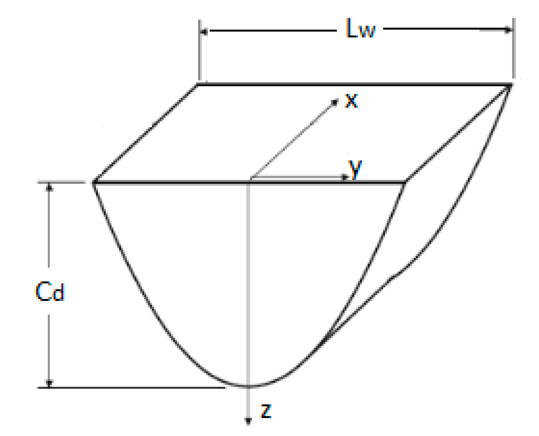
| 1993 | Commercialization of the first XB 5170 epoxy resin product. Despite the slowing down of photo-speed process, introducing epoxy/acrylate hybrids allowed lowering viscosity and improving both green and impact strengths [73,74]. Emergence of QuickCast 1.0 technology. The QuickCast innovation allows implementing a build style that makes inner the volume of pattern walls have a porous structure. Due to a considerable decrease in density of quasi-hollow parts, the inner part of pattern walls collapse before ceramic shell cracks [75]. As a result, the effect of polymer thermal expansion is almost eliminated [21]. Moreover, as less material is needed for printing hollow-like structures, material savings are another benefit of applying the QuickCast method. |
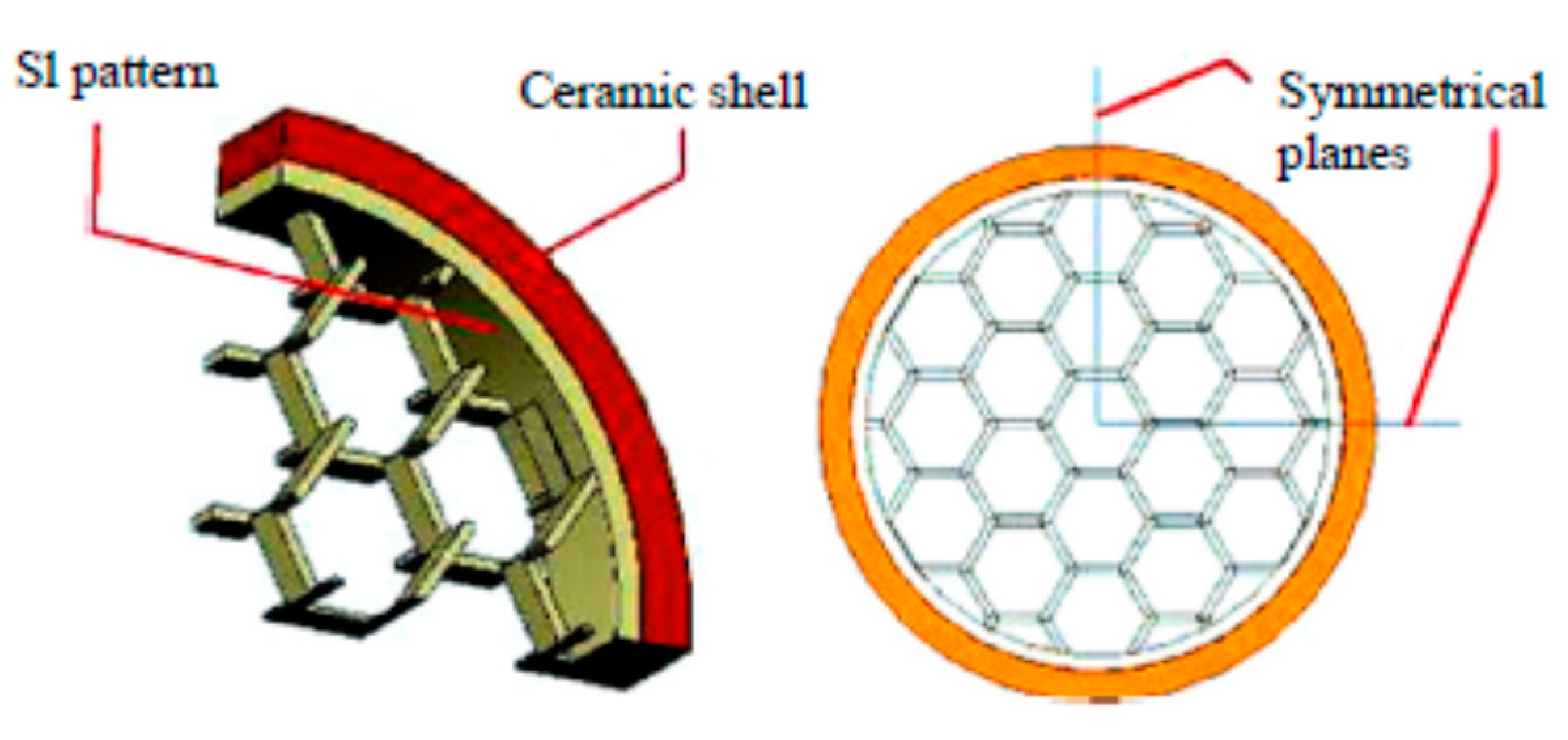
| 2000 | Through further development of QuickCast technology, new building styles have been introduced. For example, Figure 8 shows the hexagonal build style model of QuickCast 2.0. The superiority of QuickCast 2 over the previous version was in the reduction of shell stress by 2/3 [30]. |
| 2012 | First desktop printers under $5000 arrived on the market. |
| 2015 | Introduction of a new continuous liquid interface production system that significantly increased the printing speed. The system has a new oxygen permeable vat bottom, which allows continuous polymerization of the resin and elimination of the recoating step [76]. |
| Mean Values, mm | 3D Designed Value, mm | 0° Build Orientation | 45° Build Orientation | 90° Build Orientation |
|---|---|---|---|---|
| Height (x) | 5 | 4.5 (SD* = 0.11) | 4.9 (SD = 0.02) | 4.96 (SD = 0.01) |
| Wight (y) | 5 | 5.11 (SD = 0.06) | 4.82 (SD = 0.01) | 4.95 (SD = 0.01) |
| Length (z) | 30 | 29.94 (SD = 0.05) | 29.89 (SD = 0.03) | 29.25 (SD = 0.08) |
| Input Parameters | Unit | SLA | ||||
|---|---|---|---|---|---|---|
| Height | Height | Hole Dia. | Outer Dia. | Outer Dia. | ||
| Design size | mm | 10 | 60 | 30 | 46 | 126 |
| Measured mean size | mm | 10.367 | 59.995 | 29.859 | 45.768 | 125.394 |
| Dimensional error | µm | 367 | −5 | −141 | −232 | −606 |
| Type of Deviation | Total Number of Tested Elements | Number of Elements that Failed to Meet Tolerance Order of ISO2768-mk |
|---|---|---|
| Deviation of the linear dimensions | 6 | 3 |
| Deviation of radius, diameters, and angles | 16 | 5 |
| Geometric deviation of flatness and cylindricity | 17 | 5 |
| Geometric deviation of perpendicularity, coaxiality, parallelism, position, and angularity | 21 | 20 |
| Parameter | Effect |
|---|---|
| Layer thickness or resolution | Finer layer thickness results in a low value of Ra [87] |
| Blade gap | Medium blade gap is desirable, 0.005 inch [88] |
| Hatch space | Medium or low is preferable [88] |
| Position on the platform | The closer to the center the better [88] |
| Polymer | Properties | System Type |
|---|---|---|
| Crystic 272 (isophthalic polyester) from Scott Bader [96] | Hardness, flexibility, thermal stability, and high resistance | Free radical |
| EC 130 LV from Camattini (epoxy) [96] | High elasticity module, good thermo and mechanical properties, low viscosity, and low shrinkage | Cationic |
| SL-100 DMX™ [71] | Durable, tough, and complex parts can be made with high accuracy | Cationic |
| Irgacure 651 from Ciba–Geigy (photoinitiator) [97] | High polymerization rate and high phosphorescence quantum yield | Radical |
| Esacure 1187 from Lamberty (photoinitiator) [98] | Thermally stable and has high toughness; low odor | Cationic |
| Irgacure 250 from Ciba–Geigy (photoinitiator) [99] | High reactivity, absence of hazardous products | Cationic |
| Year and Authors | Main Findings | Limitations |
|---|---|---|
| 1996, Griffith, M. L., and Halloran, J. W. [107] | The first time a silica part was printed using SLA for IC. Al and silicon nitride were also manufactured as structural parts. The parts were of a box shape; layer thickness was 0.15 mm. Sintered at 1550 °C, the part reached full density and showed no trace of interlayer boundaries. | Very fine powder size around 0.5 µm is required for adequate dispersion to take place. Process parameters and suspension viscosity should be finely tuned to achieve optimal conditions. Due to high refractory index, silicon nitride powder showed very low curing depth of 10 µm for 0.2 solid fraction. |
| 2005, Corcione, C. E., Greco, A., Montagna, F., Licciulli, A., and Maffezzoli, A. [108] | The ceramic molds were produced on a SLA250 printer. Both green and sintered objects were used for casting Al. Low difference in refraction index between resins and silica powders ensured good reactivity and cure depth, as compared to Al powder. | Sintered parts did not allow for multiple castings due to the presence of defects. Green molds need to be designed correctly to compensate for large isotropic shrinkage. Sintering process requires high temperature treatment up to 1200 °C. The information on dimensional accuracy and surface roughness were not provided. |
| 2008, Bartolo, P. J., and Gaspar, J. [96] | 60 wt% tungsten carbide or cobalt were used as metal powder. Low powder sizes resulted in both the decrease in light penetration and the overall fractional conversion. | No data on mechanical properties and dimensional accuracy of printed part were given. Low powder size resulted in low penetration depth, high viscosity, and low fractional conversion of the polymer. |
| 2011, Bian, W., Li, D., Lian, Q., Zhang, W., Zhu, L., Li, X., and Jin, Z. [109] | SLA was used to fabricate novel porous implants with pre-set channels for blood vessel implantation. The green part from β-TCP powder did not change either its inner structure or shape after sintering. The compressive strength showed 23.54 MPa, which is close to natural cancellous bone. | Due to scattering of the laser beam by ceramic powder, shrinkage of porous media took place. As a result, a large difference between designed and achieved porosity occurred. The high elastic modulus of the printed part is a limiting factor for application in biomedicine. |
| Parameters | Main Findings |
|---|---|
| Temperature | Ceramic shell cracking occurs below the glass transition temperature Tg of the resin [111,112]. Ceramic shell cracking at 200–250 °C was observed when using a photosensitive pattern [113]. Flash firing is preferable to gradual temperature increase during pattern burnout [114]. |
| Inner lattice geometry | Buckling temperature of the inner web links is affected by web geometry; having long web links is beneficial, as they buckle at temperatures lower than shell cracking temperature [115]. A honeycomb structure has different elastic modulus at different orientations due to anisotropic nature of the honeycomb lattice; this fact is important when considering large metal castings [116]. Topology optimization can be applied to generate an appropriate structure for the inner lattice [117]. |
| Shell’s thickness and geometry | Thin shells and the presence of sharp corners have a negative effect on shell cracking [116,118] |
Publisher’s Note: MDPI stays neutral with regard to jurisdictional claims in published maps and institutional affiliations. |
© 2020 by the authors. Licensee MDPI, Basel, Switzerland. This article is an open access article distributed under the terms and conditions of the Creative Commons Attribution (CC BY) license (http://creativecommons.org/licenses/by/4.0/).
Share and Cite
Mukhtarkhanov, M.; Perveen, A.; Talamona, D. Application of Stereolithography Based 3D Printing Technology in Investment Casting. Micromachines 2020, 11, 946. https://doi.org/10.3390/mi11100946
Mukhtarkhanov M, Perveen A, Talamona D. Application of Stereolithography Based 3D Printing Technology in Investment Casting. Micromachines. 2020; 11(10):946. https://doi.org/10.3390/mi11100946
Chicago/Turabian StyleMukhtarkhanov, Muslim, Asma Perveen, and Didier Talamona. 2020. "Application of Stereolithography Based 3D Printing Technology in Investment Casting" Micromachines 11, no. 10: 946. https://doi.org/10.3390/mi11100946
APA StyleMukhtarkhanov, M., Perveen, A., & Talamona, D. (2020). Application of Stereolithography Based 3D Printing Technology in Investment Casting. Micromachines, 11(10), 946. https://doi.org/10.3390/mi11100946