Article

Improved Efficiency of Perovskite Light-Emitting Diodes Using a Three-Step Spin-Coated CH3NH3PbBr3 Emitter and a PEDOT:PSS/MoO3-Ammonia Composite Hole Transport Layer

1
Hubei Key Laboratory for High-efficiency Use of Solar Energy and Operation Control of Energy Storage System, Hubei University of Technology, Wuhan 430068, China
2
Department of Computer Science and Electrical Engineering, West Virginia University, Morgantown, WV 26506, USA
*
Authors to whom correspondence should be addressed.
Micromachines 2019, 10(7), 459; https://doi.org/10.3390/mi10070459
Submission received: 5 June 2019 / Revised: 23 June 2019 / Accepted: 5 July 2019 / Published: 7 July 2019
(This article belongs to the Special Issue Nanostructured Light-Emitters)

Abstract

:
High efficiency perovskite light-emitting diodes (PeLEDs) using PEDOT:PSS/MoO3-ammonia composite hole transport layers (HTLs) with different MoO3-ammonia ratios were prepared and characterized. For PeLEDs with one-step spin-coated CH3NH3PbBr3 emitter, an optimal MoO3-ammonia volume ratio (0.02) in PEDOT:PSS/MoO3-ammonia composite HTL presented a maximum luminance of 1082 cd/m2 and maximum current efficiency of 0.7 cd/A, which are 82% and 94% higher than those of the control device using pure PEDOT:PSS HTL respectively. It can be explained by that the optimized amount of MoO3-ammonia in the composite HTLs cannot only facilitate hole injection into CH3NH3PbBr3 through reducing the contact barrier, but also suppress the exciton quenching at the HTL/CH3NH3PbBr3 interface. Three-step spin coating method was further used to obtain uniform and dense CH3NH3PbBr3 films, which lead to a maximum luminance of 5044 cd/m2 and maximum current efficiency of 3.12 cd/A, showing enhancement of 750% and 767% compared with the control device respectively. The significantly improved efficiency of PeLEDs using three-step spin-coated CH3NH3PbBr3 film and an optimum PEDOT:PSS/MoO3-ammonia composite HTL can be explained by the enhanced carrier recombination through better hole injection and film morphology optimization, as well as the reduced exciton quenching at HTL/CH3NH3PbBr3 interface. These results present a promising strategy for the device engineering of high efficiency PeLEDs.

1. Introduction

Taking advantage of high photoluminescence quantum yield (PLQY), excellent color purity, high carrier mobility and low-temperature solution-processing, organometal halide perovskites have been studied extensively for their applications in solution-processed light-emitting diodes (LEDs) [1,2]. Since Friend’s group reported the first demonstration about room-temperature infrared and green light emission observed in LEDs with CH3NH3PbX3 (X is I, Br- or Cl) perovskite emission layers (EML) in 2014 [3], organic-inorganic perovskite light-emitting diodes (PeLEDs) have attracted much attention and their external quantum efficiency (EQE) of PeLEDs increased rapidly from 0.1% to exceeding 20% [3,4,5,6,7]. Although possessing the excellent EQE comparable with quantum dot light-emitting diodes (QLEDs) and organic light-emitting diodes (OLEDs), PeLEDs still face challenges for the commercial application, such as device performance and stability.
In PeLEDs, poly(styrenesulfonate)-doped poly(3,4-ethylenedioxythiophene) (PEDOT:PSS) is the most frequently selected hole transport material (HTM), which can reduce the surface roughness of indium tin oxide (ITO) and the energy barrier between ITO and perovskite materials. However, it can erode the ITO substrate because of its acidic nature and finally affect the performance and reliability of devices [8]. Although PEDOT:PSS possesses lowest unoccupied molecular orbital (LUMO) of 5.2 eV, which are beneficial for the hole injection and transport, exciton quenching usually takes place at PEDOT:PSS/perovskite interface [9]. Therefore, further modification of PEDOT:PSS is still required for the improved performance of PeLEDs.
Different methods have been used to modify the PEDOT:PSS layer and prevent exciton quenching at PEDOT:PSS/perovskite interface. Cho et al. constructed a PEDOT:PSS/perfluorinated ionomer (PFI) composite layer to adjust the work function of HTL in PeLEDs, which leads to a reduced hole injection barrier and balanced injection of charge carriers. Meanwhile, the exciton quenching at the PEDOT:PSS/CH3NH3PbBr3 interface could be suppressed by increasing the PFI quantity in HTL [4,5]. Besides, transition metal oxides (TMOs) have attracted much attention because of their excellent properties such as high transparency, tunable morphology, and good electrical conductivities. TMOs, such as MoO3 [10,11], WO3 [12], and V2O5 [13], are stable p-type semiconductor materials, which is promising to substitute or modify PEDOT:PSS. MoO3, which has high work function, is one of the most studied oxide HTMs used in both LEDs and organic solar cells [14,15]. In detail, MoO3 has been used as interlayers to enhance the hole injection or transport in OLEDs [14,15,16], organic solar cells (OPVs) [17,18,19,20,21], and perovskite solar cells [22,23]. However, it has been less employed to modify HTL such as PEDOT:PSS to obtain the improved performance of OLEDs and PeLEDs, not only through balanced carrier transport, but also by suppressing the exciton quenching.
Several groups have tried to employ the MoO3 doped HTLs in organic-inorganic PeLEDs and other LEDs in order to obtain better performance of devices [24,25,26]. Kim et al. [25] reported the enhanced performance of CH3NH3PbBr3 PeLEDs caused by a solution-processed MoO3 and PEDOT:PSS (PEDOT:MoO3) composite HTL with the MoO3 concentration in the range of 0.1~0.7 wt.%. The hole injection was improved by doping MoO3 in PEDOT:PSS through a reduction in the contact barrier at HTL/CH3NH3PbBr3 interface and enhanced crystallinity of perovskite film. It is noted that the MoO3 concentration in the composite is small, and the electron transport material (SPW-111) is not usually used in PeLEDs. Besides, Zheng et al. developed a composite hole injection layer (HIL) of MoOx-doped GO in tris(8-hydroxy-quinolinato)aluminum (Alq3)-based OLEDs [24], and Meng et al. modified the PEDOT:PSS HTL by doping a MoO3 ammonia solution with largely adjusted volume ratio of (0~0.8):1 in all inorganic CsPbBr3 PeLEDs [26]. According to these results, the doping of MoO3 in HTLs is promising to reduce the contact barrier and luminescent quenching at PEDOT:PSS/EML interface. Although a few results have been reported as regards PeLEDs with MoO3 doped HTLs, there is still great room for an improvement in terms of device’s efficiency and stability, and the elucidation of corresponding physical mechanism.
In this paper, PEDOT:PSS/MoO3-ammonia composite HTLs with different MoO3-ammonia ratios were introduced in organic-inorganic PeLEDs with a simple structure of ITO/HTL/CH3NH3PbBr3/TPBi/LiF/Al in order to suppress the exciton quenching and reduce the contact barrier at HTL/EML interface, facilitating the balanced transport of carriers. Three-step spin coating method was also employed to obtain uniform and dense CH3NH3PbBr3 films, which lead to a maximum luminance of 5044 cd/m2 and maximum current efficiency of 3.12 cd/A, showing enhancement of 750% and 767% compared with the control device respectively.

2. Experimental Section

2.1. Materials

PEDOT:PSS (Clevios P AI4083), Molybdenum trioxide (MoO3 powder) and Ammonium hydroxide aqueous solution were purchased from Heraeus Materials Technology Co., Ltd. (Hanau, Germany), Shanghai Aladdin Bio-Chem Technology Co., Ltd. (Shanghai, China), and Sinopharm Chemical Reagent Co., Ltd. (Shanghai, China) respectively. Methylammonium bromine (CH3NH3Br) was purchased from Xi’an Polymer Light Technology Co., Ltd. (Xi’an, China). Lead Bromide (PbBr2, 99.999%) and N,N-Dimethylformamide (DMF, 99.9%) were purchased from Sigma-Aldrich Co., Ltd. (St. Louis, MO, USA). 2,2′,2′-(1,3,5-benzinetriyl)-tris(1-phenyl-1-H-benzimidazole) (TPBi) and Aluminum slug (Al, 99.999%) were purchased from Jilin Optical and Electronic Materials Co., Ltd. (Changchun, China) and Alfa Aesar (Ward Hill, MA, USA) respectively. PEDOT:PSS was filtered through a 0.45 μm PTFE filter before use, while other materials and solvents were used directly without further purification. The perovskite precursor solution was prepared by dissolving MABr and PbBr2 with a molar ratio of 2:1 in DMF solvent to obtain a fixed concentration of 5 wt.%. PEDOT:PSS/MoO3-ammonia composite HTLs with different MoO3-ammonia ratios were obtained by using the method referred to the literature [26]. After dissolving MoO3 powder in ammonium hydroxide aqueous solution to obtain 5 mg/mL MoO3-Ammonia mixed solution, PEDOT:PSS and MoO3-Ammonia solution with different volume ratios (1:0.01, 1:0.02, 1:0.03) were mixed to prepare PEDOT:PSS/MoO3-ammonia composite solution, which should be stirred for 1 h before use.

2.2. Device Fabrication

Our PeLEDs were prepared on pre-patterned ITO-coated glass substrates with the sheet resistance of ~15 Ω/m2. The basic device structure is ITO/composite HTL/CH3NH3PbBr3/TPBi/LiF/Al. Typically, the substrates were cleaned ultrasonically in acetone, methanol and deionized water for 5 min sequentially. After drying with a nitrogen gun, the substrates were treated by oxygen plasma for 5 min in order to modify the work function of ITO effectively.
Next, these substrates were moved into a glovebox to spin-coat pure PEDOT:PSS, PEDOT:PSS/MoO3-ammonia composite and CH3NH3PbBr3 layers. The PEDOT:PSS and PEDOT:PSS/MoO3-ammonia composite layers were spin-coated onto the substrates at 8000 rpm for 30 s, and then annealed at 150 °C for 15 min in a nitrogen atmosphere. For the one-step spin coating, the perovskite precursor solution was spin-coated at 8000 rpm for 30 s, and then annealed at 80 °C for 10 min. While for the three-step spin coating, the precursor was spin-coated by three times with sequential speeds of 2000, 4000 and 6000 rpm for 30 s, followed by annealing at 80 °C for 10 min for each-step spin coating. No anti-solvent and other additives were used in the spin coating of CH3NH3PbBr3 layers.
Finally, the substrates were transferred to a physical vapor thermal evaporation system, in which a 30 nm TPBi, a 0.5 nm LiF and a 100 nm Al were deposited sequentially for electron transport layer (ETL), electron injection layer (EIL) and cathode in a base pressure of ~3 × 10⁻⁷ Torr respectively. Each substrate contains four devices with the active area of 0.1 cm2. All PeLEDs were encapsulated simply with cover glass slides in the glovebox and then tested immediately in ambient air.

2.3. Device Characterization

The thickness of PEDOT:PSS, PEDOT:PSS/MoO3-ammonia composite and perovskite films were recorded by an Alpha-Step D-600 stylus profiler (KLA Corporation, Milpitas, CA, USA). The absorption spectra, transmittance spectra and photoluminescence (PL) spectra were carried out with a HITACHI U-3900 ultraviolte/visible spectrophotometer and a HITACHI F-4600 luminescence spectrometer (Japan), respectively. The surface morphology of perovskite films were observed with a scanning electron microscopy (SEM, FEI Sirion FEG, FEI Corporation, Eindhoven, Netherlands). X-ray diffraction (XRD) patterns were measured with a PANalytical Empyrean X-ray diffractometer (PANalytical B. V., Almelo, Netherlands). The luminance-current density-voltage (L-J-V) characteristics of PeLEDs were tested using a Keithley 2400 source meter and a Keithley 2000 multimeter (Tektronix, Inc., Beaverton, OR, USA) coupled with a calibrated silicon photodetector (1 cm in diameter), which capture and convert photons emitted from the glass side. The electroluminescence (EL) spectra of the devices were monitored by an Ocean Optics fiber-optic spectrometer (Ocean Optics, Inc., Largo, FL, USA).

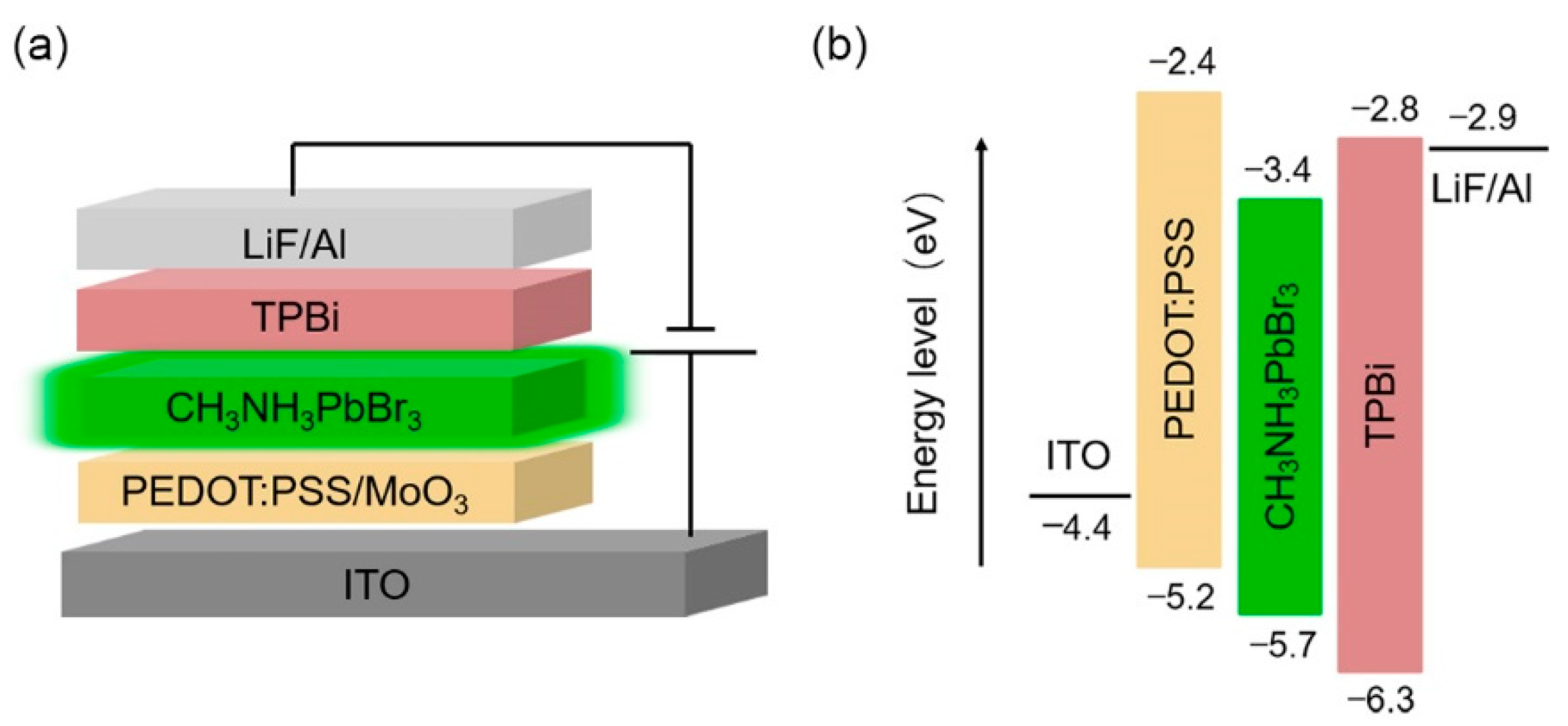
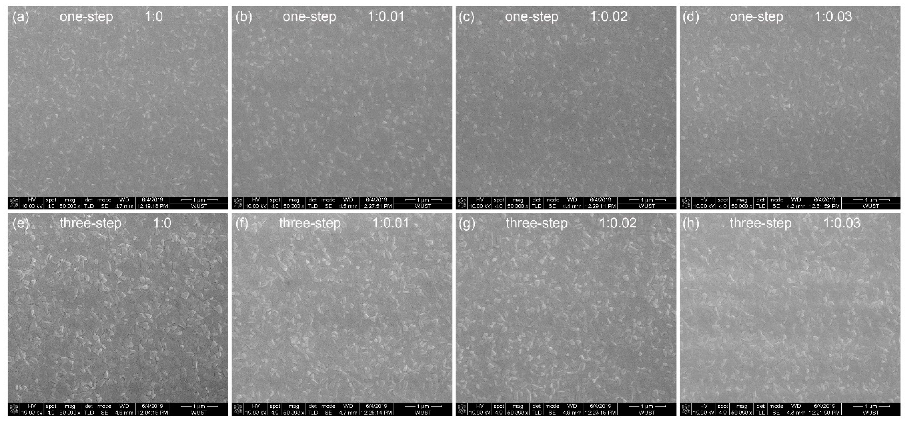
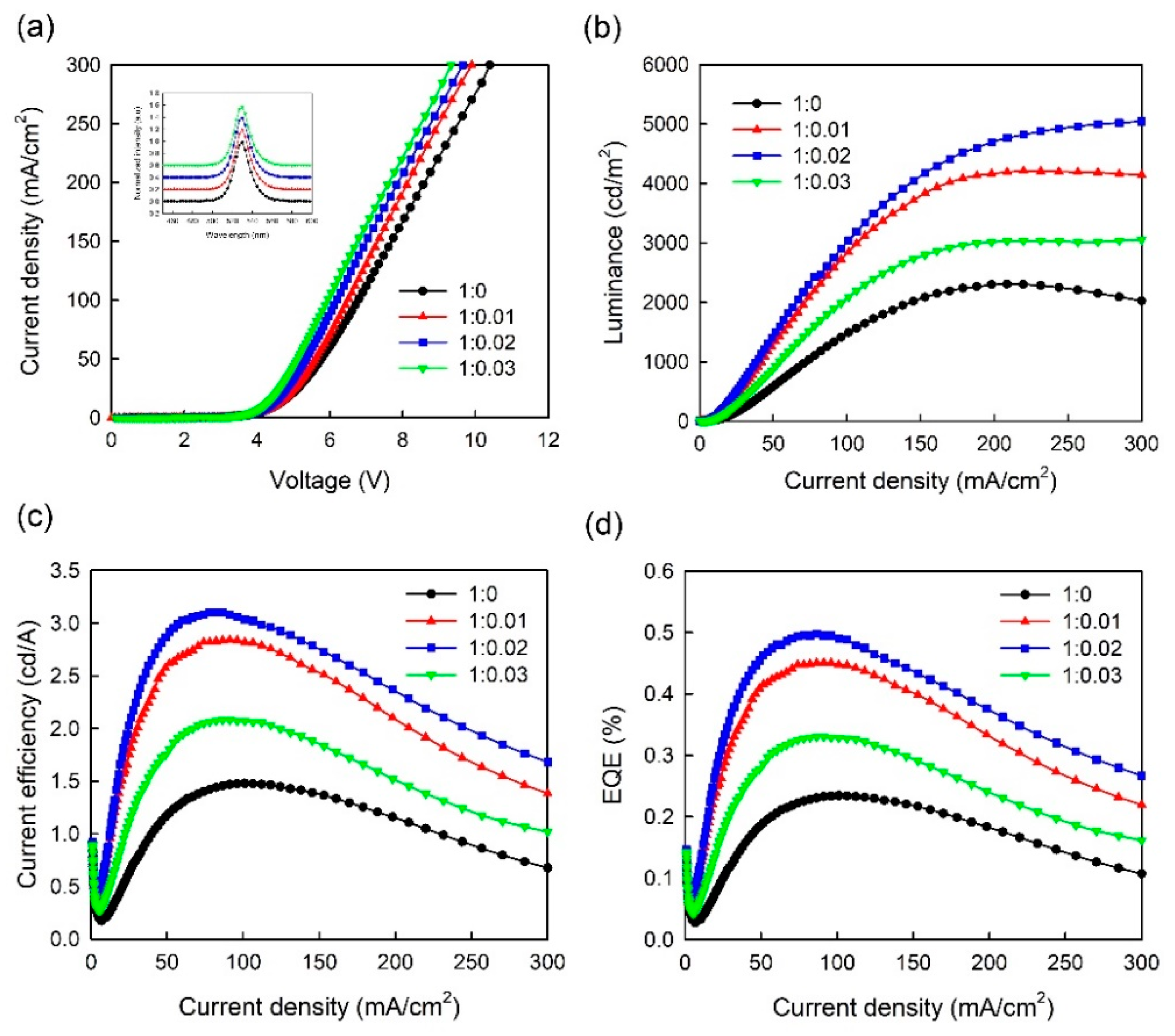
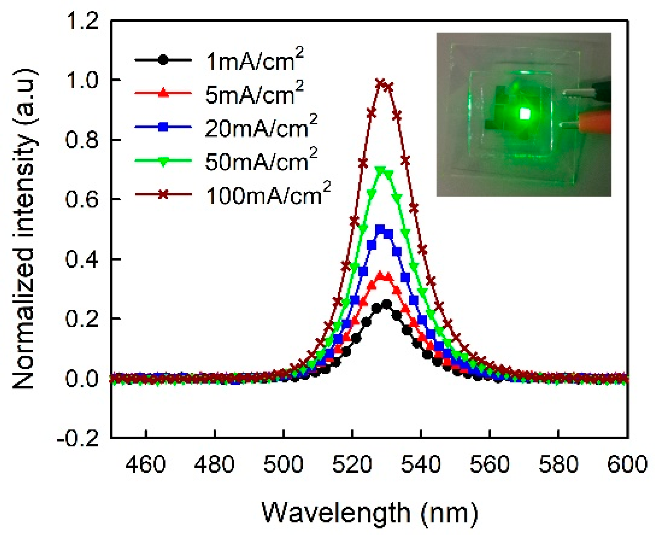
3. Results and Discussion

Figure 1a shows the schematic structure of our PeLEDs, which consist of ITO as a transparent anode, the PEDOT:PSS/MoO3-ammonia composite as a HTL, CH3NH3PbBr3 as an EML, TPBi as an ETL, LiF as an EIL, and Al as a cathode, respectively. To obtain good surface morphology of CH3NH3PbBr3 films, they were prepared by one-step and three-step spin coating of a CH3NH3PbBr3 precursor respectively. Figure 1b shows energy level diagrams of the PeLEDs with a pure PEDOT:PSS HTL. It is noted that the energy barrier between the PEDOT:PSS and CH3NH3PbBr3 layers is ~0.5 eV, which may result in low device efficiency. The doping of MoO3-ammonia in the PEDOT:PSS is expected to increase the work function of the PEDOT:PSS HTL and correspondingly reduce the contact barrier between the HTL and the CH3NH3PbBr3 EML for efficient hole injection [25,26].
Figure 2 shows the SEM images of CH3NH3PbBr3 films prepared on pure PEDOT:PSS and PEDOT:PSS/MoO3-ammonia composite HTLs [glass/ITO/composite HTL (~40 nm)/CH3NH3PbBr3 (~30 nm for one-step spin coating, ~55 nm for three-step spin coating)], respectively. The effect of the small MoO3-ammonia amount on the surface morphology of CH3NH3PbBr3 film is not evident. As reported in the literature, multi-step spin coating is expected to improve the surface morphology of perovskite film [27,28]. As shown in Figure 2, uniform and compact perovskite films with enhanced crystallinity formed on increasing the coating times from one to three.
Figure 3 shows XRD patterns of one-step and three-step coated CH3NH3PbBr3 films (glass/composite HTL (~40 nm)/CH3NH3PbBr3 (~30 nm for one-step spin coating, ~55 nm for three-step spin coating)). All the XRD patterns show two characteristic peaks at 15° and 30°, assigned to (100) and (200) crystal planes respectively, suggesting the crystal growth orientation along (100) planes. As shown in Figure 3a, the intensity of diffraction peaks was enhanced in three-step spin-coated CH3NH3PbBr3 film compared with one-step spin-coated CH3NH3PbBr3 film on pure PEDOT:PSS film, suggesting a better crystallization on increasing the coating time from one to three. As shown in Figure 3b, on increasing the ratio of MoO3-ammonia from 0 to 0.03, the intensity of diffraction peaks of three-step spin-coated CH3NH3PbBr3 film increases monotonically. The similar trend is also found in the one-step spin-coated CH3NH3PbBr3 films with different MoO3-ammonia ratios. This result is well consistent with previously reported results [25,26], which may be explained by that the MoO3 particles can act as crystal nuclei for the growth of spin-coated perovskite film.
Figure 4 shows steady-state PL spectra of one-step and three-step coated CH3NH3PbBr3 films [glass/ITO/composite HTL (~40 nm)/CH3NH3PbBr3 (~30 nm for one-step spin coating, ~55 nm for three-step spin coating)] conducted by using a luminescence spectrometer with an excitation wavelength of 315 nm. All the PL spectra show a well-defined peak at ~528 nm. As shown in Figure 4a, PL intensity was enhanced in three-step spin-coated CH3NH3PbBr3 film compared with one-step spin-coated CH3NH3PbBr3 film on pure PEDOT:PSS film. It can be explained by that the amount and morphology of perovskite material affect the PL intensity, namely more excitons will be generated by increasing the amount of perovskite particles, leading to the enhancement of the PL intensity when the thickness of perovskite film increases from ~30 nm (one-step coating) to ~55 nm (three-step coating) shown in Figure 4a. As shown in Figure 4b, on increasing the ratio of MoO3-ammonia from 0 to 0.02, the PL intensity of three-step spin-coated CH3NH3PbBr3 film gradually increases, while the further increase of the amount of MoO3-ammonia leads to the decrease of the PL intensity. The similar trend is also found in the one-step spin-coated CH3NH3PbBr3 films with different MoO3-ammonia ratios. It is suggested that the optimal MoO3-ammonia ratio is beneficial for blocking the exciton quenching at the HTL/CH3NH3PbBr3 interface, while the excessive MoO3-ammonia ratio is unfavorable. These results may be due to the increase of MoO3 on top of the HIL separating excitons generated in the CH3NH3PbBr3 EML from the quenching of PEDOT:PSS. However, on increasing the MoO3-ammonia amount, dopant aggregation or trap states may also occur at the HTL/EML interface, leading to the decay of photoluminescence. Figure 4c shows the transmittance spectra of PEDOT:PSS and PEDOT:PSS/MoO3-ammonia composite films with different MoO3-ammonia ratios (glass/ITO/composite HTL (~40 nm)). As shown in transmittance spectra, a small amount of MoO3 has little effect on the transmittance of PEDOT:PSS/MoO3-ammonia composite films in the visible range. The transmittances of four samples are near-identical, indicating that the doping of MoO3-ammonia in PEDOT:PSS HTL cannot impede the light passing through the HTL in this work. Figure 4d shows the absorption spectra of one-step and three-step spin-coated perovskite films on pure PEDOT:PSS HTL. Both two absorption spectra show a well-defined peak at ~526 nm. Furthermore, the absorption intensity was enhanced on increasing the coating time from one to three, which can be attributed to the increase of the thickness of perovskite film from ~30 nm (one-step coating) to ~55 nm (three-step coating).
Figure 5 shows (a) the current density vs. voltage (J-V), (b) the luminance vs. current density (L-J), (c) the current efficiency vs. current density (CE-J), and (d) the EQE vs. current density (EQE-J) curves for the single-step CH3NH3PbBr3 PeLEDs with pure PEDOT:PSS and PEDOT:PSS/MoO3-ammonia (1:0.01, 1:0.02, 1:0.03) composite HTLs. These four devices are labelled as S1, S2, S3, and S4 for clarity respectively. The detailed device parameters of the PeLEDs (S1, S2, S3, S4) are summarized in Table 1. As shown in Figure 5a, on increasing the MoO3-ammonia ratio from 0 to 0.03, the turn-on voltage, which are defined as the driving voltage at ∼1 mA/cm2, decreases monotonically from 4.3 V to 4.14 V. Besides, the current density of the PeLEDs increases on increasing the MoO3-ammonia amount, suggesting a reduced energy barrier at HTL/EML interface, inducing more efficient hole injection into CH3NH3PbBr3 layer [25,26]. As described in the L-J, CE-J, and EQE-J characteristics, a maximum luminance of 1082 cd/m2, a maximum CE of 0.7 cd/A and a maximum EQE of 0.11% were observed in the device with the MoO3-ammonia ratio of 0.02 (device S3), indicating the optimal volume ratio, while for the control device with pure PEDOT:PSS HTL (device S1), the maximum luminance of 593 cd/m2 and maximum CE of 0.36 cd/A were obtained. Therefore, the optimized device shows a 82% enhancement in the maximum luminance and 94% enhancement in the maximum CE respectively.
These results suggest that the hole injection in the PeLEDs with the PEDOT:PSS/MoO3-ammonia composite layer can be improved by reducing the contact barrier [25,26] and blocking the exciton quenching at the HTL/CH3NH3PbBr3 interface [26]. However, the device efficiency decreases when an excessive MoO3-ammonia amount was doped in the PEDOT:PSS/MoO3-ammonia composite HTL (0.03), possibly due to the trap states formed at HTL/EML interface after the doping of the excessive MoO3-ammonia. The inset in Figure 5a shows the normalized electroluminescence (EL) spectra of CH3NH3PbBr3 PeLEDs using PEDOT:PSS/MoO3-ammonia composite HTLs with different amounts of MoO3-ammonia, indicating that the EL spectra of PeLEDs with composite HTLs (S2, S3, S4) are nearly identical to that with pure PEDOT:PSS HTL (S1). It is suggested that the MoO3-ammonia doping cannot modify the emission profiles of CH3NH3PbBr3 PeLEDs, which have an EL peak at ∼528 nm.
Figure 6 shows J-V, L-J, CE-J, and EQE-J curves for the three-step CH3NH3PbBr3 PeLEDs with pure PEDOT:PSS and PEDOT:PSS/MoO3-ammonia (1:0.01, 1:0.02, 1:0.03) composite HTLs, which are labelled as T1, T2, T3, and T4 for clarity respectively. The detailed device parameters of the PeLEDs (T1, T2, T3, T4) are summarized in Table 2. As shown in Figure 6a, on increasing the MoO3-ammonia ratio from 0 to 0.03, the turn-on voltage decreases from 4.08 V to 3.68 V. Besides, the current density of the PeLEDs increases on increasing the MoO3-ammonia amount, which is similar to the trend observed in one-step devices (S1, S2, S3, S4). As shown in Figure 6c,d, the CE and EQE increase at low current densities because of the rapidly increased luminance (or the number of excitons). On further increasing the current density, the luminance increases more slowly or decreases, leading to the decreased CE and EQE, namely the efficiency roll-off. As reported, the efficiency roll-off of OLEDs is mainly caused by charge imbalance and quenching processes [10,29,30]. Similarly, in this work, higher CE found in the device with the MoO3-ammonia ratio of 0.02 can be explained by the balance of electrons and holes in the EM, as well as the reduced exciton quenching. From the L-J, CE-J, and EQE-J characteristics, a maximum luminance of 5044 cd/m2, a maximum CE of 3.12 cd/A and a maximum EQE of 0.5% were also observed in the device with the optimal MoO3-ammonia ratio of 0.02 (device T3), while for the device with pure PEDOT:PSS HTL (device T1), the maximum luminance of 2309 cd/m2 and maximum CE of 1.47 cd/A were obtained. Thus, the optimized device shows a 118% enhancement in the maximum luminance and 112% enhancement in the maximum CE respectively. Compared with the control device with pure PEDOT:PSS HTL and one-step spin-coated CH3NH3PbBr3 film (device S1), a 750% enhancement in the maximum luminance and 767% enhancement in the maximum CE were obtained for the optimized device (device T3). The inset in Figure 6a shows the normalized EL spectra of three-step CH3NH3PbBr3 PeLEDs using PEDOT:PSS/MoO3-ammonia composite HTLs with different amounts of MoO3-ammonia, in which all PeLEDs have an EL peak at ∼528 nm. Figure 7 shows the EL curves measured at different current densities. The results indicate that all PeLEDs have an EL peak at ~528 nm, suggesting the color stability of our devices.
These results indicate that the hole injection in the PeLEDs with the PEDOT:PSS/MoO3-ammonia composite layer can be improved by reducing the contact barrier [25,26] and suppressing the exciton quenching at the HTL/CH3NH3PbBr3 interface [26]. Besides, three-step spin coating method can improve the surface morphology of the CH3NH3PbBr3 perovskite film shown in Figure 2. Furthermore, the as-obtained perovskite layer exhibited a stronger PL intensity shown in Figure 4. These factors induce the significant improvement on luminous performance of our PeLEDs. Therefore, the significantly improved efficiency of PeLEDs using three-step spin-coated CH3NH3PbBr3 film and an optimum PEDOT:PSS/MoO3-ammonia composite HTL can be explained by the enhanced carrier recombination through better hole injection and film morphology optimization, as well as the reduced exciton quenching at HTL/CH3NH3PbBr3 interface.

4. Conclusions

In summary, we demonstrated improved performance of PeLEDs using a PEDOT:PSS/MoO3-ammonia composite HTL by reducing the energy barrier and blocking the exciton quenching at the HTL/CH3NH3PbBr3 interface. For PeLEDs with one-step spin-coated CH3NH3PbBr3 film, an enhancement of 82% in the maximum luminance and 94% in the maximum CE was found in PeLED with an optimal MoO3-ammonia volume ratio (0.02) in PEDOT:PSS/MoO3-ammonia composite HTL compared with the control device with pure PEDOT:PSS HTL respectively. Three-step spin coating method was further used to obtain uniform and dense CH3NH3PbBr3 films, which lead to a maximum luminance of 5044 cd/m2 and maximum CE of 3.12 cd/A, which are 750% and 767% larger than those of the control device respectively. The significantly improved efficiency of PeLEDs using three-step spin-coated CH3NH3PbBr3 film and an optimum PEDOT:PSS/MoO3-ammonia composite HTL can be originated from the enhanced carrier recombination through better hole injection and film morphology optimization, as well as the reduced exciton quenching at HTL/CH3NH3PbBr3 interface. These results suggest a promising clue for the device engineering of high efficiency PeLEDs.

Author Contributions

Conceptualization, Y.Z. and F.M.; Funding acquisition, Y.Z. and F.M.; Investigation, S.M., D.S. and N.L.; Methodology, S.M., W.S., J.F., J.X., Y.J. and X.C.; Writing—original draft, S.M.; Writing—review & editing, Y.Z.

Funding

This work was supported by the Foundation of Hubei Provincial Science and Technology Department (Grant No. 2016BKJ005), the Leading Plan of Green Industry of Hubei University of Technology (Grant No. YXQN2016003), the International Science and Technology Cooperation Program of China (Grant No. 2016YFE0124300), the Open Foundation of Hubei Key Laboratory for High-efficiency Use of Solar Energy and Operation Control of Energy Storage System (Grant Nos. HBSEES201801, HBSEES201705), and the National Natural Science Foundation of China (Grant Nos. 51602099, 51371079, 11304092, and 11305056).

Acknowledgments

We thank Lixia Fan in Wuhan University of Science and Technology for technical assistance.

Conflicts of Interest

The authors declare no conflict of interest.

References

  1. Era, M.; Morimoto, S.; Tsutsui, T.; Saito, S. Organic-inorganic heterostructure electroluminescent device using a layered perovskite semiconductor (C6H5C2H4NH3)2PbI4. Appl. Phys. Lett. 1994, 65, 676. [Google Scholar] [CrossRef]
  2. Koutselas, I.; Bampoulis, P.; Maratou, E.; Evagelinou, T.; Pagona, G.; Papavassiliou, G.C. Some unconventional organic−inorganic hybrid low-dimensional semiconductors and related light-emitting devices. J. Phys. Chem. C 2011, 115, 8475–8483. [Google Scholar] [CrossRef]
  3. Tan, Z.K.; Moghaddam, R.S.; Lai, M.L.; Docampo, P.; Higler, R.; Deschler, F.; Price, M.; Sadhanala, A.; Pazos, L.M.; Credgington, D.; et al. Bright light-emitting diodes based on organometal halide perovskite. Nat. Nanotechnol. 2014, 9, 687–692. [Google Scholar] [CrossRef] [PubMed]
  4. Cho, H.C.; Jeong, S.H.; Park, M.H.; Kim, Y.H.; Wolf, C.; Lee, C.L.; Heo, J.H.; Sadhanala, A.; Myoung, N.; Yoo, S.; et al. Overcoming the electroluminescence efficiency limitations of perovskite light-emitting diodes. Science 2015, 350, 1222–1225. [Google Scholar] [CrossRef] [PubMed]
  5. Kim, Y.H.; Cho, H.; Heo, J.H.; Kim, T.S.; Myoung, N.; Lee, C.L.; Im, S.H.; Lee, T.W. Multicolored organic/inorganic hybrid perovskite light-emitting diodes. Adv. Mater. 2015, 27, 1248–1254. [Google Scholar] [CrossRef] [PubMed]
  6. Lin, K.B.; Xing, J.; Quan, L.N.; de Arquer, F.P.G.; Gong, X.W.; Lu, J.X.; Xie, L.Q.; Zhao, W.J.; Zhang, D.; Yan, C.Z.; et al. Perovskite light-emitting diodes with external quantum efficiency exceeding 20 per cent. Nature 2018, 562, 245–248. [Google Scholar] [CrossRef] [PubMed]
  7. Cao, Y.; Wang, N.N.; Tian, H.; Guo, J.S.; Wei, Y.Q.; Chen, H.; Miao, Y.F.; Zou, W.; Pan, K.; He, Y.R.; et al. Perovskite light-emitting diodes based on spontaneously formed submicrometre-scale structures. Nature 2018, 562, 249–253. [Google Scholar] [CrossRef]
  8. Kim, Y.H.; Lee, S.H.; Noh, J.; Han, S.H. Performance and stability of electroluminescent device with self-assembled layers of poly(3,4-ethylenedioxythiophene)-poly(styrenesulfonate) and polyelectrolytes. Thin Solid Films 2006, 510, 305–310. [Google Scholar] [CrossRef]
  9. Kim, J.S.; Friend, R.H.; Grizzi, I.; Burroughes, J.H. Spin-cast thin semiconducting polymer interlayer for improving device efficiency of polymer light-emitting diodes. Appl. Phys. Lett. 2005, 87, 023506. [Google Scholar] [CrossRef]
  10. Liu, N.; Mei, S.J.; Sun, D.W.; Shi, W.X.; Feng, J.H.; Zhou, Y.M.; Mei, F.; Xu, J.X.; Jiang, Y.; Cao, X.A. Effects of charge transport materials on blue fluorescent organic light-emitting diodes with a host-dopant system. Micromachines 2019, 10, 344. [Google Scholar] [CrossRef]
  11. You, H.; Dai, Y.F.; Zhang, Z.Q.; Ma, D.G. Improved performances of organic light-emitting diodes with metal oxide as anode buffer. J. Appl. Phys. 2007, 101, 026105. [Google Scholar] [CrossRef]
  12. Li, J.Z.; Yahiro, M.; Ishida, K.; Yamada, H.; Matsushige, K. Enhanced performance of organic light emitting device by insertion of conducting/insulating WO3 anodic buffer layer. Synth. Met. 2005, 151, 141. [Google Scholar] [CrossRef]
  13. Meyer, J.; Zilberberg, K.; Riedl, T.; Kahn, A. Electronic structure of Vanadium pentoxide: An efficient hole injector for organic electronic materials. J. Appl. Phys. 2011, 110, 033710. [Google Scholar] [CrossRef]
  14. Shrotriya, V.; Li, G.; Yao, Y.; Chu, C.W.; Yang, Y. Transition metal oxides as the buffer layer for polymer photovoltaic cells. Appl. Phys. Lett. 2006, 88, 073508. [Google Scholar] [CrossRef] [Green Version]
  15. Shi, W.X.; Liu, N.; Zhou, Y.M.; Cao, X.A. Effects of postannealing on the characteristics and reliability of polyfluorene organic light-emitting diodes. IEEE Trans. Electron Devices 2019, 66, 1057–1062. [Google Scholar] [CrossRef]
  16. Zhao, Y.B.; Chen, J.S.; Chen, W.; Ma, D.G. Poly(3,4-ethylenedioxythiophene): Poly(styrenesulfonate)/MoO3 composite layer for efficient and stable hole injection in organic semiconductors. J. Appl. Phys. 2012, 111, 043716. [Google Scholar] [CrossRef]
  17. Meyer, J.; Khalandovsky, R.; Gorrn, P.; Kahn, A. MoO3 films spin-coated from a nanoparticle suspension for efficient hole-injection in organic electronics. Adv. Mater. 2011, 23, 70–73. [Google Scholar] [CrossRef]
  18. Wong, K.H.; Ananthanarayanan, K.; Luther, J.; Balaya, P. Origin of hole selectivity and the role of defects in low-temperature solution-processed molybdenum oxide interfacial layer for organic solar cells. J. Phys. Chem. C 2012, 116, 16346–16351. [Google Scholar] [CrossRef]
  19. Murase, S.; Yang, Y. Solution processed MoO3 interfacial layer for organic photovoltaics prepared by a facile synthesis method. Adv. Mater. 2012, 24, 2459–2462. [Google Scholar] [CrossRef]
  20. Sun, J.Y.; Tseng, W.H.; Lan, S.; Lin, S.H.; Yang, P.C.; Wu, C.I.; Lin, C.F. Performance enhancement in inverted polymer photovoltaics with solution-processed MoOx and air-plasma treatment for anode modification. Sol. Energy Mater. Sol. Cells 2013, 109, 178–184. [Google Scholar] [CrossRef]
  21. Liu, F.M.; Shao, S.Y.; Guo, X.Y.; Zhao, Y.; Xie, Z.Y. Efficient polymer photovoltaic cells using solution-processed MoO3 as anode buffer layer. Sol. Energy Mater. Sol. Cells 2010, 94, 842–845. [Google Scholar] [CrossRef]
  22. Hou, F.H.; Su, Z.S.; Jin, F.M.; Yan, X.W.; Wang, L.D.; Zhao, H.F.; Zhu, J.Z.; Chu, B.; Li, W.L. Efficient and stable planar heterojunction perovskite solar cells with an MoO3/PEDOT:PSS hole transporting layer. Nanoscale 2015, 7, 9427–9432. [Google Scholar] [CrossRef] [PubMed]
  23. Sung, H.; Ahn, N.; Jang, M.S.; Lee, J.K.; Yoon, H.; Park, N.G.; Choi, M. Transparent Conductive Oxide-Free Graphene-Based Perovskite Solar Cells with over 17% Efficiency. Adv. Energy Mater. 2016, 6, 1501873. [Google Scholar] [CrossRef]
  24. Zheng, Q.H.; Li, W.S.; Zhang, Y.; Xu, K.; Xu, J.W.; Wang, H.; Xiong, J.; Zhang, X.Y.; Zhang, X.W. Solution-processed composite interfacial layer of MoOx-doped graphene oxide for robust hole injection in organic light-emitting diode. Phys. Status Solidi RRL 2018, 12, 1700434. [Google Scholar] [CrossRef]
  25. Kim, D.B.; Yu, J.C.; Nam, Y.S.; Kim, D.W.; Jung, E.D.; Lee, S.Y.; Lee, S.; Park, J.H.; Lee, A.Y.; Lee, B.R.; et al. Improved performance of perovskite light-emitting diodes using a PEDOT:PSS and MoO3 composite layer. J. Mater. Chem. C 2016, 4, 8161–8165. [Google Scholar] [CrossRef]
  26. Meng, Y.; Ahmadi, M.; Wu, X.Y.; Xu, T.F.; Xu, L.; Xiong, Z.H.; Chen, P. High performance and stable all-inorganic perovskite light emitting diodes by reducing luminescence quenching at PEDOT:PSS/perovskites interface. Org. Electron. 2019, 64, 47–53. [Google Scholar] [CrossRef]
  27. Feng, Z.Q.; Wang, L.; Yu, H.T.; Ma, X.Q.; Zhang, Q.; Chen, S.F.; Liu, L.H.; Huang, W. Towards efficient perovskite light-emitting diodes: A multi-step spin-coating method for a dense and uniform perovskite film. Org. Electron. 2018, 61, 18–24. [Google Scholar] [CrossRef]
  28. Qasim, K.; Wang, B.P.; Zhang, Y.P.; Li, P.F.; Wang, Y.S.; Li, S.J.; Lee, S.T.; Liao, L.S.; Lei, W.; Bao, Q.L. Solution-processed extremely efficient multicolor perovskite light-emitting diodes utilizing doped electron transport layer. Adv. Funct. Mater. 2017, 27, 1606874. [Google Scholar] [CrossRef]
  29. Giebink, N.C.; Forrest, S.R. Quantum efficiency roll-off at high brightness in fluorescent and phosphorescent organic light emitting diodes. Phys. Rev. B 2008, 77, 235215. [Google Scholar] [CrossRef]
  30. Murawski, C.; Leo, K.; Gather, M.C. Efficiency roll-off in organic light-emitting diodes. Adv. Mater. 2013, 25, 6801–6827. [Google Scholar] [CrossRef]
Figure 1. (a) The schematic structure of our PeLEDs. (b) The energy level diagram of the PeLEDs with a pure PEDOT:PSS HTL.
Micromachines 10 00459 g001
Figure 2. SEM images of the one-step spin-coated CH3NH3PbBr3 film samples on (a) PEDOT:PSS, (b) PEDOT:PSS/MoO3-ammonia (1:0.01), (c) PEDOT:PSS/MoO3-ammonia (1:0.02), (d) PEDOT:PSS/MoO3-ammonia (1:0.03) composite HTLs, and three-step spin-coated CH3NH3PbBr3 film samples on (e) PEDOT:PSS, (f) PEDOT:PSS/MoO3-ammonia (1:0.01), (g) PEDOT:PSS/MoO3-ammonia (1:0.02), (h) PEDOT:PSS/MoO3-ammonia (1:0.03) composite HTLs.
Micromachines 10 00459 g002
Figure 3. XRD patterns of (a) one-step and three-step coated CH3NH3PbBr3 films on the pure PEDOT:PSS film, (b) three-step coated CH3NH3PbBr3 films on the pure PEDOT:PSS film and PEDOT:PSS/MoO3-ammonia composite HTLs with different MoO3 ratios. The XRD patters were shifted vertically for clarity.
Micromachines 10 00459 g003
Figure 4. PL spectra of (a) one-step and three-step coated CH3NH3PbBr3 films on the pure PEDOT:PSS film, (b) three-step coated CH3NH3PbBr3 films on the pure PEDOT:PSS film and PEDOT:PSS/MoO3-ammonia composite HTLs with different MoO3-ammonia ratios. (c) The transmittance spectra of the pure PEDOT:PSS film and PEDOT:PSS/MoO3-ammonia composite HTLs with different MoO3-ammonia ratios. (d) The absorption spectra of one-step and three-step spin-coated perovskite films on pure PEDOT:PSS HTL.
Micromachines 10 00459 g004
Figure 5. (a) J-V, (b) L-J, (c) CE-J, (d) EQE-J curves of PeLEDs with a one-step spin-coated emitter and a PEDOT:PSS/MoO3-ammonia (1:0, 1:0.01, 1:0.02, 1:0.03) composite HTL (device S1, S2, S3, S4). The inset is normalized EL spectra of the PeLED devices at 20 mA/cm2, which were shifted vertically for clarity.
Micromachines 10 00459 g005
Figure 6. (a) J-V, (b) L-J, (c) CE-J, (d) EQE-J curves of PeLEDs with a three-step spin-coated emitter and a PEDOT:PSS/MoO3-ammonia (1:0, 1:0.01, 1:0.02, 1:0.03) composite HTL (device T1, T2, T3, T4). The inset is normalized EL spectra of the PeLED devices at 20 mA/cm2, which were shifted vertically for clarity.
Micromachines 10 00459 g006
Figure 7. EL spectra of the PeLED devices with a three-step spin-coated emitter and a PEDOT:PSS/MoO3-ammonia (1:0.02) composite HTL at different current densities. The inset is a luminescence image of the device at 50 mA/cm2.
Micromachines 10 00459 g007
Table 1. Summary of the device parameters of PeLEDs (device S1, S2, S3, S4) with a single-step spin-coated emitter and a PEDOT:PSS/MoO3-ammonia (1:0, 1:0.01, 1:0,02, 1:0.03) composite HTL.
Volume Ratio of PEDOT:PSS/MoO3-AmmoniaLmax (cd/m2)CEmax (cd/A)EQEmax (%)Turn-on Voltage (V)
1:0 (S1)5930.360.0574.3
1:0.01 (S2)8160.50.0794.22
1:0.02 (S3)10820.70.114.18
1:0.03 (S4)6240.420.0684.14
Table 2. Summary of the device parameters of PeLEDs (device T1, T2, T3, T4) with a three-step spin-coated emitter and a PEDOT:PSS/MoO3-ammonia (1:0, 1:0.01, 1:0,02, 1:0.03) composite HTL.
Volume Ratio of PEDOT:PSS/MoO3-AmmoniaLmax (cd/m2)CEmax (cd/A)EQEmax (%)Turn-on Voltage (V)
1:0 (T1)23091.470.234.08
1:0.01 (T2)42152.840.453.84
1:0.02 (T3)50443.120.53.75
1:0.03 (T4)30552.080.333.68

