Investigation of Plasma Activated Si-Si Bonded Interface by Infrared Image Based on Combination of Spatial Domain and Morphology


Abstract
1. Introduction
2. Experimental Methods
2.1. Materials and Bonding Process
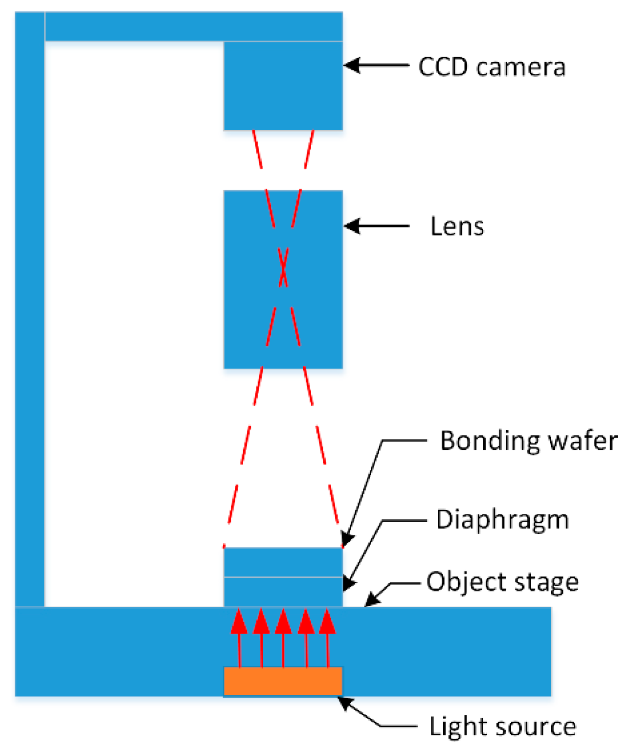
2.2. Infrared Imaging System
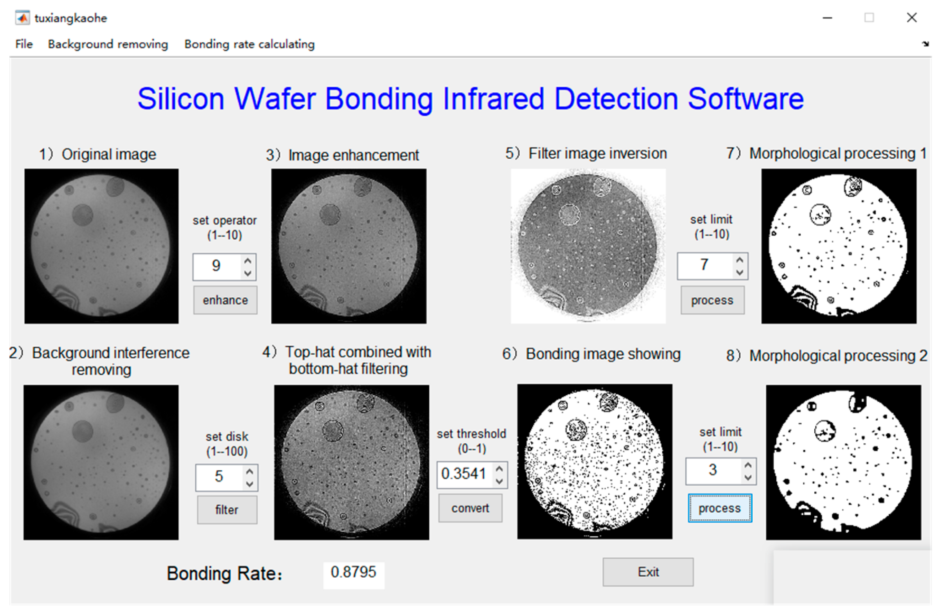
- Load an infrared image. A square image is needed, which means that the number of pixel rows in the image must be equal with the number of pixel columns because a square matrix is required to convolve with the sharpened operator during the image enhancement process.
- Background interference removing by using median filter in the spatial domain, which also called image denoising. As we know, the image acquired by CCD camera is severely affected by discrete impulse noise and salt-pepper noise. These kinds of noises are commonly derived from the electronic circuit and sensor caused by low illumination or high temperature, and can be effectively removed by median filter method. Suppose that denotes the gray value of each point of the digital image, and the two-dimensional median filtering window A can be defined asIt is a nonlinear smoothing filtering method that removes noise while preserving the sharpness and detail of the image. By this way, most of the noise mixed in the digitized image is eliminated, which lays a good foundation for the subsequent detail information extraction.
- Image enhancement by Laplacian operator. The Laplacian operator is suitable for refining the image blur caused by diffuse reflection of light. It is an isotropic second-order differential operator. For a continuous binary function , the Laplacian at position is delineated asThe sharpening filter in the spatial domain can be expressed in convolution form aswhere is the sharpening operator pattern. The edges and contours of the image are generally located at the position where the grayscale is abrupt, that is, the high frequency part of the image. The edges are usually extracted by the grayscale difference, which is often in any directions. So the differential operations need to be directional. The isotropic edge detection operator has the same detection capability for edge contours regardless of their directions. The method is to achieve image enhancement through two normalized high-pass filter patterns, which weakens or removes the low-frequency part of the image, meanwhile retains the high-frequency part of the image. Their equations are shown as below:The normalization method is to subtract the Laplacian operator from the original image, H1 is a four-neighbor pattern, H2 is an eight-neighbor pattern, and the discrete function expressions are respectively:This method appertains to a sort of linear sharpening filtering, which can avoid the brightness deviation of the processed image, and may restore the background data while ensuring the Laplacian sharpening effect, so that highlight the edge information well.
- Make use of the combination of Top-Hat and Bottom-Hat filtering method to enhance the contrast. Firstly, the enhanced image is added to the Top-Hat filtered image, and then the Bottom-Hat filtered image is subtracted. Finally, the filtered image is inverted to achieve the negative film effect. In this part, a value, called disk size, is set to adjust the influence of the contrast strength. The disk size ranges from 1 to 100. In addition, it is also possible to suppress mixed noise composed by Gaussian noise and impulse noise in the infrared image. This method makes the outer boundary of the bonded wafers more obvious, and the texture of the interference fringe is more prominent.
- Invert the filtered image to achieve the negative effect. In general, uint8 represents 256-level grayscale in the image file, and the range of data is 0~255. The negative effect of the image is to subtract the original image data by 255. It is convenient to analyze the filtering situation compared with the image in the previous step.
- Set the binarization threshold to display the bonding area. This is the vital step for a better result. A large number of image tests show that the extent of threshold is regularly between 0.2 and 0.5. It is requested to conserve the complete information of the image without introducing excessive noise pixels.
- Properly perform the morphological processing. The purpose of the first morphological processing is to extract the main body. It requests the effective pixel points that are not bonded and filters out the imported noise pixel points after binarization. To obtain the information as complete as possible of each part of the image in the end. Need to pay attention that the processing times are Inf until the image no longer changes. The reason why the mode can be modified aims to find out how many times it takes to reach a steady state, mostly covering from 1 to 10.
- Fill the holes and achieve the bonding region connectivity by several erosion and dilation. In the field of image processing, connectivity means the continuous and adjacent of pixels. There are several cases that will happen when a hole is filled. In the first case, the size of the holes is relatively uniform, and can be fully filled though multiple erosion and dilation. In the second case, the size of the holes is quite different. After the small holes are filled, the large holes are incompletely filled. Furthermore, the large and unfilled holes can be seen that either the outer boundary is closed, meaning the pixels of hole contour are continuous and adjacent, or some values are only left on the boundary, meaning the pixels of hole contour are fragmentary. The number of processing times is as less as possible and the range is primarily between 1 and 10.
- Calculate the bonding rate. For the first case above, the parameter is directly gained for calculation. While, the second case demands to invoke the circle fitting function to measure the area of all the holes, including the unsuccessful filled holes. The area refers to the sum of the pixel points. Afterwards, the parameter is secured to calculate the bonding rate.
2.3. Orthogonal Experiment Design
3. Software Evaluation
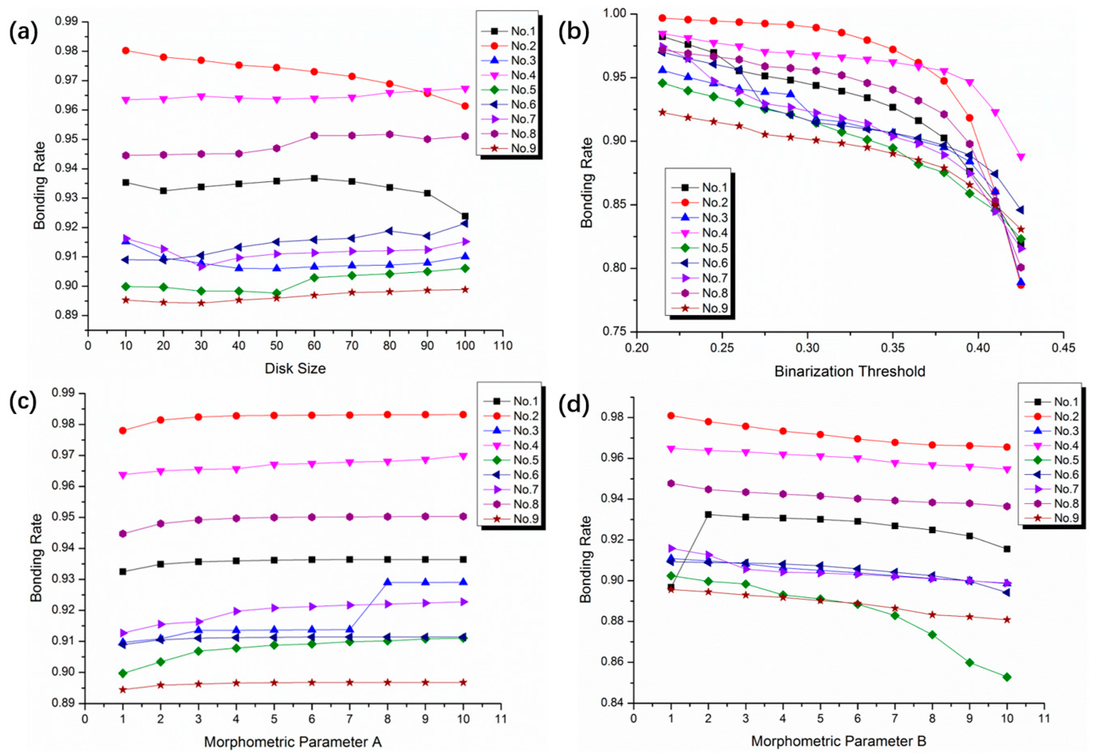
3.1. Four-Neighbor and Eight-Neighbor Sharpening Operator Patterns
3.2. Disk Size and Binarization Threshold
3.3. Morphological Parameter A and B
4. Void Formation and Characteristics
5. Orthogonal Experiment Analysis
6. Conclusions
- (1)
- Comparing the effects of four-neighbor and eight-neighbor sharpening operator pattern, it is well known that more salt and pepper noise will be imported using the eight-neighbor patter. After the first morphological processing, although most of the noise could be filtered out, the retention effect on the original information was worse than that of the four-neighbor pattern. As a result, the four-neighbor pattern was used for image enhancement processing in subsequent experiments.
- (2)
- Among the four parameters of disk size, binarization threshold, morphological parameter A and morphological parameter B, the binarization threshold had the most significant effect on the result, and the variation range of result was primarily maintained at 2%~5%. The other parameters all had an effect on the results within 2%. In addition, while processing images, it was also necessary to pay attention to the holes of individual features to bring about the effect of jump.
- (3)
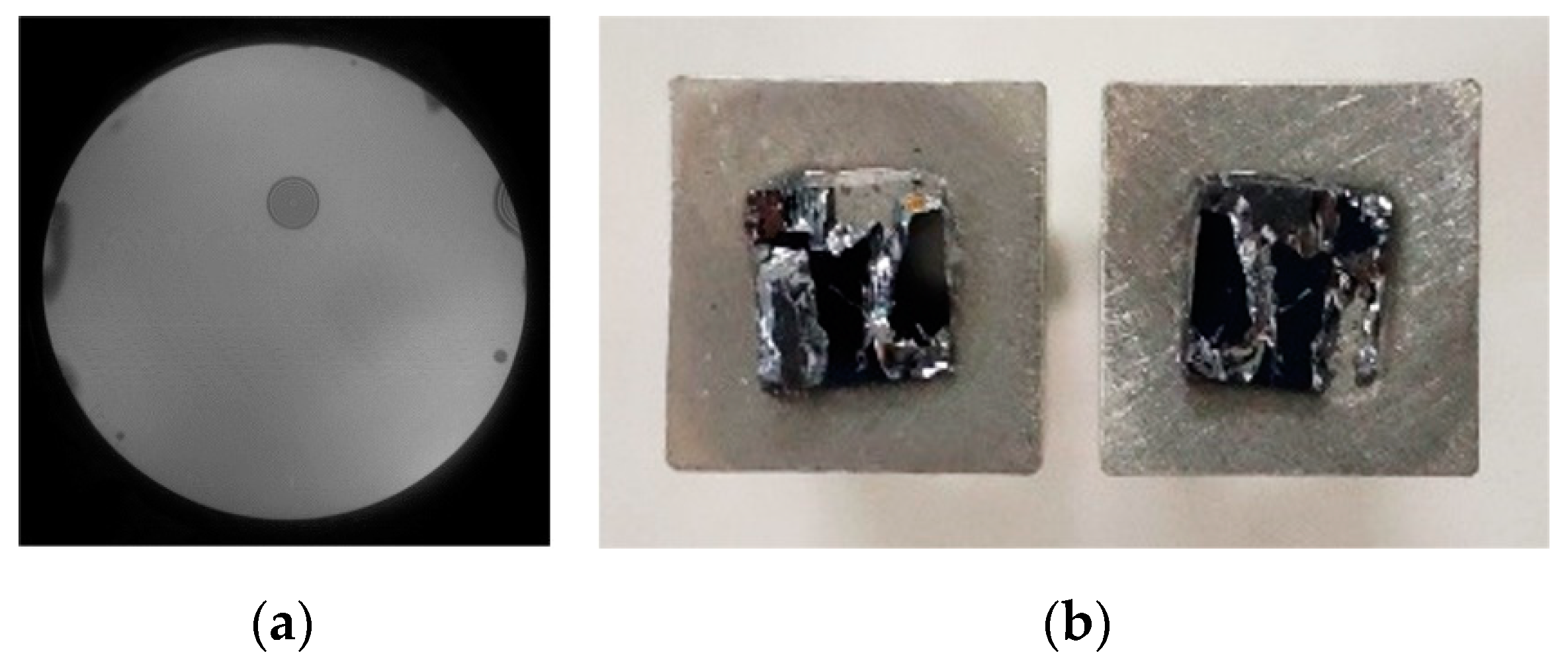
- The number of voids in the bonding interface can identify the bonding quality, while the diameter can infer the cause of void formation. For the unclear outline of voids (with <1 mm in diameters) caused by the byproduct H2 formed by the condensation reaction between Si-OH, they cannot be captured during software processing. Whereas, the final bonding result has only a one in ten thousand effect. The voids with a diameter ranging from 2 to 14 mm caused by the aggregation of water molecules and small particles can be easily acquired and completely removed via software processing, ensuring the accuracy of the results. Caused by large dust or organic contaminants, the voids were successfully divided and the connected domain was gained between 14 and 22 mm in diameter, which had a serious impact on the bonding rate.
- (4)
- The orthogonal experimental data show that the O2 flow has the greatest influence on bonding rate in comparison with activated time and power. The subsequent experiments particularly focused on the parameter selection of O2 flow. With the optimized process parameters of activated power of 150 W, O2 flow of 100 sccm, and time of 120 s, the bonding rate reached 94.51% and the bonding strength was 12.32 MPa.
Author Contributions
Funding
Conflicts of Interest
References
- Ryckeboer, E.; Gassenq, A.; Hattasan, N.; Kuyken, B.; Cerutti, L.; Rodriguez, J.B.; Tournie, E.; Roelkens, G.; Bogaerts, W.; Baets, R. Integrated spectrometer and integrated detectors on Silicon-on-Insulator for short-wave infrared applications. In Proceedings of the 2012 Conference on Lasers and Electro-Optics, San Jose, CA, USA, 6–11 May 2012. [Google Scholar]
- Keyvaninia, S.; Muneeb, M.; Stankovic, S.; Van Veldhoven, P.J.; Van Thourhout, D.; Roelkens, G. Ultra-thin DVS-BCB adhesive bonding of III-V wafers, dies and multiple dies to a patterned silicon-on-insulator substrate. Opt. Mater. Express 2013, 3, 35–46. [Google Scholar] [CrossRef]
- Yokoyama, M.; Yokoyama, H.; Takenaka, M.; Takagi, S. InGaSb-on-insulator p-channel metal-oxide-semiconductor field-effect transistors on Si fabricated by direct wafer bonding. J. Appl. Phys. 2019, 125, 114501. [Google Scholar] [CrossRef]
- Higurashi, E.; Okumura, K.; Nakasuji, K.; Suga, T. Surface activated bonding of GaAs and SiC wafers at room temperature for improved heat dissipation in high-power semiconductor lasers. Jpn. J. Appl. Phys. 2015, 54, 030207. [Google Scholar] [CrossRef]
- Dimroth, F.; Tibbits, T.N.D.; Niemeyer, M.; Predan, F.; Beutel, P.; Karcher, C.; Oliva, E.; Siefer, G.; Lackner, D.; Fuss-Kailuweit, P.; et al. Four-junction wafer-bonded concentrator solar cells. IEEE J. Photovolt. 2016, 6, 343–349. [Google Scholar] [CrossRef]
- Snyder, B.W.; O’Brien, P.A. Developments in packaging and integration for silicon photonics. In Reliability, Packaging, Testing, and Characterization of Moems/Mems and Nanodevices Xii; Ramesham, R., Shea, H.R., Eds.; SPIE: San Francisco, CA, USA, 2013; Volume 8614. [Google Scholar]
- Zoschke, K.; Manier, C.A.; Wilke, M.; Jurgensen, N. Hermetic wafer level packaging of MEMS components using through silicon via and wafer to wafer bonding technologies. In Proceedings of the Electronic Components & Technology Conference, Las Vegas, NV, USA, 28–31 May 2013. [Google Scholar]
- Zhang, L.; Liu, Z.Q.; Chen, S.W.; Wang, Y.D.; Long, W.M.; Guo, Y.H.; Wang, S.Q.; Ye, G.; Liu, W.Y. Materials, processing and reliability of low temperature bonding in 3D chip stacking. J. Alloy. Compd. 2018, 750, 980–995. [Google Scholar] [CrossRef]
- Wang, Z. 3-D integration and through-silicon vias in MEMS and microsensors. J. Microelectromech. Syst. 2015, 24, 1211–1244. [Google Scholar] [CrossRef]
- Higurashi, E.; Sasaki, Y.; Kurayama, R.; Suga, T.; Doi, Y.; Sawayama, Y.; Hosako, I. Room-temperature direct bonding of germanium wafers by surface-activated bonding method. Jpn. J. Appl. Phys. 2015, 54, 030213. [Google Scholar] [CrossRef]
- Howlader, M.M.R.; Zhang, F.; Kim, M.J. Annealing temperature-dependent interfacial behavior of sequentially plasma-activated silicon bonded wafers. J. Microelectromech. Syst. 2011, 20, 17–20. [Google Scholar] [CrossRef]
- Wang, C.X.; Suga, T. Investigation of fluorine containing plasma activation for room-temperature bonding of Si-based materials. Microelectron. Reliab. 2012, 52, 347–351. [Google Scholar] [CrossRef]
- Wang, C.; Wang, Y.; Tian, Y.; Wang, C.; Suga, T. Room-temperature direct bonding of silicon and quartz glass wafers. Appl. Phys. Lett. 2017, 110, 221602. [Google Scholar] [CrossRef]
- Fukushima, T.; Hashiguchi, H.; Yonekura, H.; Kino, H.; Murugesan, M.; Bea, J.-C.; Lee, K.-W.; Tanaka, T.; Koyanagi, M. Oxide-oxide thermocompression direct bonding technologies with capillary self-assembly for multichip-to-wafer heterogeneous 3D system integration. Micromachines 2016, 7, 184. [Google Scholar] [CrossRef]
- He, R.; Yamauchi, A.; Suga, T. Sequential plasma activation methods for hydrophilic direct bonding at sub-200 °C. Jpn. J. Appl. Phys. 2018, 57, 6. [Google Scholar] [CrossRef]
- Xu, J.; Wang, C.; Wang, T.; Wang, Y.; Kang, Q.; Liu, Y.; Tian, Y. Mechanisms for low-temperature direct bonding of Si/Si and quartz/quartz via VUV/O3 activation. RSC Adv. 2018, 8, 11528–11535. [Google Scholar] [CrossRef]
- Takigawa, R.; Higurashi, E.; Asano, T. Room-temperature wafer bonding of LiNbO3 and SiO2 using a modified surface activated bonding method. Jpn. J. Appl. Phys. 2018, 57, 06HJ12. [Google Scholar] [CrossRef]
- Mu, F.; Iguchi, K.; Nakazawa, H.; Takahashi, Y.; He, R.; Fujino, M.; Suga, T. Room temperature SiC-SiO2 wafer bonding enhanced by using an intermediate Si nano layer. ECS J. Solid. State. Sci. Technol. 2017, 6, P227–P230. [Google Scholar] [CrossRef]
- Xu, J.; Wang, C.; Tian, Y.; Wu, B.; Wang, S.; Zhang, H. Glass-on-LiNbO3 heterostructure formed via a two-step plasma activated low-temperature direct bonding method. Appl. Surf. Sci. 2018, 459, 621–629. [Google Scholar] [CrossRef]
- Wang, C.X.; Liu, Y.N.; Suga, T. A Comparative study: Void formation in silicon wafer direct bonding by oxygen plasma activation with and without fluorine. ECS J. Solid State Sci. Technol. 2017, 6, P7–P13. [Google Scholar] [CrossRef]
- Castex, A.; Broekaart, M.; Rieutord, F.; Landry, K.; Lagahe-Blanchard, C. Mechanism of edge bonding void formation in hydrophilic direct wafer bonding. ECS Solid State Lett. 2013, 2, P47–P50. [Google Scholar] [CrossRef]
- Bosseboeuf, A.; Rizzi, J.; Coste, P.; Bessouet, C. Wafer Bonding Defects Inspection by IR Microphotoelasticity in Reflection Mode; IEEE: Piscataway, NJ, USA, 2017; p. 19. [Google Scholar]
- Brand, S.; Petzold, M.; Czurratis, P.; Reed, J.D.; Lueck, M.; Gregory, C.; Huffman, A.; Lennon, J.M.; Temple, D.S. Acoustic inspection of high-density-interconnects for 3D-integration. In Proceedings of the 2011 IEEE International Ultrasonics Symposium, Orlando, FL, USA, 18–21 October 2011; pp. 1076–1079. [Google Scholar]
- Kong, L.W.; Krueger, P.; Zschech, E.; Rudack, A.C.; Arkalgud, S.; Diebold, A.C. Sub-imaging Techniques For 3D-Interconnects on Bonded Wafer Pairs. In Stress-Induced Phenomena in Metallization; Zschech, E., Ho, P.S., Ogawa, S., Eds.; AIP Conference Proceedings; AIP Publishing: Melville, NY, USA, 2010; Volume 1300, p. 221. [Google Scholar]
- Von Finck, A.; Duparre, A.; Pfeffer, M. Surface structure analysis by makyoh-imaging. Tm-Tech. Mess. 2009, 76, 26–33. [Google Scholar]
- Tan, X.; Tao, Z.; Li, H.; Xu, T.; Yu, M. A quality quantitative method of silicon direct bonding based on wavelet image analysis. J. Micromech. Microeng. 2018, 28, 045008. [Google Scholar] [CrossRef]
- Yun, H.-J.; Wu, Z.-Y.; Wang, G.-J.; Tong, G.; Yang, H. A novel enhancement algorithm combined with improved fuzzy set theory for low illumination images. Math. Probl. Eng. 2016, 2016, 9. [Google Scholar] [CrossRef]


| Number | 1 | 2 | 3 | 4 | 5 | 6 | 7 | 8 | 9 |
|---|---|---|---|---|---|---|---|---|---|
| Time/s | 30 | 30 | 30 | 120 | 120 | 120 | 300 | 300 | 300 |
| Power/W | 50 | 100 | 150 | 50 | 100 | 150 | 50 | 100 | 150 |
| O2 flow/sccm | 50 | 100 | 150 | 100 | 150 | 50 | 150 | 50 | 100 |
| Verification Factor | level 1 | level 2 | level 3 | level 3 | level 1 | level 2 | level 2 | level 3 | level 1 |
| No. | Parameters | ||||
|---|---|---|---|---|---|
| Operator Center | Disk Size | Binarization Threshold | Morphometric Parameter A | Morphometric Parameter B | |
| (1) | 5 | 20 | 0.3374 | 1 | 2 |
| 9 | 5 | 0.3541 | 7 | 3 | |
| (2) | 5 | 1~100 | 0.3374 | 1 | 2 |
| (3) | 5 | 20 | 0.2~0.5 | 1 | 2 |
| (4) | 5 | 20 | 0.3374 | 1~10 | 2 |
| (5) | 5 | 20 | 0.3374 | 1 | 1~10 |
| Number | O2 Plasma Parameters | Total Number of Voids | Diameter of Voids | ||||
|---|---|---|---|---|---|---|---|
| Time | Power | Flow | Max | Min | Avg | ||
| ① | 300 | 100 | 50 | 32 | 21.37 | 2.34 | 11.63 |
| ② | 120 | 150 | 100 | 135 | 13.09 | 1.06 | 2.72 |
| ③ | 120 | 100 | 50 | 107 | 8.87 | 0.39 | 1.58 |
| ④ | 120 | 75 | 100 | 16 | 12.19 | 1.57 | 5.39 |
| ⑤ | 30 | 100 | 100 | 2 | 2.32 | 1.84 | 2.08 |
| Number | Time/s | Power/W | O2 Flow/sccm | Verification Factor | Pre-Bonding Rate | Bonding Rate after Annealing | Difference | |
|---|---|---|---|---|---|---|---|---|
| 1 | 30 | 50 | 50 | level 1 | 80.64% | 93.85% | 13.21% | |
| 2 | 30 | 100 | 100 | level 2 | 99.32% | 99.16% | −0.16% | |
| 3 | 30 | 150 | 150 | level 3 | 97.14% | 91.03% | −6.11% | |
| 4 | 120 | 50 | 100 | level 3 | 95.48% | 95.05% | −0.43% | |
| 5 | 120 | 100 | 150 | level 1 | 87.73% | 87.31% | −0.42% | |
| 6 | 120 | 150 | 50 | level 2 | 80.22% | 90.68% | 10.46% | |
| 7 | 300 | 50 | 150 | level 2 | 90.60% | 90.68% | 0.08% | |
| 8 | 300 | 100 | 50 | level 3 | 95.88% | 96.09% | 0.21% | |
| 9 | 300 | 150 | 100 | level 1 | 86.46% | 89.96% | 3.50% | |
| Sum | P1 | 284.04 | 279.58 | 280.62 | 271.12 | |||
| P2 | 273.04 | 282.56 | 284.17 | 280.52 | ||||
| P3 | 276.73 | 271.67 | 269.02 | 282.17 | ||||
| Mean | Q1 | 94.68% | 93.19% | 93.54% | 90.37% | Range | T1 | 94.68% − 91.01% = 3.67% |
| Q2 | 91.01% | 94.19% | 94.72% | 93.51% | T2 | 94.19% − 90.56% = 3.63% | ||
| Q3 | 92.24% | 90.56% | 89.67% | 94.06% | T3 | 94.72% − 89.67% = 5.05% | ||
© 2019 by the authors. Licensee MDPI, Basel, Switzerland. This article is an open access article distributed under the terms and conditions of the Creative Commons Attribution (CC BY) license (http://creativecommons.org/licenses/by/4.0/).
Share and Cite
Du, M.; Li, D.; Liu, Y. Investigation of Plasma Activated Si-Si Bonded Interface by Infrared Image Based on Combination of Spatial Domain and Morphology. Micromachines 2019, 10, 445. https://doi.org/10.3390/mi10070445
Du M, Li D, Liu Y. Investigation of Plasma Activated Si-Si Bonded Interface by Infrared Image Based on Combination of Spatial Domain and Morphology. Micromachines. 2019; 10(7):445. https://doi.org/10.3390/mi10070445
Chicago/Turabian StyleDu, Mao, Dongling Li, and Yufei Liu. 2019. "Investigation of Plasma Activated Si-Si Bonded Interface by Infrared Image Based on Combination of Spatial Domain and Morphology" Micromachines 10, no. 7: 445. https://doi.org/10.3390/mi10070445
APA StyleDu, M., Li, D., & Liu, Y. (2019). Investigation of Plasma Activated Si-Si Bonded Interface by Infrared Image Based on Combination of Spatial Domain and Morphology. Micromachines, 10(7), 445. https://doi.org/10.3390/mi10070445