Polymeric Nanowires for Diagnostic Applications


Abstract
1. Introduction
2. Randomly-Aligned Nanowires
2.1. Electrospinning
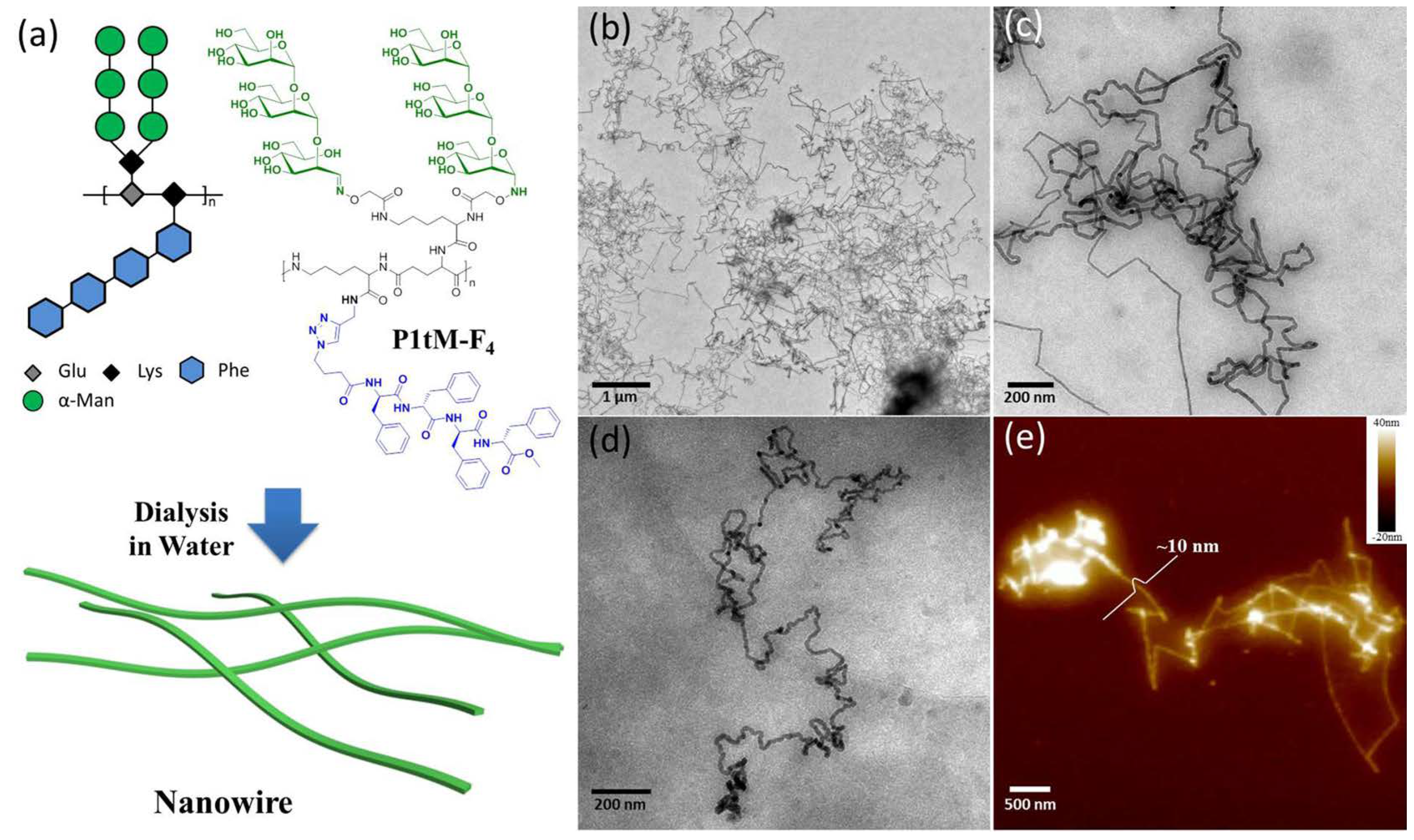
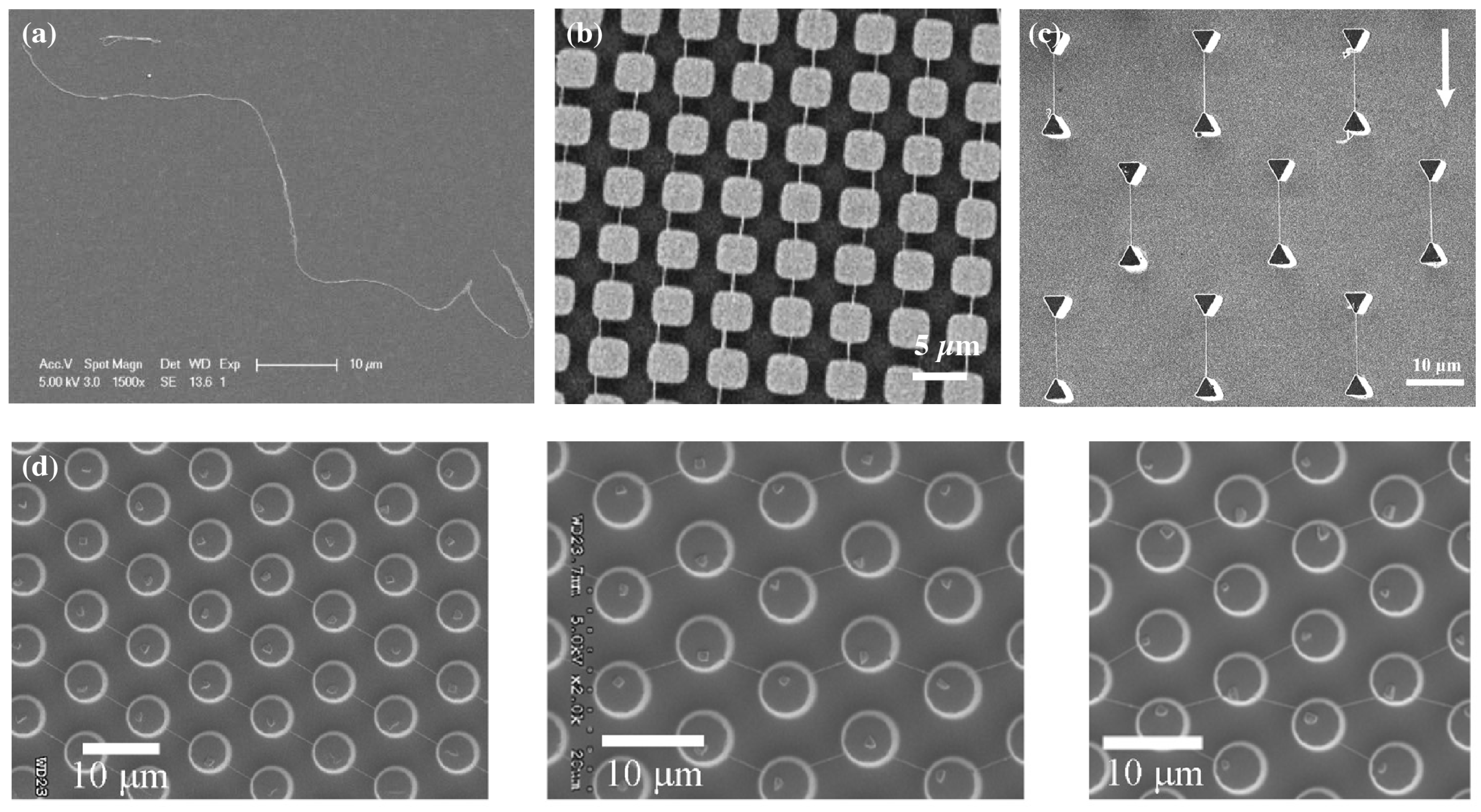
2.2. Self-Assembly of Micelles
3. Aligned Nanowires
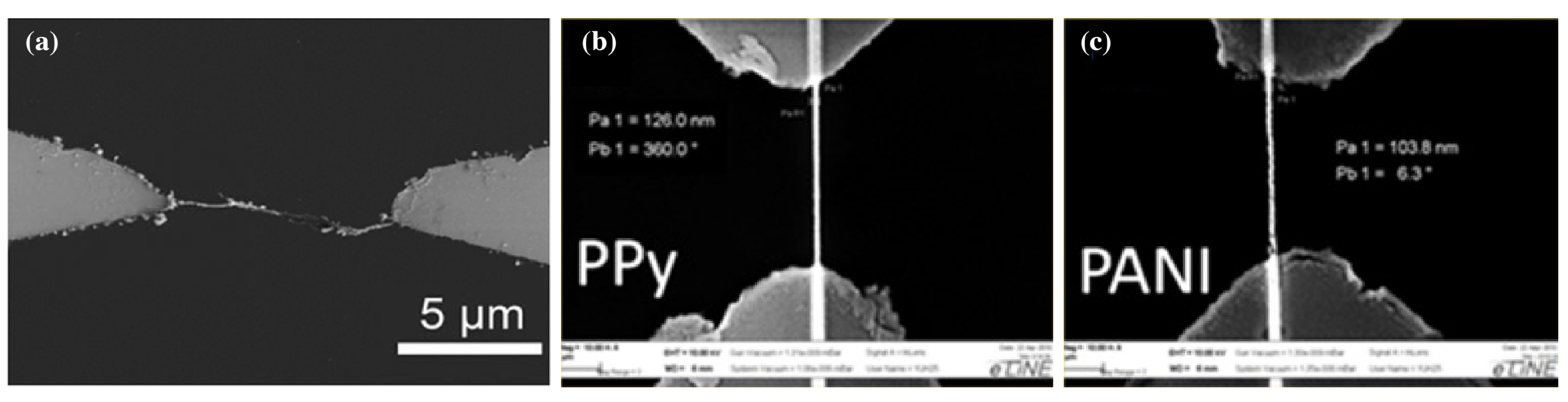
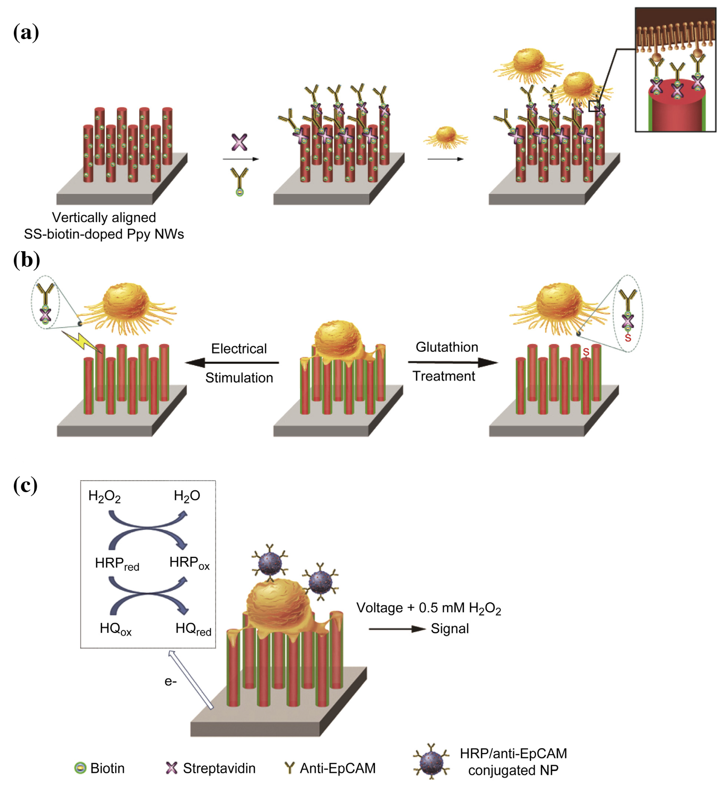
3.1. Vertical Nanowires
3.2. Micropillar Dewetting
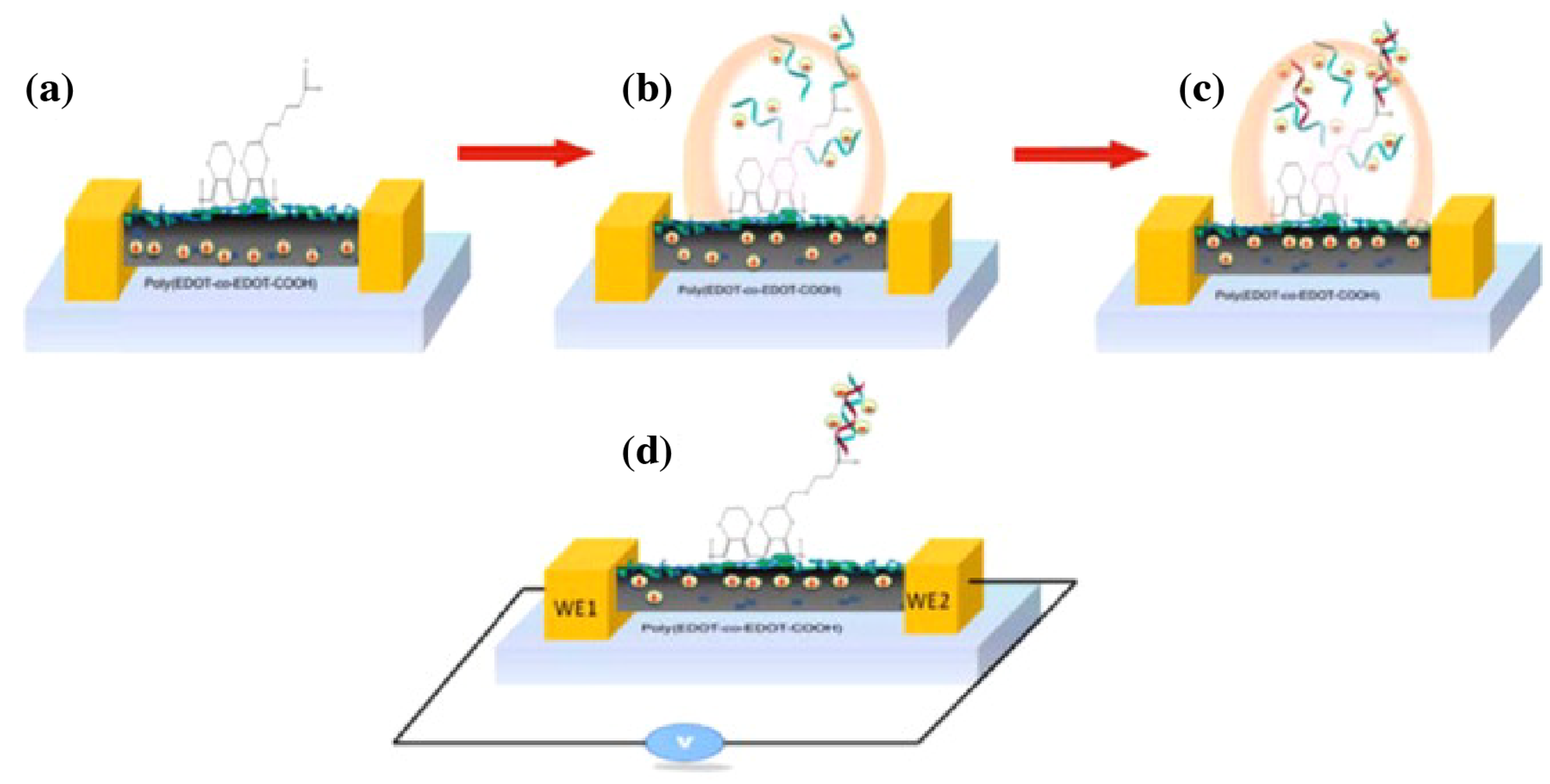
3.3. Electrosynthesizing
4. Detection Strategies and Opportunities
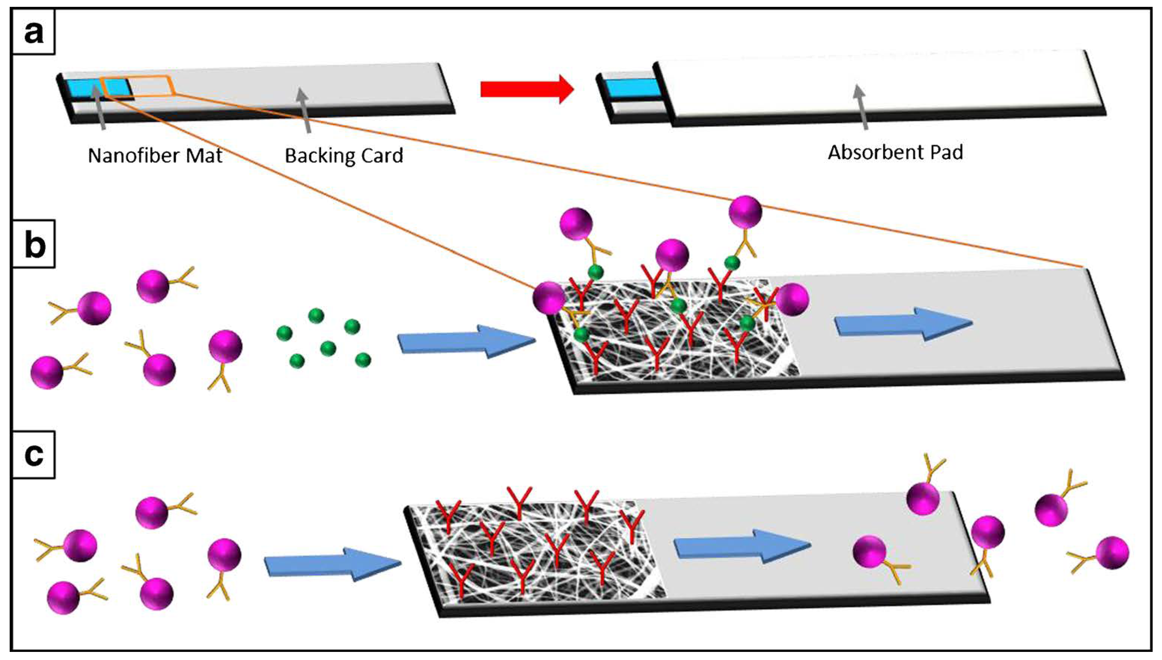
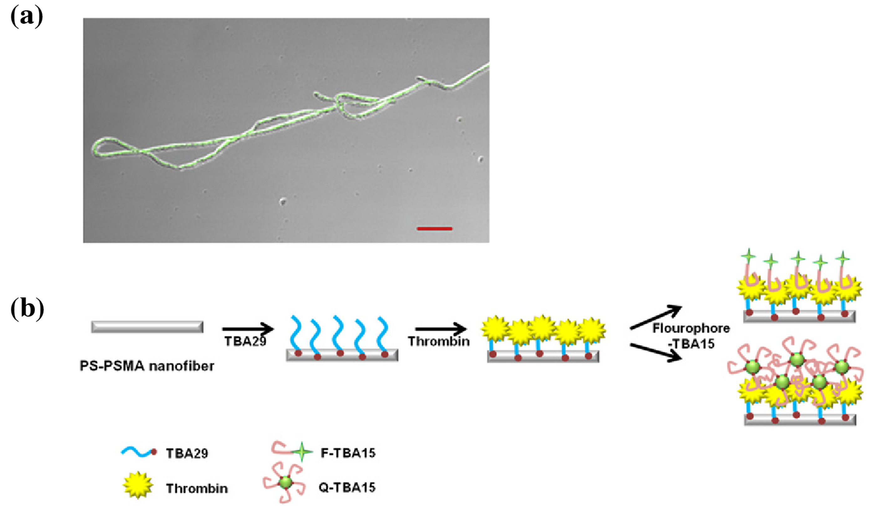
4.1. Optical
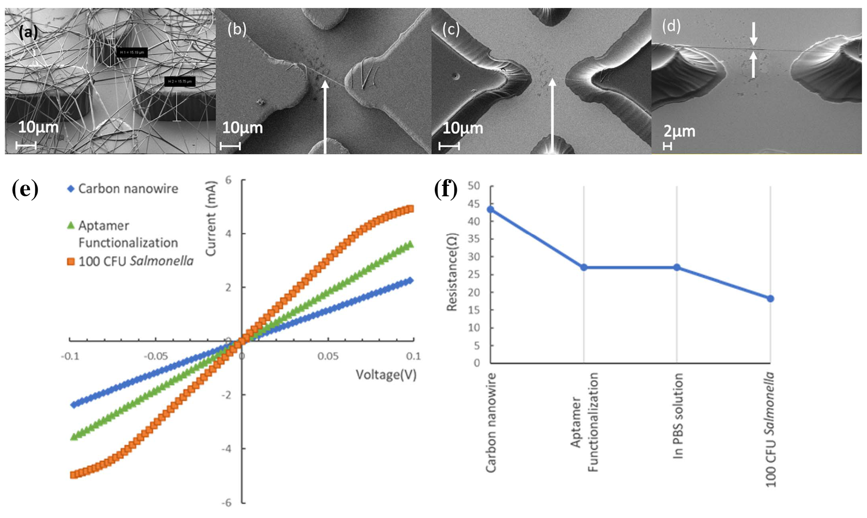
4.2. Electrical
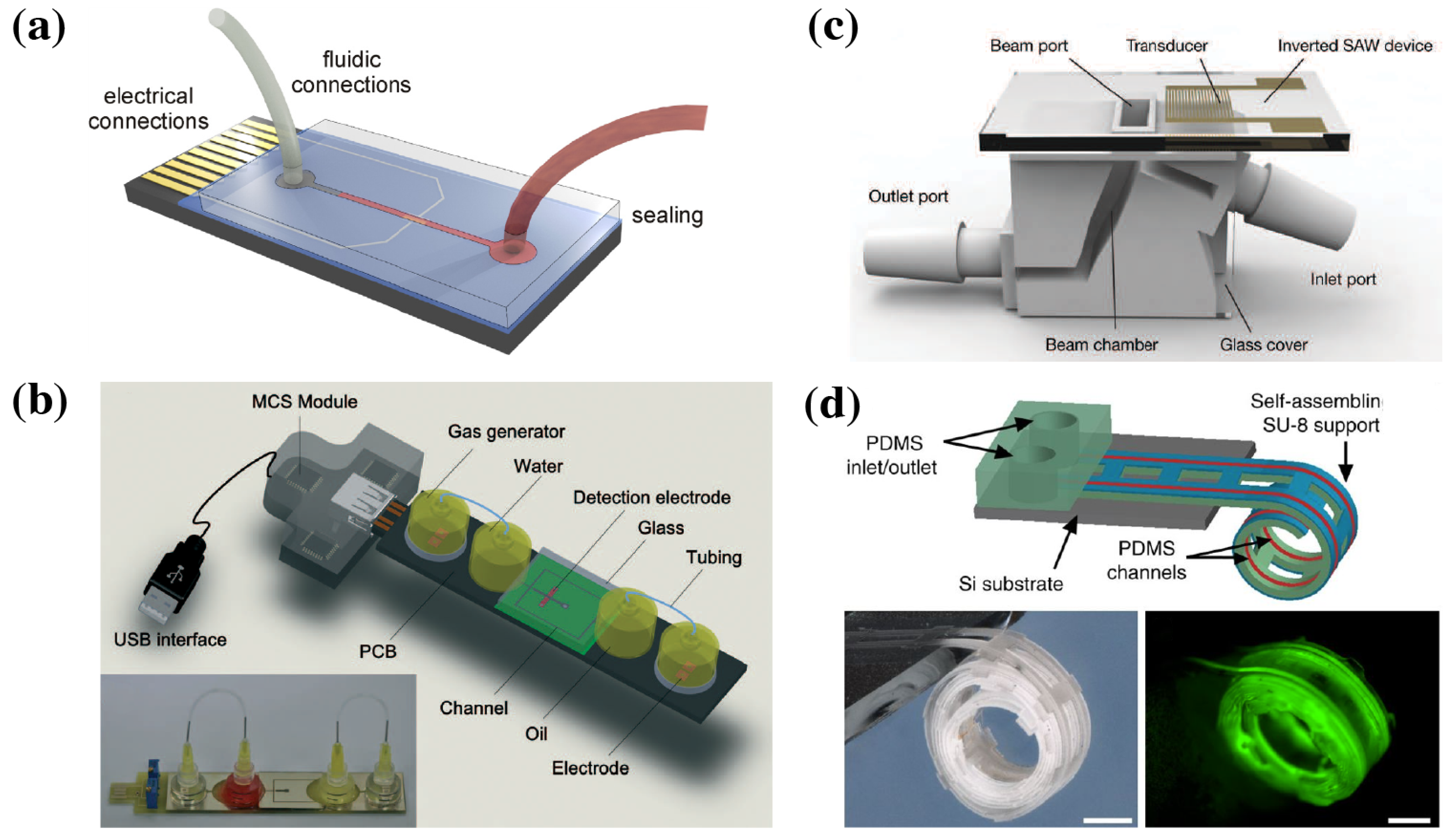
4.3. Packaging
5. Conclusions
Author Contributions
Funding
Conflicts of Interest
Abbreviations
| CFU | Colony-forming units |
| CNT | Carbon nanotube |
| CTC | Circulating tumor cells |
| EDC | 1-Ethyl-3-(3-dimethylaminopropyl)-carbodiimide |
| HRP | Horse radish peroxidase |
| ICP | Inductive coupled plasma |
| LIP | Laser interference patterning |
| NHS | N-hydroxysuccinimide |
| PANI | Polyaniline |
| PEDOT | Poly(3,4-ethylenedioxythiophene) |
| PEG | Polyethylene glycol |
| PEO | Poly ethylene oxide |
| PLA | Polylactic acid |
| PMMA | Poly(methyl methacrylate) |
| Poly(Py-co-PAA) | Poly(pyrrole-co-pyrroleacrylic acid) |
| PPy | Polypyrrole |
| PS | Polystyrene |
| PSMA | Poly(styrene-co-maleic anhydride) |
| PSS | Poly(styrene sulfonate) |
| PSS-g-ANI | Poly(styrene sulfonic acid graft aniline) |
References
- Wang, Z.; Lee, S.; Koo, K.; Kim, K. Nanowire-Based Sensors for Biological and Medical Applications. IEEE Trans. NanoBiosci. 2016, 15, 186–199. [Google Scholar] [CrossRef] [PubMed]
- Zhang, A.; Lieber, C.M. Nano-Bioelectronics. Chem. Rev. 2016, 116, 215–257. [Google Scholar] [CrossRef] [PubMed]
- Roco, M.C.; Mirkin, C.A.; Hersam, M.C. Nanotechnology research directions for societal needs in 2020: summary of international study. J. Nanopart. Res. 2011, 13, 897–919. [Google Scholar] [CrossRef]
- Patolsky, F.; Zheng, G.; Lieber, C.M. Nanowire sensors for medicine and the life sciences. Nanomedicine 2006, 1, 51–65. [Google Scholar] [CrossRef]
- Patolsky, F.; Zheng, G.; Lieber, C.M. Nanowire-Based Biosensors. Anal. Chem. 2006, 78, 4260–4269. [Google Scholar] [CrossRef]
- Tran, D.P.; Pham, T.T.T.; Wolfrum, B.; Offenhäusser, A.; Thierry, B. CMOS-compatible silicon nanowire field-effect transistor biosensor: Technology development toward commercialization. Materials 2018, 11, 785. [Google Scholar] [CrossRef]
- Cimalla, V. Label-Free Biosensors Based on III-Nitride Semiconductors. In Label-Free Biosensing; Schöning, M., Poghossian, A., Eds.; Number 16; Springer: Berlin, Germany, 2017; pp. 59–102. [Google Scholar]
- Tîlmaciu, C.M.; Morris, M.C. Carbon nanotube biosensors. Front. Chem. 2015, 3, 1–21. [Google Scholar] [CrossRef]
- Yang, N.; Chen, X.; Ren, T.; Zhang, P.; Yang, D. Carbon nanotube based biosensors. Sens. Actuators B Chem. 2015, 207, 690–715. [Google Scholar] [CrossRef]
- Chen, S.; Tang, Y.; Zhan, K.; Sun, D.; Hou, X. Chemiresistive nanosensors with convex/concave structures. Nano Today 2018, 20, 84–100. [Google Scholar] [CrossRef]
- Naveen, M.H.; Gurudatt, N.G.; Shim, Y.B. Applications of conducting polymer composites to electrochemical sensors: A review. Appl. Mater. Today 2017, 9, 419–433. [Google Scholar] [CrossRef]
- Rems, L.; Kawale, D.; Lee, L.J.; Boukany, P.E. Flow of DNA in micro/nanofluidics: From fundamentals to applications. Biomicrofluidics 2016, 10, 043403. [Google Scholar] [CrossRef]
- Rubenstein, M.; Colby, R.H. Polymer Physics; Oxford University Press: Oxford, UK, 2003. [Google Scholar]
- Yang, G.; Li, X.; He, Y.; Ma, J.; Ni, G.; Zhou, S. From nano to micro to macro: Electrospun hierarchically structured polymeric fibers for biomedical applications. Prog. Polym. Sci. 2018, 81, 80–113. [Google Scholar] [CrossRef]
- Lee, J.Y.; Kang, T.H.; Choi, J.H.; Choi, I.S.; Yu, W.R. Improved electrical conductivity of poly(ethylene oxide) nanofibers using multi-walled carbon nanotubes. AIP Adv. 2018, 8, 035024. [Google Scholar] [CrossRef]
- Malhotra, B.D.; Ali, M.A. Biopolymeric Nanostructures. In Nanomaterials for Biosensors; Elsevier: Amsterdam, The Netherlands, 2018; pp. 127–144. [Google Scholar]
- Reinholt, S.J.; Sonnenfeldt, A.; Naik, A.; Frey, M.W.; Baeumner, A.J. Developing new materials for paper-based diagnostics using electrospun nanofibers. Anal. Bioanal. Chem. 2013, 406, 3297–3304. [Google Scholar] [CrossRef]
- Çam, D.; Öktem, H.A. Optimizations needed for lateral flow assay for rapid detection of pathogenic E. coli. Turk. J. Biol. 2017, 41, 954–968. [Google Scholar] [CrossRef]
- Suria, M.S.; Mohd Afendy, A.T.; Noor Azlina, M.; Zamri, I. Lateral flow assay strip for detection of Escherichia coli O157:H7. Int. Food Res. J. 2015, 22, 2587–2593. [Google Scholar]
- Lee, S.J.; Tatavarty, R.; Gu, M.B. Electrospun polystyrene–poly(styrene-co-maleic anhydride) nanofiber as a new aptasensor platform. Biosens. Bioelectron. 2012, 38, 302–307. [Google Scholar] [CrossRef] [PubMed]
- Liu, Y.; Zhang, X.; Xia, Y.; Yang, H. Magnetic-Field-Assisted Electrospinning of Aligned Straight and Wavy Polymeric Nanofibers. Adv. Mater. 2010, 22, 2454–2457. [Google Scholar] [CrossRef]
- Kiselev, P.; Rosell-Llompart, J. Highly aligned electrospun nanofibers by elimination of the whipping motion. J. Appl. Polym. Sci. 2012, 125, 2433–2441. [Google Scholar] [CrossRef]
- Thiha, A.; Ibrahim, F.; Muniandy, S.; Dinshaw, I.J.; Teh, S.J.; Thong, K.L.; Leo, B.F.; Madou, M. All-carbon suspended nanowire sensors as a rapid highly-sensitive label-free chemiresistive biosensing platform. Biosens. Bioelectron. 2018, 107, 145–152. [Google Scholar] [CrossRef] [PubMed]
- Zheng, M.; Zheng, L.; Zhang, P.; Li, J.; Zhang, Y. Development of Bioorthogonal Reactions and Their Applications in Bioconjugation. Molecules 2015, 20, 3190–3205. [Google Scholar] [CrossRef]
- Tian, Q.; Fei, C.; Yin, H.; Feng, Y. Stimuli-Responsive Polymer Wormlike Micelles. Prog. Polym. Sci. 2018. [Google Scholar] [CrossRef]
- Jennings, L.; Waton, G.; Schosseler, F.; Mendes, E. Towards a rational morphology control of frozen copolymer aggregates. Soft Matter 2017, 13, 6090–6099. [Google Scholar] [CrossRef]
- Zhang, K.; Suratkar, A.; Vedaraman, S.; Lakshminarayanan, V.; Jennings, L.; Glazer, P.J.; van Esch, J.H.; Mendes, E. Two Robust Strategies toward Hydrogels from Quenched Block Copolymer Nanofibrillar Micelles. Macromolecules 2018, 51, 5788–5797. [Google Scholar] [CrossRef]
- Liu, Y.; Zhang, Y.; Wang, Z.; Wang, J.; Wei, K.; Chen, G.; Jiang, M. Building Nanowires from Micelles: Hierarchical Self-Assembly of Alternating Amphiphilic Glycopolypeptide Brushes with Pendants of High-Mannose Glycodendron and Oligophenylalanine. J. Am. Chem. Soc. 2016, 138, 12387–12394. [Google Scholar] [CrossRef] [PubMed]
- Glazer, P.J.; Bergen, L.; Jennings, L.; Houtepen, A.J.; Mendes, E.; Boukany, P.E. Generating Aligned Micellar Nanowire Arrays by Dewetting of Micropatterned Surfaces. Small 2014, 10, 1729–1734. [Google Scholar] [CrossRef] [PubMed]
- Zhu, J.; Hayward, R.C. Spontaneous Generation of Amphiphilic Block Copolymer Micelles with Multiple Morphologies through Interfacial Instabilities. J. Am. Chem. Soc. 2008, 130, 7496–7502. [Google Scholar] [CrossRef] [PubMed]
- Nie, X.; Cui, J.; Jiang, W. Ultralong cylindrical micelles precisely located with semiconductor nanorods by solvent evaporation-driven self-assembly. Soft Matter 2014, 10, 8051–8059. [Google Scholar] [CrossRef] [PubMed]
- Atanase, L.; Riess, G. Self-Assembly of Block and Graft Copolymers in Organic Solvents: An Overview of Recent Advances. Polymers 2018, 10, 62. [Google Scholar] [CrossRef]
- Ahmad, Z.; Shah, A.; Siddiq, M.; Kraatz, H.B. Polymeric micelles as drug delivery vehicles. RSC Adv. 2014, 4, 17028–17038. [Google Scholar] [CrossRef]
- Xu, W.; Ling, P.; Zhang, T. Polymeric Micelles, a Promising Drug Delivery System to Enhance Bioavailability of Poorly Water-Soluble Drugs. J. Drug Deliv. 2013, 2013, 1–15. [Google Scholar] [CrossRef]
- Kulthe, S.S.; Choudhari, Y.M.; Inamdar, N.N.; Mourya, V. Polymeric micelles: Authoritative aspects for drug delivery. Des. Monomers Polym. 2012, 15, 465–521. [Google Scholar] [CrossRef]
- Cho, H.K.; Cheong, I.W.; Lee, J.M.; Kim, J.H. Polymeric nanoparticles, micelles and polymersomes from amphiphilic block copolymer. Korean J. Chem. Eng. 2010, 27, 731–740. [Google Scholar] [CrossRef]
- Nakashima, K.; Bahadur, P. Aggregation of water-soluble block copolymers in aqueous solutions: Recent trends. Adv. Colloid Interface Sci. 2006, 123–126, 75–96. [Google Scholar] [CrossRef]
- Su, B.; Tian, Y.; Jiang, L. Bioinspired Interfaces with Superwettability: From Materials to Chemistry. J. Am. Chem. Soc. 2016, 138, 1727–1748. [Google Scholar] [CrossRef] [PubMed]
- Su, B.; Wu, Y.; Jiang, L. The art of aligning one-dimensional (1D) nanostructures. Chem. Soc. Rev. 2012, 41, 7832. [Google Scholar] [CrossRef] [PubMed]
- Fang, H.; Yuan, D.; Guo, R.; Zhang, S.; Han, R.P.S.; Das, S.; Wang, Z.L. Fabrication of Patterned Polymer Nanowire Arrays. ACS Nano 2011, 5, 1476–1482. [Google Scholar] [CrossRef] [PubMed]
- Fang, H.; Wu, W.; Song, J.; Wang, Z.L. Controlled Growth of Aligned Polymer Nanowires. J. Phys. Chem. C 2009, 113, 16571–16574. [Google Scholar] [CrossRef]
- Morber, J.R.; Wang, X.; Liu, J.; Snyder, R.L.; Wang, Z.L. Wafer-Level Patterned and Aligned Polymer Nanowire/Micro- and Nanotube Arrays on any Substrate. Adv. Mater. 2009, 21, 2072–2076. [Google Scholar] [CrossRef]
- Vlad, A.; Dutu, C.A.; Jedrasik, P.; Södervall, U.; Gohy, J.F.; Melinte, S. Vertical single nanowire devices based on conducting polymers. Nanotechnology 2012, 23, 025302. [Google Scholar] [CrossRef]
- Jeon, S.; Moon, J.M.; Lee, E.S.; Kim, Y.H.; Cho, Y. An Electroactive Biotin-Doped Polypyrrole Substrate That Immobilizes and Releases EpCAM-Positive Cancer Cells. Angew. Chem. Int. Ed. 2014, 53, 4597–4602. [Google Scholar] [CrossRef] [PubMed]
- Hong, W.Y.; Jeon, S.H.; Lee, E.S.; Cho, Y. An integrated multifunctional platform based on biotin-doped conducting polymer nanowires for cell capture, release, and electrochemical sensing. Biomaterials 2014, 35, 9573–9580. [Google Scholar] [CrossRef]
- Guan, J.; Yu, B.; Lee, L.J. Forming highly ordered arrays of functionalized polymer nanowires by dewetting on micropillars. Adv. Mater. 2007, 19, 1212–1217. [Google Scholar] [CrossRef]
- Lin, C.H.; Guan, J.; Chau, S.W.; Chen, S.C.; Lee, L.J. Patterning nanowire and micro-/nanoparticle array on micropillar-structured surface: Experiment and modeling. Biomicrofluidics 2010, 4, 034103. [Google Scholar] [CrossRef]
- Su, B.; Wang, S.; Ma, J.; Wu, Y.; Chen, X.; Song, Y.; Jiang, L. Elaborate Positioning of Nanowire Arrays Contributed by Highly Adhesive Superhydrophobic Pillar-Structured Substrates. Adv. Mater. 2012, 24, 559–564. [Google Scholar] [CrossRef]
- Su, B.; Wang, S.; Wu, Y.; Chen, X.; Song, Y.; Jiang, L. Small molecular nanowire arrays assisted by superhydrophobic pillar-structured surfaces with high adhesion. Adv. Mater. 2012, 24, 2780–2785. [Google Scholar] [CrossRef] [PubMed]
- Glazer, P.J.; Warringa, Q.; Bergen, L.; Boukany, P.E. Affordable techniques for fabricating large array of functional nanowires: From DNA to micellar systems. In Proceedings of the 2015 37th Annual International Conference of the IEEE Engineering in Medicine and Biology Society (EMBC), Milan, Italy, 25–29 August 2015; pp. 2187–2190. [Google Scholar]
- Jahed, Z.; Shahsavan, H.; Verma, M.S.; Rogowski, J.L.; Seo, B.B.; Zhao, B.; Tsui, T.Y.; Gu, F.X.; Mofrad, M.R.K. Bacterial Networks on Hydrophobic Micropillars. ACS Nano 2017, 11, 675–683. [Google Scholar] [CrossRef]
- Kannan, B.; Williams, D.E.; Laslau, C.; Travas-Sejdic, J. A highly sensitive, label-free gene sensor based on a single conducting polymer nanowire. Biosens. Bioelectron. 2012, 35, 258–264. [Google Scholar] [CrossRef]
- Hu, Y.; Lee, H.; Kim, S.; Yun, M. A highly selective chemical sensor array based on nanowire/nanostructure for gas identification. Sens. Actuators B Chem. 2013, 181, 424–431. [Google Scholar] [CrossRef]
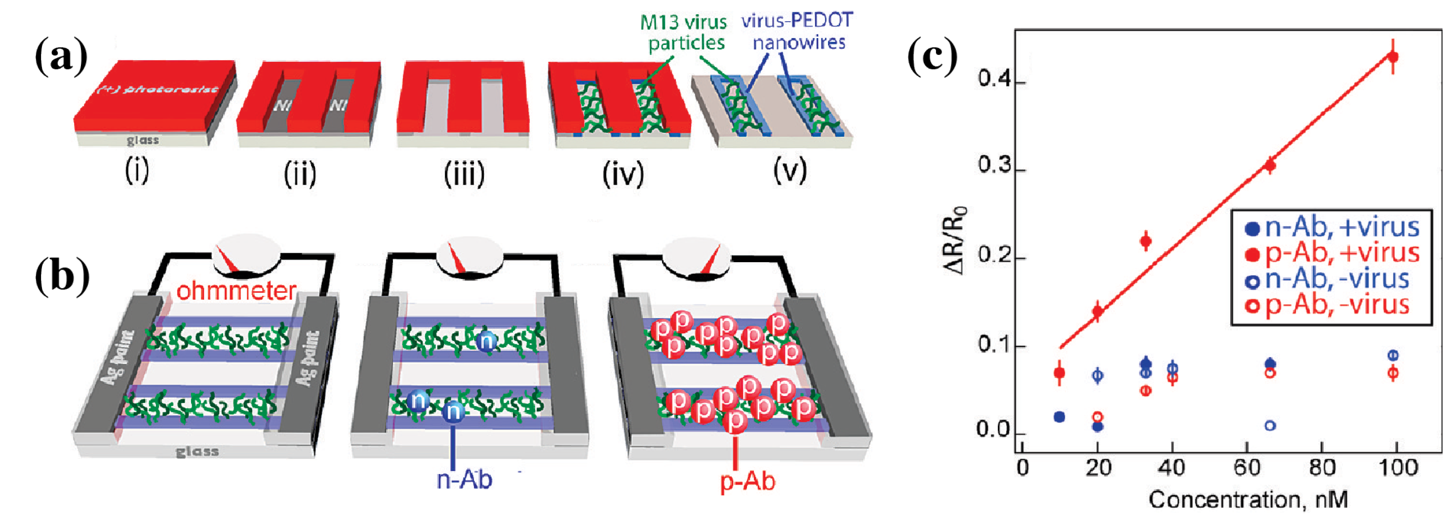
- Arter, J.A.; Taggart, D.K.; McIntire, T.M.; Penner, R.M.; Weiss, G.A. Virus-PEDOT Nanowires for Biosensing. Nano Lett. 2010, 10, 4858–4862. [Google Scholar] [CrossRef] [PubMed]
- Lee, J.O.; So, H.M.; Jeon, E.K.; Chang, H.; Won, K.; Kim, Y.H. Aptamers as molecular recognition elements for electrical nanobiosensors. Anal. Bioanal. Chem. 2008, 390, 1023–1032. [Google Scholar] [CrossRef]
- Song, S.; Wang, L.; Li, J.; Fan, C.; Zhao, J. Aptamer-based biosensors. TrAC Trends Anal. Chem. 2008, 27, 108–117. [Google Scholar] [CrossRef]
- Garcia-Cruz, A.; Lee, M.; Zine, N.; Sigaud, M.; Marote, P.; Lopez, M.; Bausells, J.; Jaffrezic-Renault, N.; Errachid, A. Biopatterning of antibodies on poly(pyrrole)-nanowires using nanocontact printing: Surface characterization. Mater. Sci. Eng. C 2018, 91, 466–474. [Google Scholar] [CrossRef] [PubMed]
- Zhu, B.; Alsager, O.A.; Kumar, S.; Hodgkiss, J.M.; Travas-Sejdic, J. Label-free electrochemical aptasensor for femtomolar detection of 17β-estradiol. Biosens. Bioelectron. 2015, 70, 398–403. [Google Scholar] [CrossRef] [PubMed]
- Wang, S.; Liu, K.; Liu, J.; Yu, Z.T.F.; Xu, X.; Zhao, L.; Lee, T.; Lee, E.K.; Reiss, J.; Lee, Y.K.; et al. Highly Efficient Capture of Circulating Tumor Cells by Using Nanostructured Silicon Substrates with Integrated Chaotic Micromixers. Angew. Chem. Int. Ed. 2011, 50, 3084–3088. [Google Scholar] [CrossRef] [PubMed]
- Lu, Y.T.; Zhao, L.; Shen, Q.; Garcia, M.A.; Wu, D.; Hou, S.; Song, M.; Xu, X.; OuYang, W.H.; OuYang, W.W.L.; et al. NanoVelcro Chip for CTC enumeration in prostate cancer patients. Methods 2013, 64, 144–152. [Google Scholar] [CrossRef] [PubMed]
- Chen, J.; Li, J.; Sun, Y. Microfluidic approaches for cancer cell detection, characterization, and separation. Lab Chip 2012, 12, 1753. [Google Scholar] [CrossRef] [PubMed]
- Kim, J.; Hong, J.W.; Kim, D.P.; Shin, J.H.; Park, I. Nanowire-integrated microfluidic devices for facile and reagent-free mechanical cell lysis. Lab Chip 2012, 12, 2914. [Google Scholar] [CrossRef]
- Nan, L.; Jiang, Z.; Wei, X. Emerging microfluidic devices for cell lysis: A review. Lab Chip 2014, 14, 1060–1073. [Google Scholar] [CrossRef]
- Chang, H.K.; Ishikawa, F.N.; Zhang, R.; Datar, R.; Cote, R.J.; Thompson, M.E.; Zhou, C. Rapid, Label-Free, Electrical Whole Blood Bioassay Based on Nanobiosensor Systems. ACS Nano 2011, 5, 9883–9891. [Google Scholar] [CrossRef]
- Walsh, D.I.; Kong, D.S.; Murthy, S.K.; Carr, P.A. Enabling Microfluidics: from Clean Rooms to Makerspaces. Trends Biotechnol. 2017, 35, 383–392. [Google Scholar] [CrossRef]
- Temiz, Y.; Lovchik, R.D.; Kaigala, G.V.; Delamarche, E. Lab-on-a-chip devices: How to close and plug the lab? Microelectron. Eng. 2015, 132, 156–175. [Google Scholar] [CrossRef]
- Li, J.; Wang, Y.; Dong, E.; Chen, H. USB-driven microfluidic chips on printed circuit boards. Lab Chip 2014, 14, 860. [Google Scholar] [CrossRef]
- Webb, D.; Hutt, D.; Hopkinson, N.; Conway, P.; Palmer, P. Packaging of Microfluidic Devices for Fluid Interconnection Using Thermoplastics. J. Microelectromech. Syst. 2009, 18, 354–362. [Google Scholar] [CrossRef]
- van den Driesche, S.; Lucklum, F.; Bunge, F.; Vellekoop, M. 3D Printing Solutions for Microfluidic Chip-To-World Connections. Micromachines 2018, 9, 71. [Google Scholar] [CrossRef] [PubMed]
- Dentry, M.B.; Friend, J.R.; Yeo, L.Y. Continuous flow actuation between external reservoirs in small-scale devices driven by surface acoustic waves. Lab Chip 2014, 14, 750–758. [Google Scholar] [CrossRef] [PubMed]
- Waheed, S.; Cabot, J.M.; Macdonald, N.P.; Lewis, T.; Guijt, R.M.; Paull, B.; Breadmore, M.C. 3D printed microfluidic devices: enablers and barriers. Lab Chip 2016, 16, 1993–2013. [Google Scholar] [CrossRef] [PubMed]
- Jamal, M.; Zarafshar, A.M.; Gracias, D.H. Differentially photo-crosslinked polymers enable self-assembling microfluidics. Nat. Commun. 2011, 2, 527. [Google Scholar] [CrossRef]


| Publication | Target | Sensor | Read-Out | Range of Detection |
|---|---|---|---|---|
| Thiha et al. [23] | Salmonella bacteria | Aptamer on carbon wire | Resistance change while wet | 10 CFU/mL |
| Reinholt et al. [17] | E. coli bacteria | Antibody on nanowire mat | Colorimetric | 3.8 × 10⁶ cells/mL |
| Hong et al. [45] | Circulating tumor cells | Antibody on PPy | Amperometric | 10 cells/mL |
| Kannan et al. [52] | DNA oligo | DNA oligo on PEDOT | Resistance change after drying | 0.1 fM |
| Garcia-Cruz et al. [57] | Interleukin-10 protein | Antibody on PPy | Fluorescence (for proof-of-concept) | 250 ng/mL |
| Lee et al. [20] | Thrombin protein | Aptamer on PS-PSMA | Fluorescence | 10 pM with QD |
| Zhu et al. [58] | Estradiol protein | DNA Aptamer on Py-co-PAA membrane | Electrochemical impedance spectroscopy | 1 fM |
© 2019 by the authors. Licensee MDPI, Basel, Switzerland. This article is an open access article distributed under the terms and conditions of the Creative Commons Attribution (CC BY) license (http://creativecommons.org/licenses/by/4.0/).
Share and Cite
Hubbe, H.; Mendes, E.; Boukany, P.E. Polymeric Nanowires for Diagnostic Applications. Micromachines 2019, 10, 225. https://doi.org/10.3390/mi10040225
Hubbe H, Mendes E, Boukany PE. Polymeric Nanowires for Diagnostic Applications. Micromachines. 2019; 10(4):225. https://doi.org/10.3390/mi10040225
Chicago/Turabian StyleHubbe, Hendrik, Eduardo Mendes, and Pouyan E. Boukany. 2019. "Polymeric Nanowires for Diagnostic Applications" Micromachines 10, no. 4: 225. https://doi.org/10.3390/mi10040225
APA StyleHubbe, H., Mendes, E., & Boukany, P. E. (2019). Polymeric Nanowires for Diagnostic Applications. Micromachines, 10(4), 225. https://doi.org/10.3390/mi10040225