Article

Nanometer Gap in Electromechanical Converters—A Way to Achieve an Extremely High Energy Density

by
Igor L. Baginsky
and
Edward G. Kostsov
*
Institute of Automation and Electrometry, Siberian Branch, Russian Academy of Sciences, 630090 Novosibirsk, Russia
*
Author to whom correspondence should be addressed.
Micromachines 2019, 10(11), 746; https://doi.org/10.3390/mi10110746
Submission received: 2 October 2019 / Revised: 29 October 2019 / Accepted: 30 October 2019 / Published: 31 October 2019

Abstract

:
The analysis of electromechanical energy converters based on metal-thin film ferroelectric (with a large specific capacitance)-nanogap-moving electrode structures was performed. It was shown that the density of the energy being converted and its absolute value increase with the decreasing gap value between the surfaces of the ferroelectric and the metallic moving electrode up to nanometer values. The effects limiting the growth of this energy were established, and the limiting value of the energy density transformed in the nanogap of these structures was determined to be about 1.6 × 10¹⁰ J/m3, which is 4 orders of magnitude higher than the energy density in inductive converters. The experimental verification of this model based on the data for micromotors fabricated on these structures is given.

Graphical Abstract

1. Introduction

Electromechanical energy converters (motors and generators) that are widely used in all fields of human activity and in industry are divided into three classes: inductive, piezoelectric, electrostatic (electrical) machines, in which direct and reverse conversion of magnetic or electric field energy to mechanical energy is performed. The specific and absolute power of energy converters are determined by the energy density of the field in the working gap.
In the best inductive converters the magnetic field energy density in the gap reaches WV = 1/2 B2/μ0 = 4 × 10⁵–106 J/m3 (where μ0 is the magnetic constant) at the maximum possible values of magnetic induction, B, (of the order of 1–1.5 T) for magnetic circuits created on the basis of ferromagnets. In this case minimum gaps between the rotor and stator, determined by the production technology, are of the order of fractions of a millimeter, less than 100–300 μm [1].
Piezoelectric energy converters with respect to field energy density are comparable to electromagnetic ones, see, for example, devices based on PZT ceramics [2]. In such converters, the working gap is the material of the piezoelectric itself. The energy density in it can be high due to the large value of its dielectric constant, ε, as well as large values of the electromechanical coupling coefficient, of the order of 0.5–0.8. However, for such converters, the value of the maximum energy density being converted is not limited by the maximum field that can be formed in the dielectric without breakdown, but it is limited by the value of the mechanical stress of the material, above which an irreversible deformation of the piezoelectric occurs: σ = Fe/S (where Fe is the elastic force, S is the converter area): WV = 1/2 σ2/EY (where EY is the Young’s modulus of the material) [3].
In capacitive electrostatic energy converters, the specific volume energy density, WV, is also determined by the electric field strength in the working gap Ee:
W V = ε 0 E e 2 2 = ε 0 V e 2 2 d e 2 = C e V e 2 2 d e
where Ve is the voltage applied to the gap, de is the gap width, Ce = ε0/de is the specific (per unit area) gap capacity, ε0 is the dielectric constant of vacuum. The total energy per unit area of the structure WS is equal to:
W S = C e V e 2 2 = ε 0 V e 2 2 d e
Classical electrostatic, capacitive, energy converters have not yet found wide application because of the low specific energy density WV ≈ 40 J/m3. WV is determined by the low electric field strength Ee in the working gap of the metal-gap-metal structure (MGM), which is limited by the value of the breakdown field strength of the gap Eb. This value is known to be equal to 3 × 10⁶ V/m for air at atmospheric pressure.
An increase in the field strength in the gap can be achieved by introducing an additional dielectric layer into the MGM structure, i.e., by the use of metal-dielectric-gap-metal structures (MDGM). The introduction of a dielectric layer, which suppresses the development of breakdown, makes it possible to increase the voltage applied to the structure to several hundred volts with small gaps, of the order of 10–30 μm, see, for example, [4]. Due to this, an energy density comparable to one characteristic for large inductive converters was reached.
The work of capacitive electrostatic energy converters is based on the shift of the moving electrode (ME) in the metal- dielectric- gap- ME structure either under the action of electric field forces (motor [5,6]) or under the action of mechanical force against the electric field forces (generator [7]). The shift of the moving electrode can be carried out both in in-plane structures (in this case, the electrode overlap area is modulated without changing the gap between the ME and the dielectric), and in out-of-plane ones (the gap changes at the constant electrode area). It should be noted that in known MDGM structures further growth of the density of converted energy due to decrease of the gap width up to the nanometer scale is not realized, because in these conditions the field in the gap does not practically increase. Under small values of gap width comparable or less than dielectric film thickness the voltage V applied to the structure is distributed in such a way that only a small part of it is applied to the gap. Therefore, the only way to increase the energy density in the gap of MDGM structures is to increase the applied voltage V to the values, limited by the breakdown of the dielectric layer, see, for example, [8,9].
Obviously, it is necessary to use dielectric materials with a high value of ε and high breakdown voltage values in order to decrease the voltage drop in the dielectric when the width of the gap is decreased to nanometer scale. Such properties are characteristic for ferroelectric thin films, for which the breakdown field strength reaches 100–350 V/μm with ε being in the range of 1000–5000, see, for example, the review in [10]. High values of ε, more than 2000, are also characteristic for barium-strontium niobate (BSN) films with the composition Ba0.5Sr0.5Nb2O6 [11], which were deposited by us earlier by high-frequency sputtering on the surfaces of silicon and sapphire substrates with a sublayer of a conducting electrode indium tin oxide (ITO) or Pt, they have breakdown voltages of about 100 V/μm.
The purpose of this work is to determine the limiting density of electromechanical energy conversion in metal-ferroelectric-gap-metal structures (MFGM), with the smallest possible gap (nanometer-wide) between the metal and the ferroelectric.

2. Materials and Methods

The analysis of possible limiting operating modes of electromechanical capacitive energy converters based on MDGM-structures in order to determine the maximum energy density in the gap, and, accordingly, the maximum value of the converted energy, will be carried out using well-known literature data describing both the breakdown of nano-gaps and the current flow through them.
An experimental verification of the obtained results will be carried out on the basis of our previously obtained results on prototyping and investigation of film petal micromotors made on the basis of the metal-thin film NBS-gap-free thin metal film (petal) structures.

3. Results

3.1. Estimation of the Limiting Energy Density in Electromechanical Converters

The maximum energy density WS,max in the capacitive energy converter under consideration is determined by the following parameters: the minimum gap between the surfaces of the moving electrode and the ferroelectric de,min (and, accordingly, the maximum capacitance of the gap layer Ce,max) and the maximum voltage Vmax. Vmax is the voltage that can be applied to a MFGM-structure without its breakdown and without the onset of currents in the gap, that result in charge accumulation on the surface of the ferroelectric and, consequently, in the field decrease in the gap Ee.
The breakdown of both air and vacuum gaps in the metal-gap-metal (MGM) structure was studied quite intensively. А large number of papers devoted to the breakdown of micron and submicron gaps was published earlier, see, for example, reviews in [12,13,14].
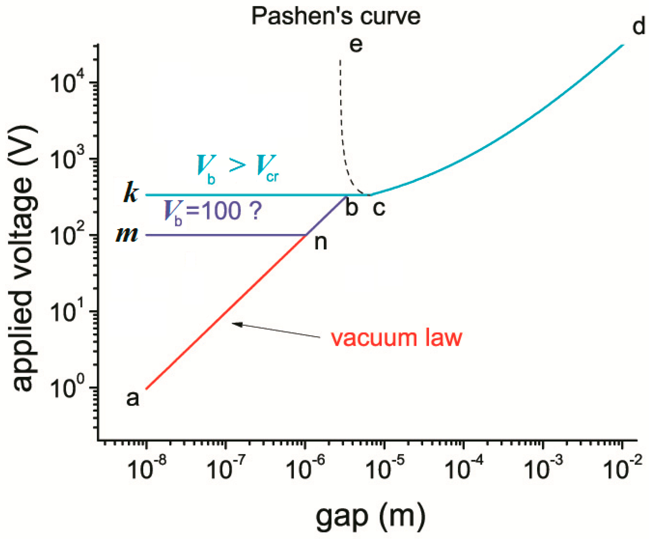
Studies of the MGM structures show that at atmospheric pressure, starting from gaps of 7 μm and less, there is a deviation from the classical Paschen breakdown law (ecd curve, Figure 1): The dependence of the critical voltage Vcr, which in this case is equal to the breakdown voltage of the structure Vb, from the gap width de is a plateau (bc curve on the Vcr(de) curve). Then At de < 3 μm Vcr decreases linearly with decreasing de from Vi = 330 V in the plateau region to 1 V at de = 10 nm, curve ab [12] (see curve abcd in Figure 1). This behavior of Vcr is explained by the change in the breakdown mechanism: from impact ionization described by the Paschen law (curve ecd) to the breakdown by the vacuum mechanism (curve ab), which is typical for small gaps at which the ionization length exceeds the width of the gap. Under the conditions of the vacuum mechanism the breakdown is determined by a sharp increase in the concentration of electrons injected from micro-spikes on the electrode surface [15]. In particular, when micro-spikes are smoothed out by melting, the breakdown voltage increases several times [16,17], remaining relatively small in magnitude.
For the out-of-plane structures nanometer-sized minimum gaps are possible. Let us consider the features of the operation of such energy converters.
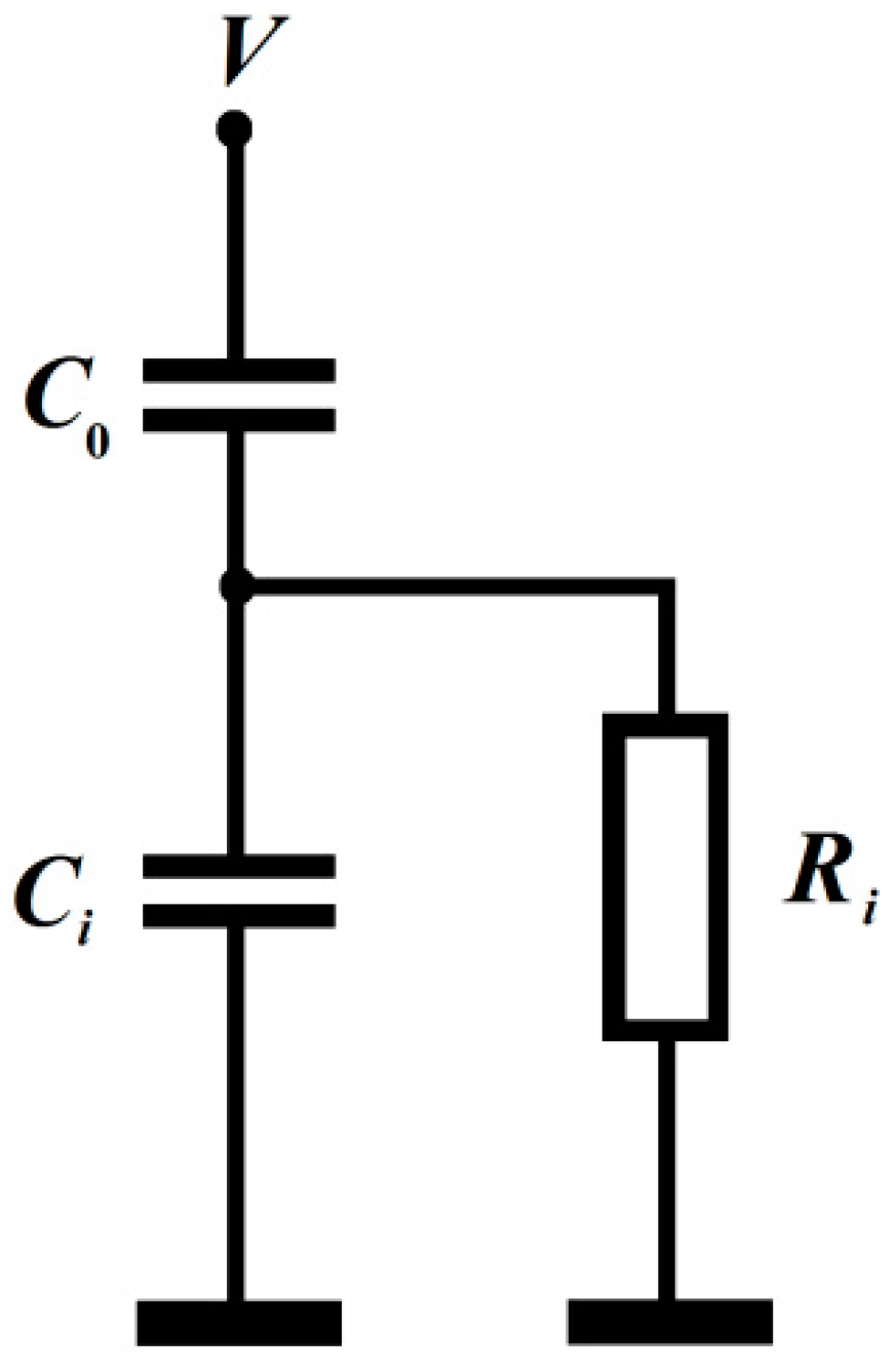
MDGM-structure can be represented as a serial connection of two capacitances of the dielectric layer CF and the air gap Ce, Figure 2. In this case, the voltage drop across the air gap is expressed as:
V e = V C F C e + C F = V d F ε d e + 1 = V d e d e *
d e * = d F / ε + d e
In the case when CF<<Ce or dF/ε>>de, we have Ve<<V. So, the most part of the voltage applied to the structure falls on the dielectric layer. Since the dielectric constant of linear dielectrics usually does not exceed 2–10, if the dielectric thickness is about 2–20 μm, which is necessary to prevent breakdown of the structure, reducing the gap to values less than 1 μm will reduce the fraction of voltage applied to the gap. In this case, as de decreases, the energy density WV, calculated in accordance with Equation (1), does not increase, since the field in the gap does not change and is equal to:
E e 1 = V d F / ε
The total energy per unit area WS (see Equation (2)) decreases in accordance with the decrease in the voltage drop across the gap:
V e 1 = V ε d e d F
Thus, to increase the energy density, as well as the total energy of a capacitive energy converter by reducing the gap between the surfaces of the moving electrode and the dielectric the opposite condition should be fulfilled: CF >> Ce or dF/ε << de. In this case, almost all the voltage is applied to the gap: VeV. Since the thickness of the dielectric should be in the range of a few microns (according to the conditions for maintaining the electrical strength of the structure), its dielectric constant must be higher than 1000. This means that in order to reach high energy in converters based on MDGM structures, it is necessary to use ferroelectric thin films with a high dielectric constant value as a dielectric layer. In this case the de value can be reduced to 5–20 nm.
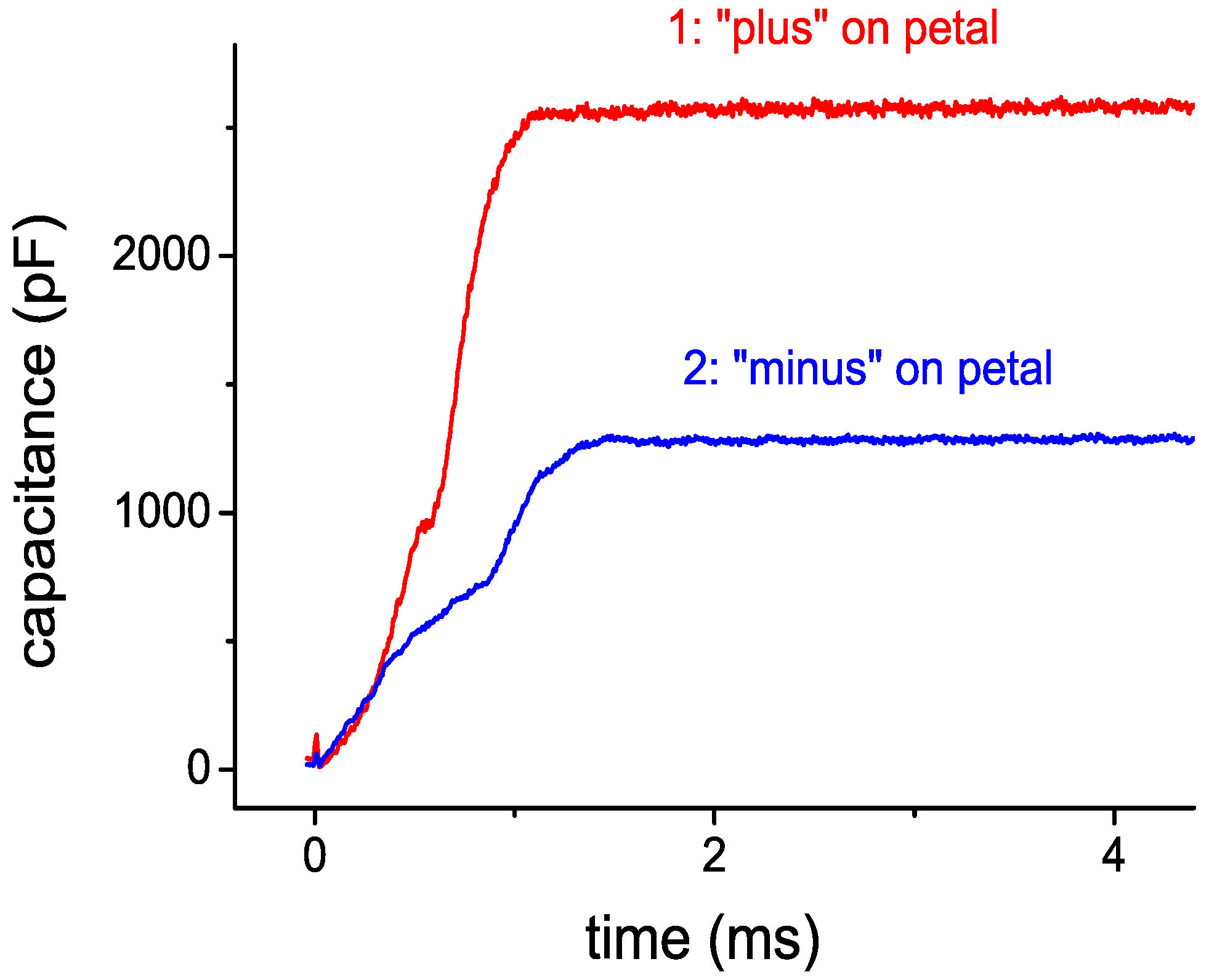
Let us estimate the maximum electric field strength Emax in the nano-gaps of these structures and the maximum energy density. It is clear that this value should be dependent on the polarity of the voltage applied to the moving electrode if the values of field strength in the nanogap are very high. At negative voltages the current of autoelectron emission flowing from the ME surface through a tunnel-transparent gap to the surface states of the ferroelectric film may occur, giving rise to field screening in the nano-gap by charge accumulation on this surface. Such a process was previously observed experimentally in the study of the memory effect in structures based on thin films of silicon nitride with a sublayer of a tunnel-transparent layer of silicon dioxide [18]. When electrostatic micromotors have been investigated (see [19]), this effect manifested itself in charge accumulation at the gap-ferroelectric interface even when sufficiently small (less than 50 V) negative voltages were applied to the moving electrode of the MFGM structure. In particular, the force of electrostatic attraction of ME to the surface of a ferroelectric decreases leading to a corresponding decrease in the capacitance of the structure, as compared with the case of positive displacement, see Figure 3. Note that for micromotors the effect of charge accumulation in the ferroelectric layer causes the slider to slow down up to total shutdown.
If the mobile electrode is at a positive potential relative to the opposite electrode, then the mechanisms limiting the magnitude of the field in the gap are the effects of field evaporation of metal atoms from the electrode surface and electron tunneling directly from the ferroelectric valence band [20,21]. According to estimates, the magnitude of the field, starting from which these effects are significant, is Ecr = 6 × 10¹⁰ V/m [20,21].
It is easy to show that for parameters characteristic for a ferroelectric film: ε/d = 109 (μm)−1 or CF = 8.85 × 10⁻³ F/m2, the field in the gap of 5 nm in width can reach 1010–6 × 10¹⁰ V/m. Then, in the absence of field screening in the gap (for example, when the structure is placed in vacuum) and with a sufficiently high breakdown voltage of the ferroelectric layer, the maximum density of electrical energy in the nanogap of the MFGM structure is equal to WV,max = 1.6 × 10¹⁰ J/m3, see Equation (1), and the energy per unit area can reach WS,max = 80 J/m2, respectively.
Thus, the value of WV,max for the considered capacitive converters exceeds the energy density of the inductive converters by 4 orders of magnitude. It is also easy to show (see Equation (2)) that for conventional electrostatic generators on MGM structures the value of total energy WS,max, comparable to that estimated above for MFGM-structures, can be reached only with an interelectrode gap equal to 2 m and the applied voltage of 106 V.

3.2. Peculiarities of Operation of the Electromechanical Transducer in the Modes of Limiting High Energy Density in the Nanogap

Let us consider electromechanical transducers in which the gap is modulated by the movement of ME from the minimum (nanometer) value de,min to a certain value de,max. Depending on the conditions in the environment, there are two possible modes of operation of the energy converter based on the MFGM structure, which we will further call as “atmospheric” and “vacuum”. For the atmospheric mode, when the minimum gap changes from nanometer values of de,min during ME oscillations with amplitudes de,max exceeding de,cr = 3 μm, the air ionization in the gap occurs, starting from Ve = Vi, see Figure 1, which is absent in the vacuum mode. The vacuum mode can also manifest itself at atmospheric air pressure, when the impact ionization length exceeds the maximum width of the gap, i.e. with the ME oscillation amplitude being less than de,cr.
Under conditions of the atmospheric mode, and when the breakdown voltage of a ferroelectric Vb is less than the minimum voltage on the Paschen curve Vi, the dependence of the maximum possible voltage in the MFGM structure on the gap size is described by the curve mnbcd, Figure 1. If Vb > Vi, then as the gap increases starting from 3 μm to 7 μm air is ionized in the gap by the impact ionization mechanism. It leads to the formation of a screening charge on the surface of the ferroelectric, which reduces the power consumption of the converter. In this case, the electric field in the gap, see [22], is expressed as:
E e = Q S / ε 0 = C ( V V P ) / ε 0
where QS is the charge on ME, VP = QP/CF, QP is the charge accumulated at the gap-dielectric boundary. The attraction force of the electric field acting on the moving electrode is:
F = 1 2 Q S E e = Q S 2 S 2 ε 0
and the energy converted in the structure is:
W S = Q S 2 2 C = C ( V V P ) 2 2
It is clear, that the process of charge accumulation QP will be stopped, when the voltage drop across the gap Ee × de (see Equation (7)) reaches the impact ionization potential Vi, when:
V = V cr = d e * d e V i
Then:
E e , cr = d e * d e C V i / ε 0
Therefore, in the case under consideration, the energy conversion is described by the curve kcd, Figure 1, and the maximum energy produced during the conversion cycle is:
W S , max = C max V i 2 2 ( d e * d e ) 2
where:
C max = C e , max C F C e , max + C F = ε 0 S d e *
Thus, the critical voltage Vcr is equal to Vb when ferroelectric films with a high value of ε are used in MFGM structures and under the conditions Vb < Vi,. As the applied voltage reaches this value, a breakdown of the structure occurs. When Vb > Vi, the critical voltage is calculated by Equation (10), it is equal to the ionization potential Vi. When this voltage is exceeded, impact air ionization in the gap begins, leading to the formation of a charge that screens the field in the gap.
Let us estimate the maximum density of electrical energy that can be reached in converters based on MFGM structures. Assuming that de = 5 nm, d = 1 μm, ε = 1000 (or ε/d = 109 m−1, CF = 8.85·10−3 F/m2) and taking into account that Vi = 330 V, we obtain: de* = 6 nm, C = 1.48 × 10⁻³ F/m2 and WS,max = 80 J/m2 and WV,max = 1.6 × 10¹⁰ J/m3, correspondingly.
Note that these estimates of the limiting energies WS,max and WV,max coincide with their values for the vacuum breakdown mode and at a gap size of 5 nm, when the energy is limited by some critical field in the gap Ecr. When Ee > Ecr the evaporation of metal atoms from the surface of PE by the electric field starts. According to [20,21], the value of this field can be estimated as 6 × 10¹⁰ V/m. In particular, for atoms of copper, lanthanum and zinc, it is equal to 3 × 10¹⁰ V/m, for tungsten atoms it reaches 1011 V/m. It can be noted that there are no restrictions on the value of WS,max in this mode associated with the ionization of air in the gap, so it increases with the growth of the gap width, see Equation (2):
W S , max = ε 0 E e , cr 2 d e 2
with the bulk energy density WV,max = 1.6 × 10¹⁰ J/m3 being constant.
In this case, the parameters limiting the growth of WS,max are both the electrical strength of the ferroelectric, limiting the voltage applied to the MFGM structure, and the increase in the conduction current in the gap, which screens the field in it. The conduction current through the nanogap increases starting from some critical width de,cr, at which the ion-electron emission current arises [23]. The mechanism of this emission lies in the injection of electrons from the valence band of a ferroelectric into the vacuum gap when a metal ion pulled by the field from the moving electrode strikes the surface of the ferroelectric. Since it is known [23] that such emission begins at an ion velocity v of the order of 107 m/s, then, based on the energy balance, the critical gap value will be equal to:
d e , cr = m v 2 2 e E cr
In particular, for the copper atom de,cr = 50 nm.
Thus, in the vacuum mode, it is possible to increase, practically by an order of magnitude, the values of the energy WS,max, compared to the atmospheric mode.

3.3. Examples of Practical Implementation of Energy Converters on MFGM-Structures. Experimental Evaluation of Maximum Energy Density

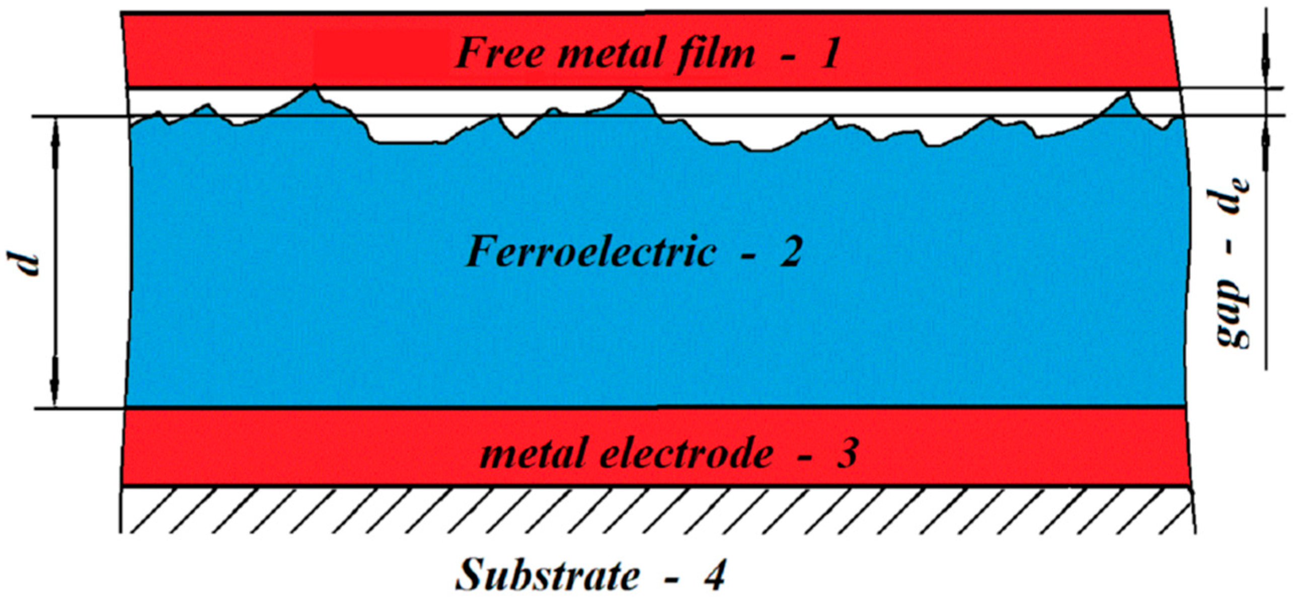
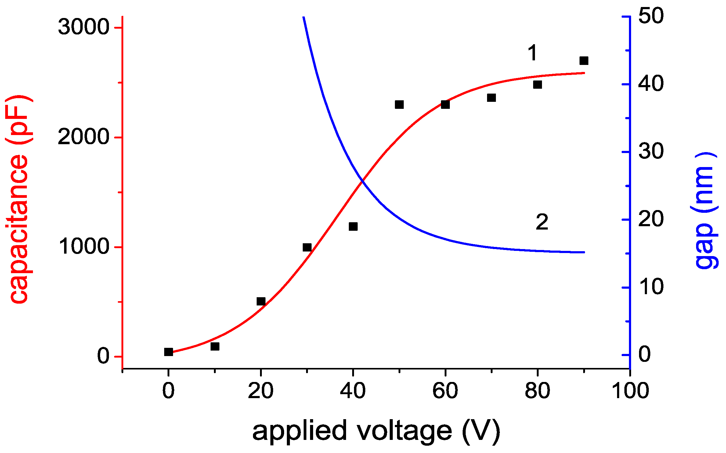
An example of a MFGM structure with a nano-gap created using the electrostatic attraction of a free metal film to the surface of a ferroelectric [19,24] is shown in Figure 4. The minimum size of the gap is determined both by the dimensions of microspikes on the surface of the ferroelectric (ranging from 5 to 50 nm), and by the force of electrostatic attraction of the metal film to the surface, which depends on the amplitude of the applied voltage, Figure 5, see [25].
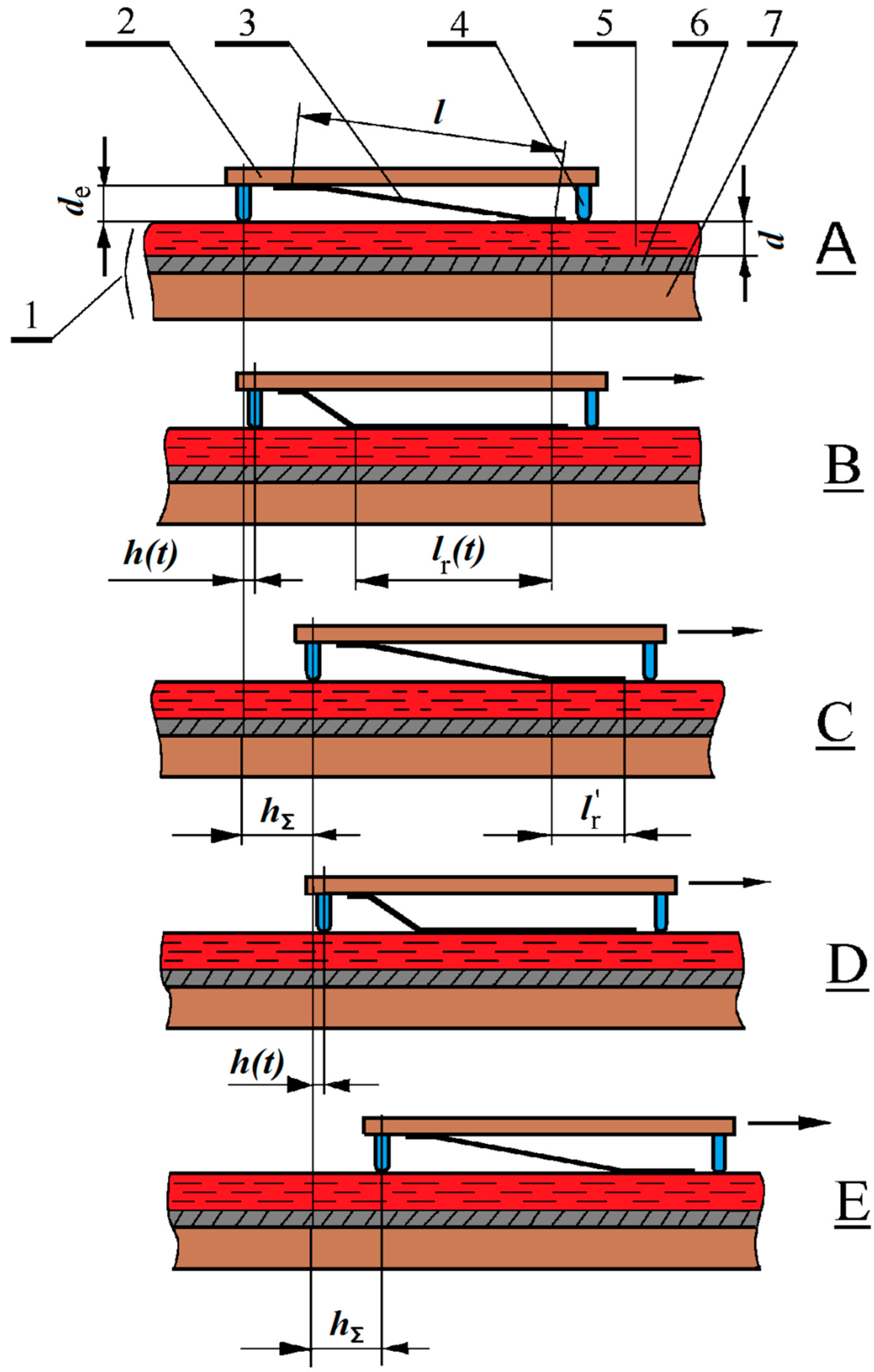
The design of an electrostatic micromotor, which was developed by us earlier [19,24,25,26,27]. Some of these designs were patented [28,29]. Figure 6, can serve as an example of an energy converter based on a MFGM structure with a nano-gap that develops high mechanical forces.
The operation of such micromotors is based on the successive attraction by electrostatic forces (section by section) of a free metal film (petal) to the ferroelectric surface with an electrode underlayer deposited on the substrate resulting in the formation of a nanometer gap, see Figure 6.
The stationary plate (stator) I consists of the silicon substrate 7 with the electrode 6 and ferroelectric film 5 deposited on it’s surface. The moving plate (rotor) 2 is separated from the stator by the gap 4. The metallic petals 3 with the length equal to I are synthesized on the rotor’s surface. Rotor moves with respect to the stator along the guides 4.
When the pulse is applied between the petal 3 having it’s initial position A and the electrode 6, the part of the petal is rolled to the ferroelectric surface (state B). The metallic film bends, stretches and transfers the movement to the plate 2, thus carrying out the electromechanical energy conversion. The rolling length lr(t) increases as the voltage pulse acts, and, therefore, rotor’s shift h(t) varies with the voltage pulse duration t. After the end of voltage pulse action the petal under the effect of the elastic force comes to it’s initial position A (with a single voltage pulse) or to the new position C, typical to the continuous rotor movement (when a series of the pulses is applied to the sample),and the rotor is moving by means of inertia to the distance hΣ. The duration of this process defines space between the voltage pulses, i.e. the maximum frequency of these pulses, of order (ρ is the specific weight of petal material, dP is te petal width, l is it length, EY – Yong’s modulus), and, consequently, the power output of the micromotor. When the second voltage pulse is applied to the sample the moving plate with the petals makes one more step and comes to the position D. After the end of the pulse under the effect of the inertia the rotor comes to position E (and the petals’ configuration comes to the state analogous to C).
f 0 0.162 d P l 2 E Y ρ
When the third and further pulses come, the movement occurs in the similar way: ftom position B to position C with the corresponding movement of the plate 2 This work describes the basic characteristics of the electrostatic micromotors and the peculiarities of their functioning in the step mode.
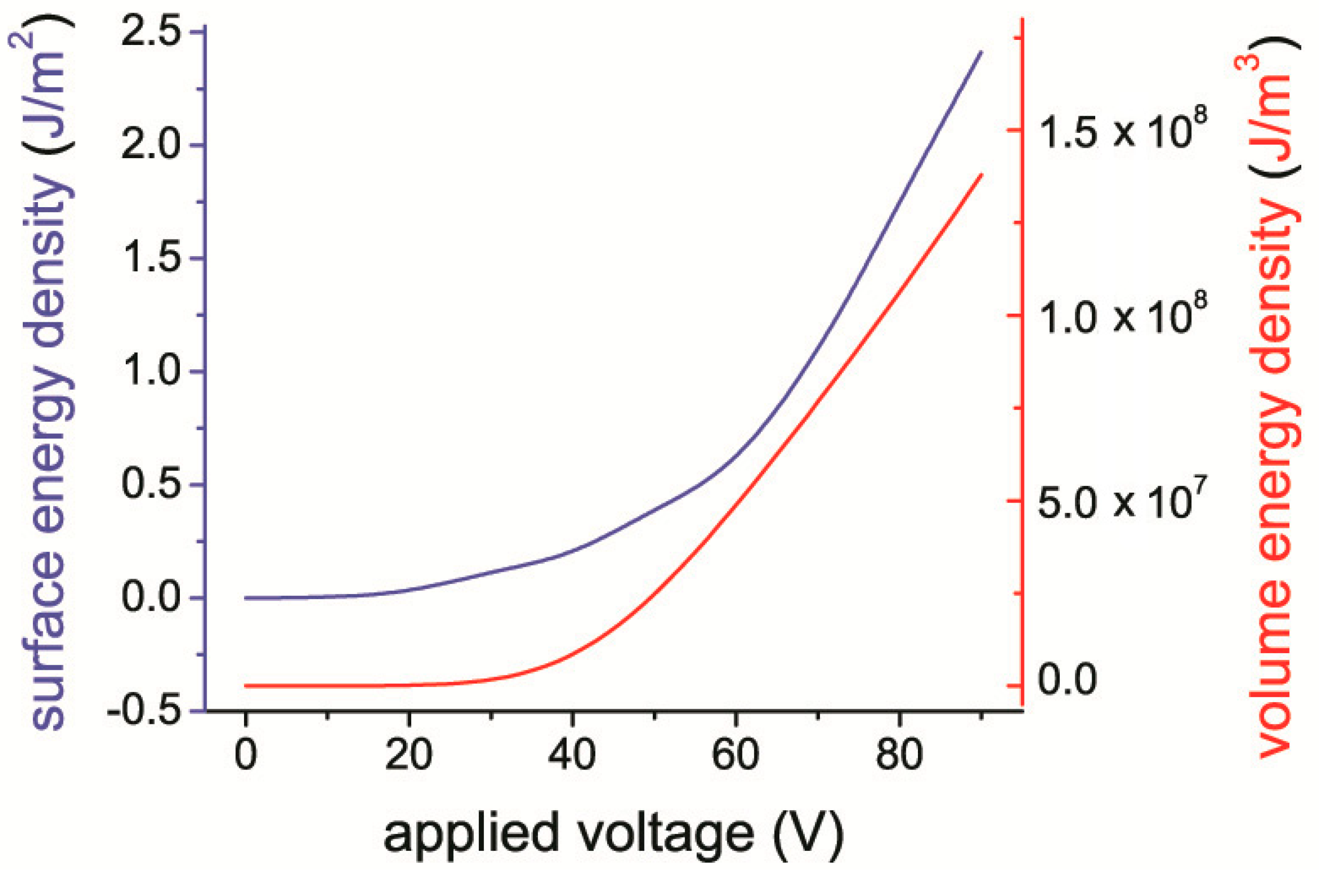
Based on the parameters indicated in Figure 5, it is possible to estimate the energy accumulated in the gap of the structure under consideration, for example, at a voltage of 90 V, see Figure 7. It is equal to 2.5 J/m2. Extrapolating the value of the total energy WS(V) to voltage equal to Vi = 330 V, and assuming that WS increases quadratically with increasing voltage, we get WS,max = 32 J/m2. Note that this is a lower estimate, since the dependence WS(V) is stronger than a quadratic one, because the gap decreases with increasing voltage.
We also have found experimentally that these micromotors reached an energy density of WS = 1 J/m2 with a V value of 50 V [19]. Assuming that this energy density with the rise of voltage increases proportionally to V2 and extrapolating this value to Vmax = 330 V, we get WS,max = 40 J/m2, which is two times less than the value of WS,max theoretically estimated above.
The value of the maximum power density, per unit weight of the structure, which can be reached for the described micromotors, is calculated as:
P m = W S , max f 0 h k ρ 1
where f0 is determined by Equation (17), ρ1 is the specific weight of the material of the substrates of stator and slider, h is the total thickness of the substrates, k is the surface filling ratio by metal petals. Taking k = 0.8, dP ≈ 1.5 μm, l = 100 μm, h = 1 mm and taking into account that the petals are made of beryllium bronze and the substrates are made of silicon, we get f0 ≈ 100 kHz and Pm = 4.3 × 10⁶ W/kg. This value of Pm exceeds the specific power of inductive engines by 3 orders of magnitude: the maximum value of Pm for high-speed inductive engines is 5 × 10³ W/kg, [30,31].
Estimates of the strength of the petals necessary to reach the limiting density of the converted energy WS,max = 80 J/m2, show that their thickness can be within 1.5–2 microns. Such thicknesses can be easily achieved technologically.
4. Discussion

1. It has been shown that the creation of MFGM structures based on thin films of ferroelectrics with high electric strength and with a large dielectric constant of more than 1000 makes it possible to achieve high values of electric fields in nanogaps between the surfaces of a moving electrode and a ferroelectric, up to 6 × 10¹⁰ V/m. The energy density in the nanogap of electromechanical transducers based on such structures reaches 1.6 × 10¹⁰ J/m3, which exceeds this parameter in known inductive and piezoelectric transducers by more than 4 orders of magnitude.
2. It has been shown that during electromechanical energy conversion in these structures, the maximum value of energy, up to 80 J/m2, is achieved by forming a gap 5 nm in width and using a voltage of 330 V and a ferroelectric film thickness of 4 μm.
3. The effects limiting the maximum energy density in these structures are impact ionization of the air in the gap and the breakdown of the structure. It has been established that in the vacuum mode, the mechanism limiting the increase in energy is the field evaporation of metal atoms from the surface of the moving electrode.

Author Contributions

Formal analysis, I.L.B. and E.G.K.; Investigation, I.L.B. and E.G.K.; Methodology, I.L.B. and E.G.K.; Project administration, Edward Gennadievich Kostsov; Writing – original draft, I.L.B. and E.G.K.; Writing – review & editing, E.G.K.

Funding

Work was carried out as part of the Comprehensive Program of Basic Research SB RAS “Interdisciplinary Integration Studies” for 2018 - 2020, project No. 273.

Conflicts of Interest

The authors declare no conflict of interest.

References

  1. Edminister, J.A. Schaum’s Outline of Theory and Problems of Ferromagnetics, 2nd ed.; McGraw-Hill: New York, NY, USA, 1995. [Google Scholar]
  2. Roundy, S.; Wright, P.K. A piezoelectric vibration based generator for wireless electronics. Smart Mater. Struct. 2004, 13, 1131–1142. [Google Scholar] [CrossRef] [Green Version]
  3. Bansal, R.K. A Textbook of Strength of Materials, 4th ed.; Laxmi Publications Ltd.: New Delhi, India, 2009. [Google Scholar]
  4. Sakane, Y.; Suzuki, Y.; Kasagi, N. The development of a high-performance perfluorinated polymer electret and its application to micro power generation. J. Micromech. Microeng. 2008, 18, 104011. [Google Scholar] [CrossRef]
  5. Ghalichechian, N.; Modafe, A.; Lang, J.H.; Ghodssi, R. Dynamic characterization of a linear electrostatic micromotor supported on microball bearings. Sens. Actuators. 2007, A136, 496–503. [Google Scholar] [CrossRef]
  6. Sarajlic, E.; Yamahata, C.; Cordero, M.; Fujita, H. An electrostatic 3-phase linear stepper motor fabricated by vertical trench isolation technology. J. Micromech. Microeng. 2009, 19, 074001. [Google Scholar] [CrossRef]
  7. Khan, F.U.; Qadir, M.U. State-of-the-art in vibration-based electrostatic energy harvesting. J. Micromech. Microeng. 2016, 26, 103001. [Google Scholar] [CrossRef]
  8. Xu, L.; Bu, T.Z.; Yang, X.D.; Zhang, C.; Wang, Z.L. Ultrahigh charge density realized by charge pumping at ambient conditions for triboelectric nanogenerators. Nano Energy 2018, 49, 625–633. [Google Scholar] [CrossRef]
  9. Hinchet, R.; Ghaffarinejad, A.; Lub, Y.; Hasani, J.Y.; Kima, S.-W.; Basset, P. Understanding and modeling of triboelectric-electret nanogenerator. Nano Energy 2018, 47, 401–409. [Google Scholar] [CrossRef]
  10. Hao, X. A review on the dielectric materials for high energy-storage application. J. Adv. Dielectr. 2013, 3, 1330001. [Google Scholar] [CrossRef]
  11. Baginskii, I.L.; Kostsov, E.G. Thin ferroelectric films as DRAM components. Russ. Microelectr. 1997, 26, 237–246. [Google Scholar]
  12. Babrauskas, V. Arc breakdown in air over very small gap distances. Fire Arson Investig 2015, 65, 40–46. [Google Scholar]
  13. Waliash, A.J.; Levit, L. Electrical breakdown and ESD phenomena for devices with nanometer-to-micron gaps. In Proceedings of the Reliability, Testing, and Characterization of MEMS/MOEMS II, San Jose, CA, USA, 25–31 January 2003; pp. 87–96. [Google Scholar]
  14. Schaffert, R.M. (Ed.) Electrophotography; John Wiley and Sons: Hoboken, NJ, USA, 1975; p. 517. [Google Scholar]
  15. Boyle, W.S.; Kisluk, P.; Germer, L.H. Electrical breakdown in high vacuum. J. Appl. Phys. 1955, 26, 720–725. [Google Scholar] [CrossRef]
  16. Meng, G.; Cheng, Y.; Chen, L.; Chen, Y.; Wu, K. Discharge behaviors of electrical breakdown across nanometer vacuum gaps. In Proceedings of the IEEE International Conference on Solid Dielectrics, Bologna, Italy, 30 June–4 July 2013; pp. 662–665. [Google Scholar]
  17. Meng, G.; Cheng, Y.; Wu, K.; Chen, L. Electrical characteristics of nanometer gaps in vacuum under direct voltage. IEEE Trans. Dielectrics Electrical Insulation 2014, 21, 1950–1956. [Google Scholar] [CrossRef]
  18. Krimmel, E.F.; Hezel, R. Si Silicon: Silicon Nitride in Microelectronics and Solar Cells; Springer Science & Business Media: Berlin, German, 1991. [Google Scholar]
  19. Baginsky, I.L.; Kostsov, E.G. High-energy capacitance electrostatic micromotors. J. Micromech. Microeng. 2003, 13, 190–200. [Google Scholar] [CrossRef]
  20. Muller, E.W. Field ionization and field ion microscopy. Adv. Electron. Electron Phys. 1960, 13, 83. [Google Scholar]
  21. Karahka, M.L. Physics in high electric fields. Ph.D. Thesis, Philosophy Dallhouse University, Halifax, NS, Canada, 2016. [Google Scholar]
  22. Baginsky, I.L.; Kostsov, E.G.; Sokolov, A.A. Electrostatic microgenerators of energy with a high specific power. Optoelectron. Instrum. Data Process. 2010, 46, 580–592. [Google Scholar] [CrossRef]
  23. Hasselkamp, D. Kinetic electron emission from solid surfaces under ion bombardment. In Particle Induced Electron Emission II; Hasselkamp, D., Rothard, H., Groeneveld, K.O., Kemmler, J., Varga, P., Winter, H., Eds.; Springer Tracts in Modern Physics, Springer Science & Business Media: Berlin, Germany, 1992; Volume 123, pp. 1–95. [Google Scholar]
  24. Baginsky, I.L.; Kostsov, E.G. Electrostatic micromotor based on the ferroelectric ceramics. J. Micromech. Microeng. 2004, 14, 1–7. [Google Scholar] [CrossRef]
  25. Kostsov, E.G. Ferroelectric-based electrostatic micromotors with nanometer gaps. IEEE Trans. Ultrasonics, Ferroelectr. Freq. Control 2006, 53, 2294–2298. [Google Scholar] [CrossRef] [PubMed]
  26. Baginsky, I.L.; Kostsov, E.G. MEMS based on thin ferroelectric layers. In Ferroelectrics – Applications; Intech Open L: London, UK, 2011; pp. 35–38. [Google Scholar]
  27. Baginsky, I.L.; Kostsov, E.G. Reversible high speed electrostatic contact. In Semiconductors; Pleiades Publishing, Ltd.: New York, NY, USA, 2010; Volume 44, pp. 1654–1657. [Google Scholar]
  28. Kostov, E.; Dyatlov, V.; Perlo, P. Electrostatic linear motor. European Patent N97830474.9-2207, 17 October 1996. [Google Scholar]
  29. Kostov, E.; Dyatlov, V.; Perlo, P. Step linear electrostatic motor. European Patent N97830473.1-2207, 17 October 1996. [Google Scholar]
  30. Xianchuan, L.; Yangyang, Z. Design of high energy density permanent magnet synchronous motor. In Proceedings of the 35th Chinese Control Conference, Chengdu, China, 27–29 July 2016; pp. 10232–10235. [Google Scholar]
  31. Siemens and Emrax claim best power to weight ratio for electric motors in the 5 to 10 kilowatt per kg range. Available online: https://www.nextbigfuture.com/2015/04/siemens-and-emrax-claim-best-power-to.html (accessed on 28 August 2019).
Figure 1. The dependence of the critical voltage on the size of the gap de at atmospheric air pressure: in metal-gap-metal structure (MGM) - (curve abcd) and metal-ferroelectric-gap-metal structures (MFGM) structures (mnbcd and kbcd curves). ecd is Paschen curve.
Micromachines 10 00746 g001
Figure 2. Equivalent circuit of the MFGM structure. Ri - leakage resistance of the insulator (ferroelectric).
Micromachines 10 00746 g002
Figure 3. Polarity effect in the process of moving electrode (ME) attraction to the surface of a ferroelectric film in the MFGM structure at application of voltage pulse with an amplitude of 50 V. 1: positive bias on ME, 2: negative.
Micromachines 10 00746 g003
Figure 4. Schematic of the structure metal (1) - gap (thickness de) - dielectric (BSN) (2) thickness dF - metal (3), (4) - substrate - silicon.
Micromachines 10 00746 g004
Figure 5. The change in the capacity of the MFGM structure and the size of the gap depending on the applied voltage (dF = 2.4 μm, ε = 3500).
Micromachines 10 00746 g005
Figure 6. A scheme illustrating for the motion effects for the petal micromotor. 1 – stator, consisted of ferroelectric film (5), deposited on silicon substrate (7) with metallic electrode sublayer (6), 2 – moving substrate (glass), 3 – petal (copper berillium), 4 – guides (schematically shown). A – initial state and position, t = 0; B – the state and position at the end of the first voltage pulse, t = tp, the moving substrate (slider) is shifted to h(t) and the petal is rolled to the length lr(t); C – the state and position, corresponding to the time t = T (T is the period of voltage pulses). The slider is shifted to the distance hΣ by inertia, a part of the petal lr is still attached to the ferroelectric surface; D – the state and position at the end of the second pulse, analogous to the view A, total shift is h + hΣ; E – the state and position, corresponding to the time t = 2T, analogous to the view C, toal shift is 2hΣ.
Micromachines 10 00746 g006
Figure 7. The energy density in the nanogap of the MFGM structure, depending on the applied voltage. (dF = 2.4 μm, ε = 3500).
Micromachines 10 00746 g007