
A Modulation Method for Three-Phase Dual-Active-Bridge Converters in Battery Charging Applications


Abstract
1. Introduction
2. Symmetric Duty-Cycle Modulation Method
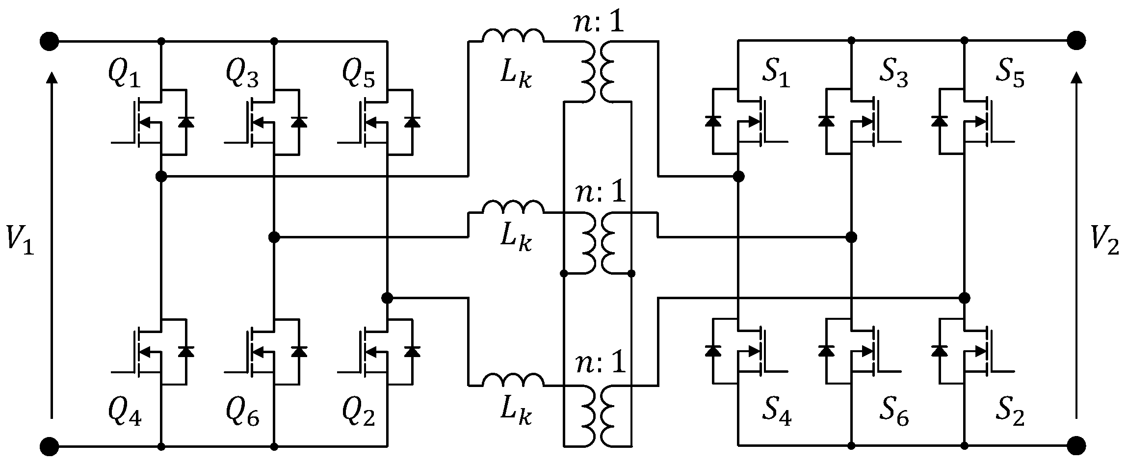
2.1. Three-Phase Dual-Active-Bridge Converters
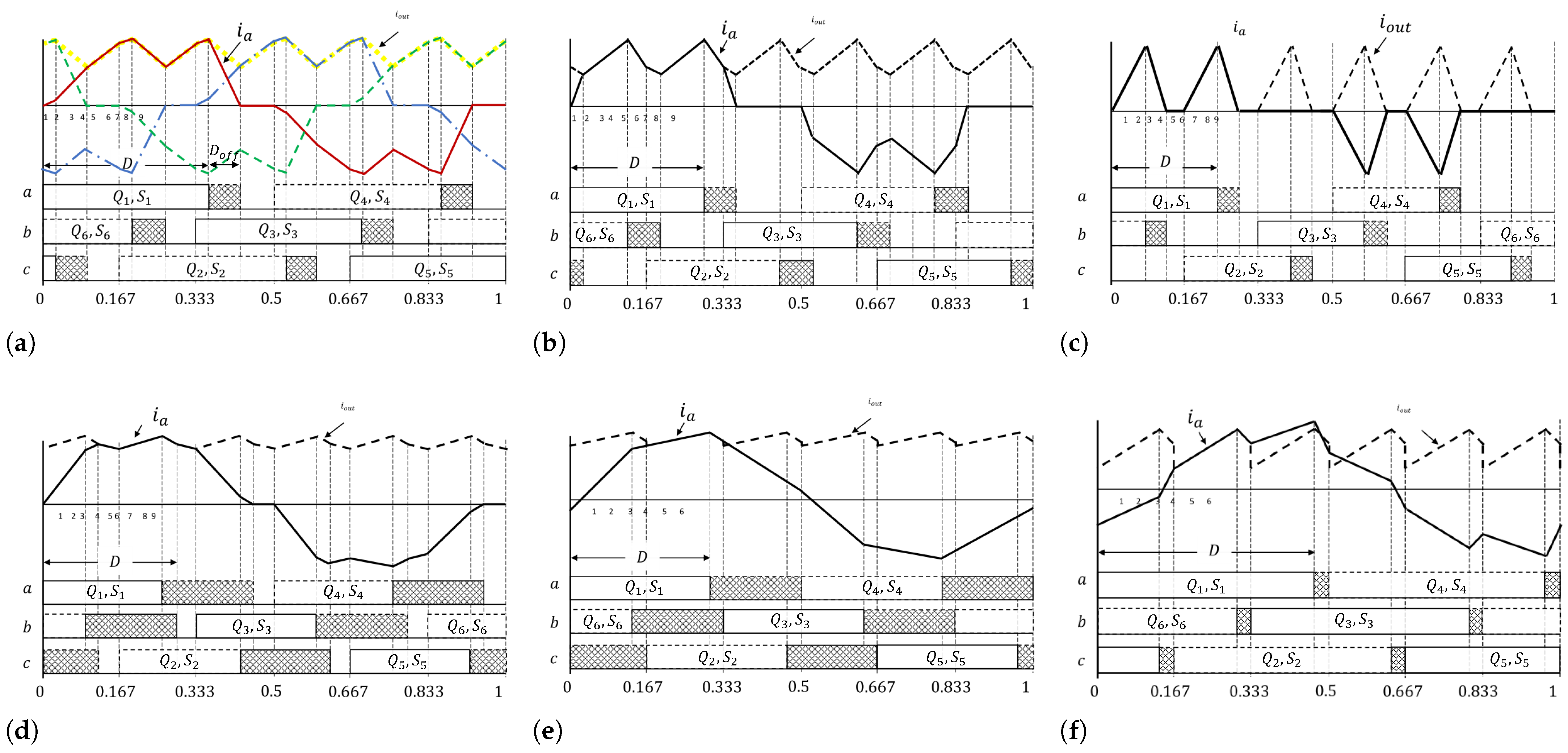
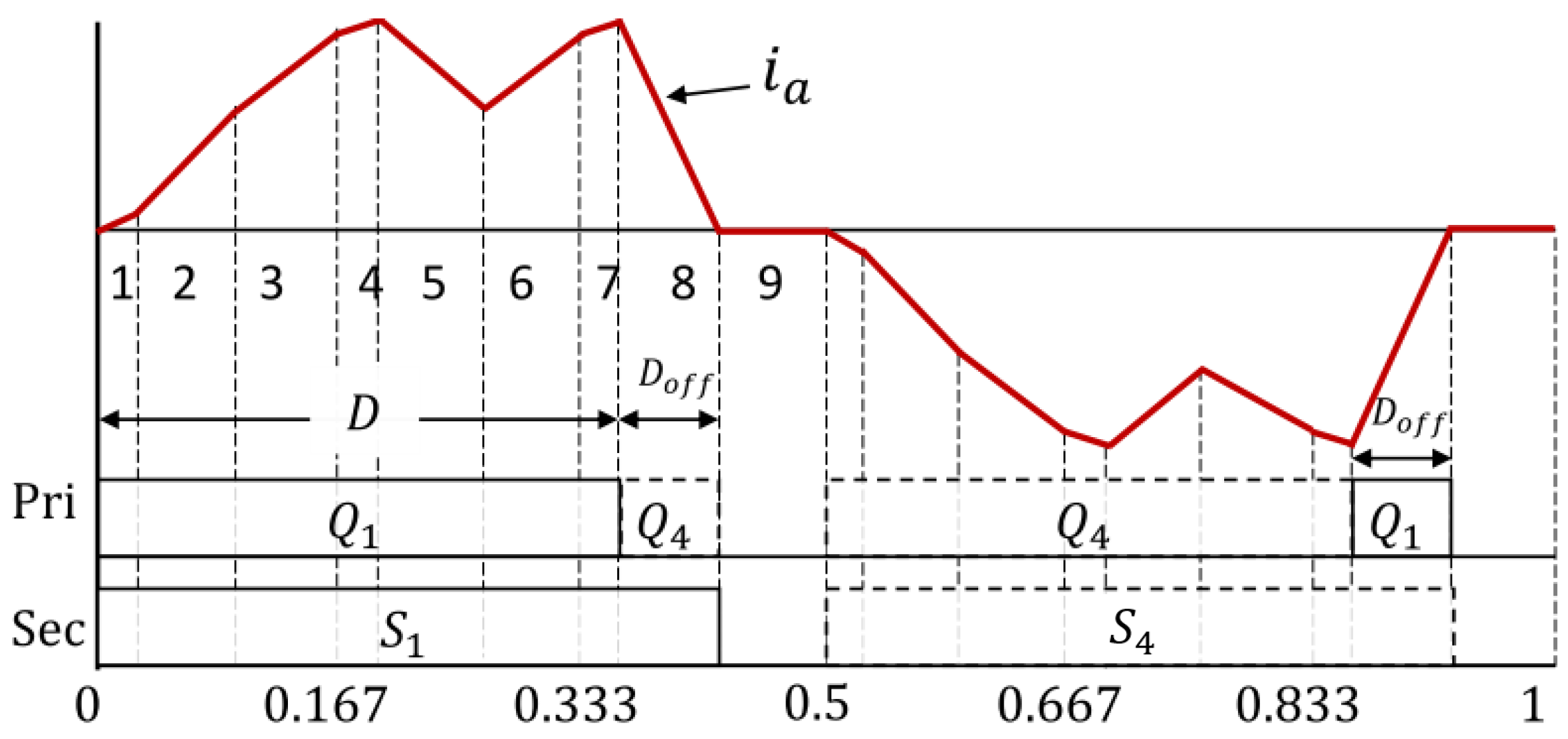
2.2. Steady-State Analysis of the Proposed SDM Method
2.2.1. State 2:
2.2.2. State 3:
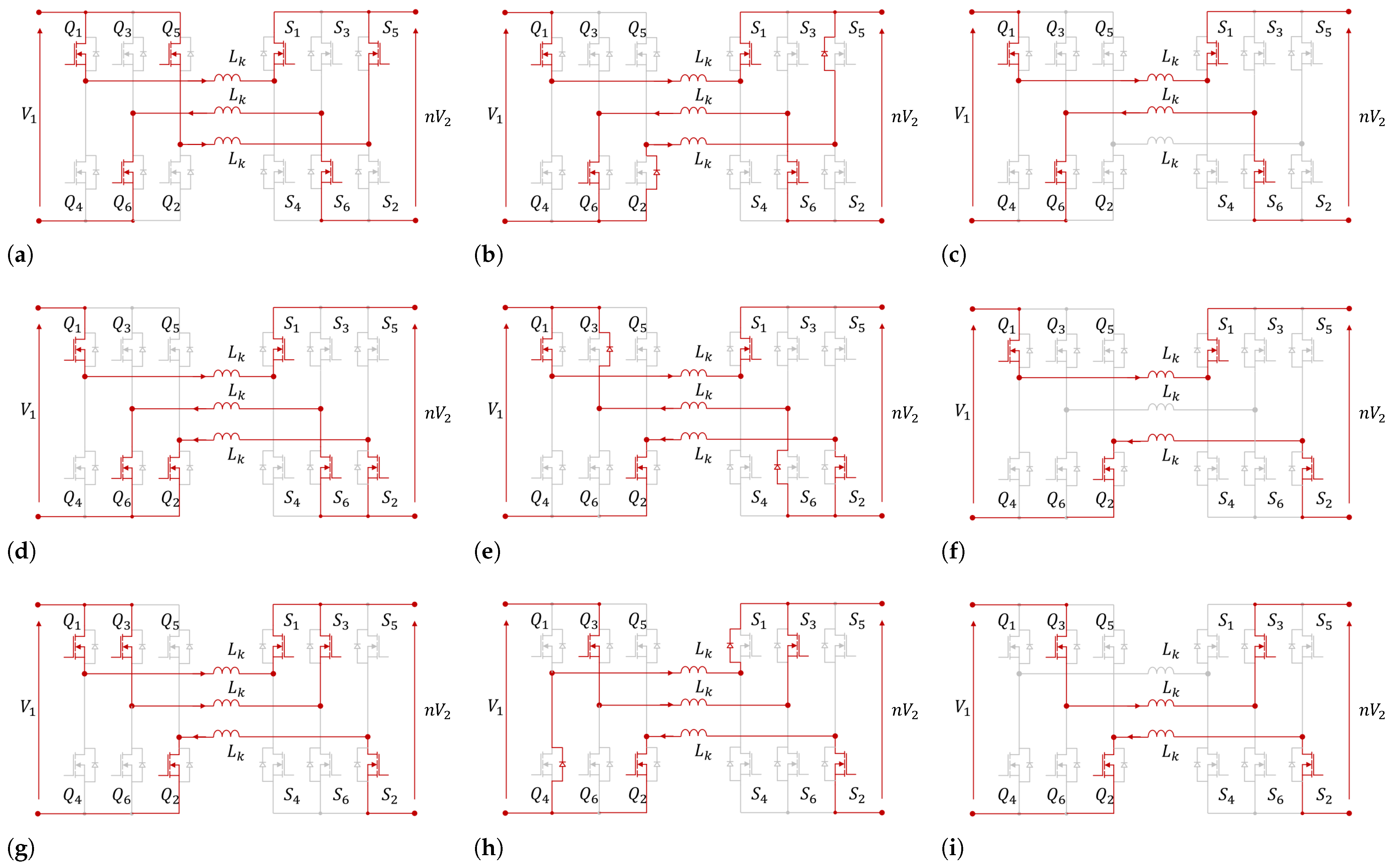
3. Comparison
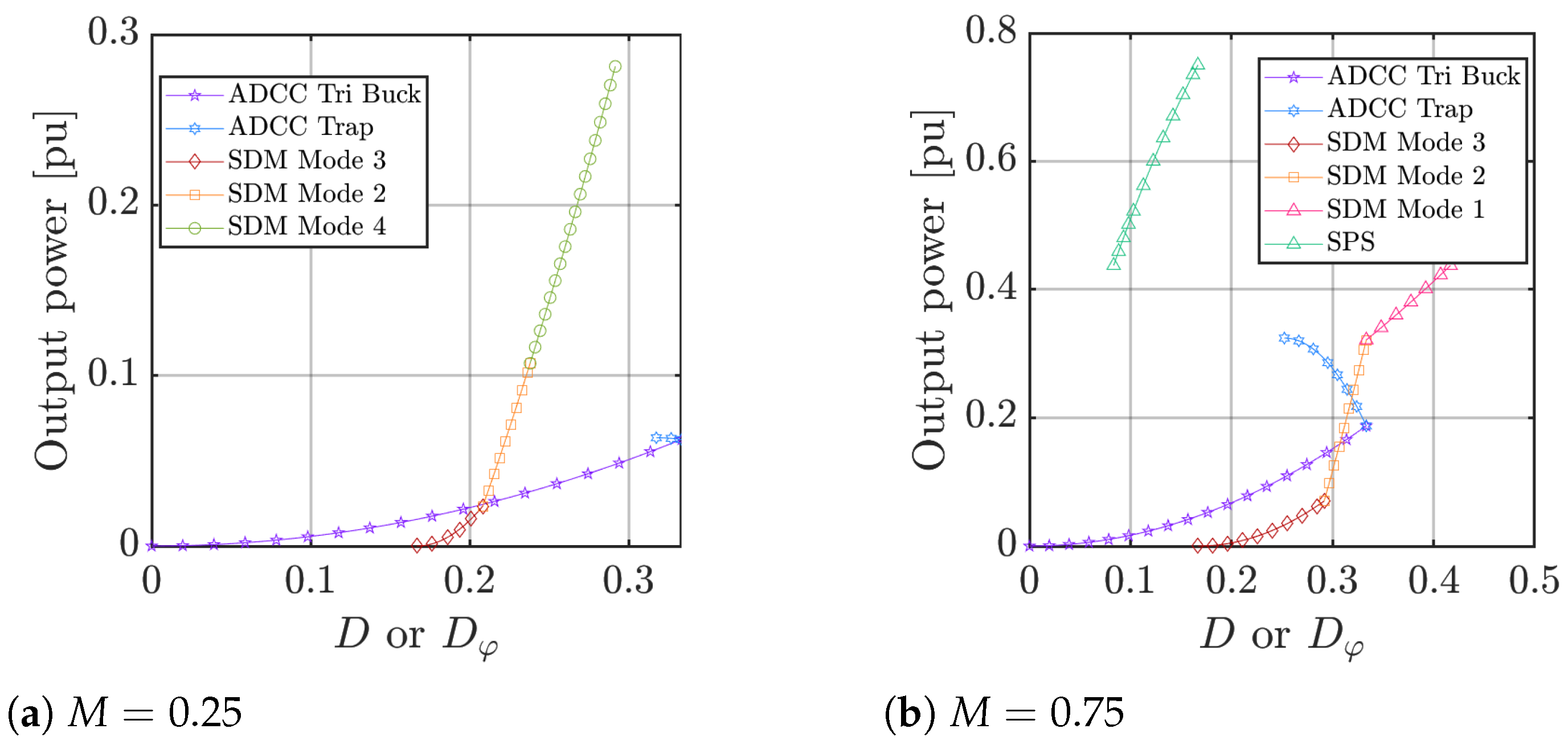
3.1. Soft-Switching Range
3.2. Power Flow with Mode Changing
3.3. Output Current Ripple
4. Diode Loss Elimination Technique
4.1. Proposed SDMM Technique
- i
- Precise determination of the present voltage gain M. The DC terminal voltages are sensed and from this, the voltage gain ratio M is calculated. A mismatch in determining M may lead to early or late turn-off of the corresponding switch that may reduce the effect of the proposed method.
- ii
- A high-resolution pulse-width modulation (PWM) module of the microcontroller. For instance, in this study, an STM32G474RE microcontroller from STMicroelectronics was used to generate the SDMM modulation pattern.
- iii
- Finally, the microcontroller with a floating-point unit (FPU). This is needed because the calculation of the diode conduction interval consists of some division and multiplication operations.
4.2. Loss Breakdown Analysis
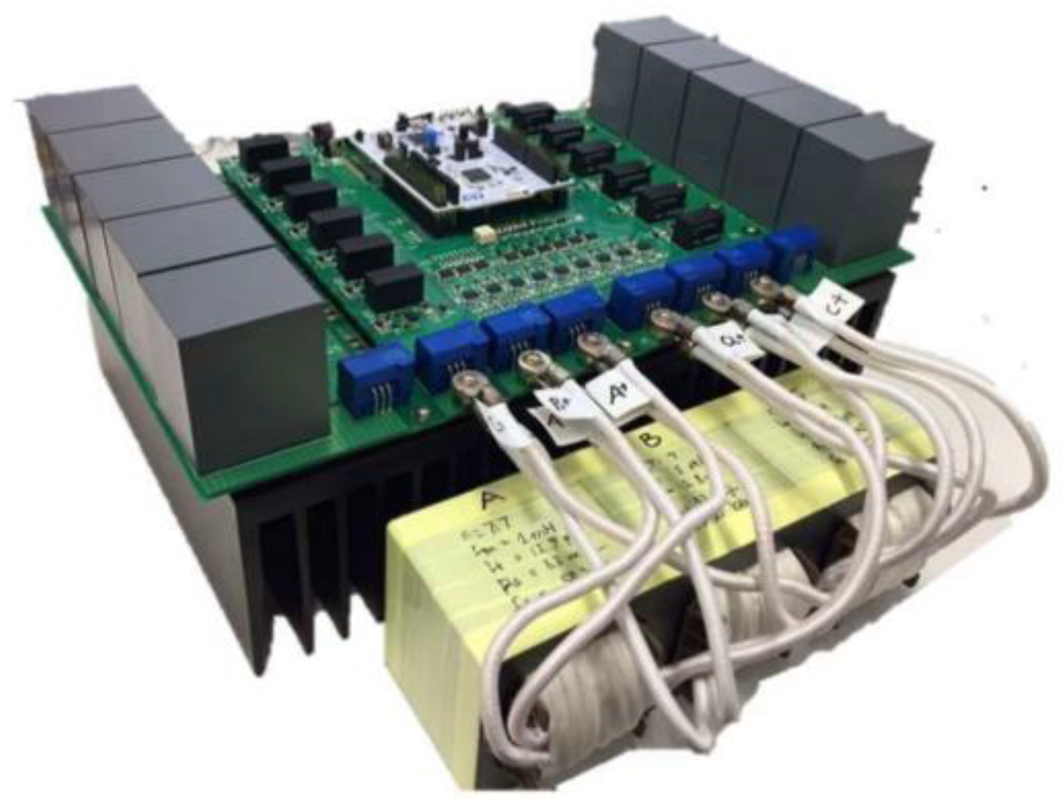
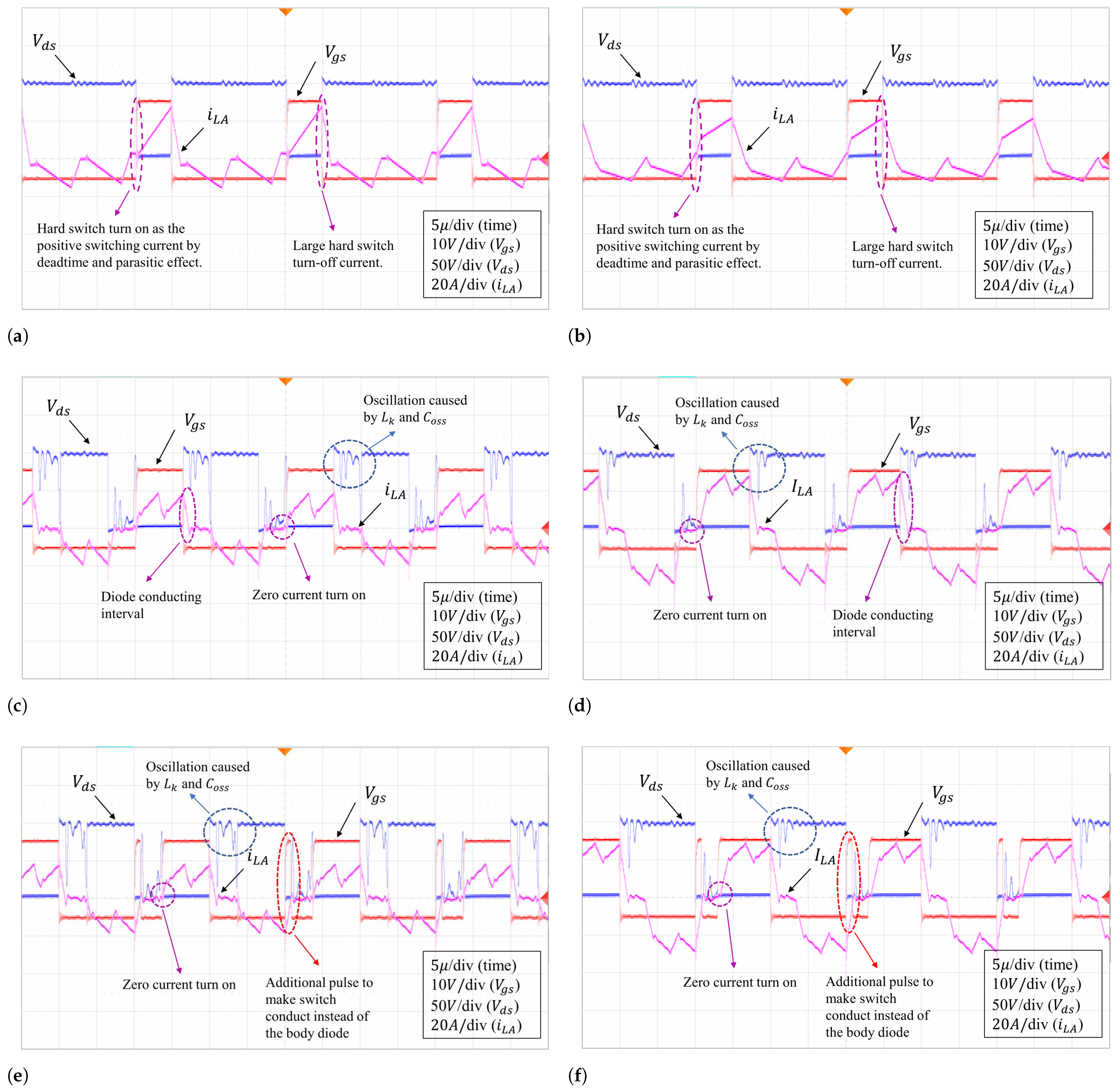
5. Experimental Results
6. Conclusions
Author Contributions
Funding
Institutional Review Board Statement
Informed Consent Statement
Data Availability Statement
Conflicts of Interest
References
- Kempton, W.; Tomić, J. Vehicle-to-grid power implementation: From stabilizing the grid to supporting large-scale renewable energy. J. Power Sources 2005, 144, 280–294. [Google Scholar] [CrossRef]
- Ota, Y.; Taniguchi, H.; Nakajima, T.; Liyanage, K.M.; Baba, J.; Yokoyama, A. Autonomous distributed V2G (vehicle-to-grid) satisfying scheduled charging. IEEE Trans. Smart Grid 2011, 3, 559–564. [Google Scholar] [CrossRef]
- Mouli, G.R.C.; Kaptein, J.; Bauer, P.; Zeman, M. Implementation of dynamic charging and V2G using Chademo and CCS/Combo DC charging standard. In Proceedings of the 2016 IEEE Transportation Electrification Conference and Expo (ITEC), Dearborn, MI, USA, 27–29 June 2016; pp. 1–6. [Google Scholar]
- Mouli, G.R.C.; Schijffelen, J.; van den Heuvel, M.; Kardolus, M.; Bauer, P. A 10 kW solar-powered bidirectional EV charger compatible with chademo and COMBO. IEEE Trans. Power Electron. 2018, 34, 1082–1098. [Google Scholar] [CrossRef]
- Inoue, S.; Akagi, H. A bidirectional DC–DC converter for an energy storage system with galvanic isolation. IEEE Trans. Power Electron. 2007, 22, 2299–2306. [Google Scholar] [CrossRef]
- Ting, P.; Shenghua, H.; Shuanghong, W. A three phase ZVS bidirectional DC-DC converter. In Proceedings of the 2008 IEEE Vehicle Power and Propulsion Conference, Harbin, China, 3–5 September 2008; pp. 1–6. [Google Scholar]
- De Doncker, R.W.; Divan, D.M.; Kheraluwala, M.H. A three-phase soft-switched high-power-density DC/DC converter for high-power applications. IEEE Trans. Ind. Appl. 1991, 27, 63–73. [Google Scholar] [CrossRef]
- Zhao, B.; Song, Q.; Liu, W.; Sun, Y. Overview of dual-active-bridge isolated bidirectional DC–DC converter for high-frequency-link power-conversion system. IEEE Trans. Power Electron. 2013, 29, 4091–4106. [Google Scholar] [CrossRef]
- He, P.; Khaligh, A. Comprehensive analyses and comparison of 1 kW isolated DC–DC converters for bidirectional EV charging systems. IEEE Trans. Transp. Electrif. 2016, 3, 147–156. [Google Scholar] [CrossRef]
- Haghbin, S.; Alatalo, M.; Yazdani, F.; Thiringer, T.; Karlsson, R. The design and construction of transformers for a 50 kW three-phase dual active bridge dc/dc converter. In Proceedings of the 2017 IEEE Vehicle Power and Propulsion Conference (VPPC), Belfort, France, 11–14 December 2017; pp. 1–5. [Google Scholar]
- Baars, N.H.; Everts, J.; Wijnands, C.G.; Lomonova, E.A. Performance evaluation of a three-phase dual active bridge DC–DC converter with different transformer winding configurations. IEEE Trans. Power Electron. 2015, 31, 6814–6823. [Google Scholar] [CrossRef]
- Zhang, J.; Wang, Z.; Shao, S. A three-phase modular multilevel DC–DC converter for power electronic transformer applications. IEEE J. Emerg. Sel. Top. Power Electron. 2016, 5, 140–150. [Google Scholar] [CrossRef]
- Segaran, D.; Holmes, D.G.; Mcgrath, B.P. Comparative analysis of single and three-phase dual active bridge bidirectional DC-DC converters. In Proceedings of the 2008 Australasian Universities Power Engineering Conference, Sydney, NSW, Australia, 14–17 December 2008; pp. 1–6. [Google Scholar]
- van Hoek, H.; Neubert, M.; Kroeber, A.; De Doncker, R.W. Comparison of a single-phase and a three-phase dual active bridge with low-voltage, high-current output. In Proceedings of the 2012 International Conference on Renewable Energy Research and Applications (ICRERA), Nagasaki, Japan, 11–14 November 2012; pp. 1–6. [Google Scholar]
- Chakraborty, S.; Vu, H.N.; Hasan, M.M.; Tran, D.D.; Baghdadi, M.E.; Hegazy, O. DC-DC converter topologies for electric vehicles, plug-in hybrid electric vehicles and fast charging stations: State of the art and future trends. Energies 2019, 12, 1569. [Google Scholar] [CrossRef]
- Wang, Y.C.; Ni, F.M.; Lee, T.L. Hybrid modulation of bidirectional three-phase dual-active-bridge DC converters for electric vehicles. Energies 2016, 9, 492. [Google Scholar] [CrossRef]
- Riedel, J.; Holmes, D.G.; McGrath, B.P.; Teixeira, C. ZVS soft switching boundaries for dual active bridge DC–DC converters using frequency domain analysis. IEEE Trans. Power Electron. 2016, 32, 3166–3179. [Google Scholar] [CrossRef]
- CHAdeMO Association. Technical Specifications of Quick Charger for Electric Vehicles; CHAdeMO 2.0; CHAdeMO Association: Paris, France, 2018; 84p. [Google Scholar]
- Chen, L.R.; Wu, S.L.; Shieh, D.T.; Chen, T.R. Sinusoidal-ripple-current charging strategy and optimal charging frequency study for Li-ion batteries. IEEE Trans. Ind. Electron. 2012, 60, 88–97. [Google Scholar] [CrossRef]
- Bessman, A.; Soares, R.; Vadivelu, S.; Wallmark, O.; Svens, P.; Ekström, H.; Lindbergh, G. Challenging sinusoidal ripple-current charging of lithium-ion batteries. IEEE Trans. Ind. Electron. 2017, 65, 4750–4757. [Google Scholar] [CrossRef]
- Uddin, K.; Moore, A.D.; Barai, A.; Marco, J. The effects of high frequency current ripple on electric vehicle battery performance. Appl. Energy 2016, 178, 142–154. [Google Scholar] [CrossRef]
- Zhao, B.; Yu, Q.; Sun, W. Extended-phase-shift control of isolated bidirectional DC–DC converter for power distribution in microgrid. IEEE Trans. Power Electron. 2011, 27, 4667–4680. [Google Scholar] [CrossRef]
- Shi, H.; Wen, H.; Chen, J.; Hu, Y.; Jiang, L.; Chen, G.; Ma, J. Minimum-backflow-power scheme of DAB-based solid-state transformer with extended-phase-shift control. IEEE Trans. Ind. Appl. 2018, 54, 3483–3496. [Google Scholar] [CrossRef]
- Zhao, B.; Song, Q.; Liu, W. Efficiency characterization and optimization of isolated bidirectional DC–DC converter based on dual-phase-shift control for DC distribution application. IEEE Trans. Power Electron. 2012, 28, 1711–1727. [Google Scholar] [CrossRef]
- Krismer, F.; Kolar, J.W. Closed form solution for minimum conduction loss modulation of DAB converters. IEEE Trans. Power Electron. 2011, 27, 174–188. [Google Scholar] [CrossRef]
- van Hoek, H.; Neubert, M.; De Doncker, R.W. Enhanced modulation strategy for a three-phase dual active bridge–Boosting efficiency of an electric vehicle converter. IEEE Trans. Power Electron. 2013, 28, 5499–5507. [Google Scholar] [CrossRef]
- Hu, J.; Soltau, N.; De Doncker, R.W. Asymmetrical duty-cycle control of three-phase dual-active bridge converter for soft-switching range extension. In Proceedings of the 2016 IEEE Energy Conversion Congress and Exposition (ECCE), Milwaukee, WI, USA, 18–22 September 2016; pp. 1–8. [Google Scholar]
- Hu, J.; Yang, Z.; Soltau, N.; De Doncker, R.W. A duty-cycle control method to ensure soft-switching operation of a high-power three-phase dual-active bridge converter. In Proceedings of the 2017 IEEE 3rd International Future Energy Electronics Conference and ECCE Asia (IFEEC 2017-ECCE Asia), Kaohsiung, Taiwan, 3–7 June 2017; pp. 866–871. [Google Scholar]
- Huang, J.; Li, Z.; Shi, L.; Wang, Y.; Zhu, J. Optimized modulation and dynamic control of a three-phase dual active bridge converter with variable duty cycles. IEEE Trans. Power Electron. 2018, 34, 2856–2873. [Google Scholar] [CrossRef]
- Jiang, H.; Wei, J.; Dai, X.; Zheng, C.; Ke, M.; Deng, X.; Sharma, Y.; Deviny, I.; Mawby, P. SiC MOSFET with built-in SBD for reduction of reverse recovery charge and switching loss in 10-kV applications. In Proceedings of the 2017 29th International Symposium on Power Semiconductor Devices and IC’s (ISPSD), Sapporo, Japan, 28 May–1 June 2017; pp. 49–52. [Google Scholar]
- Sung, W.; Baliga, B.J. On developing one-chip integration of 1.2 kV SiC MOSFET and JBS diode (JBSFET). IEEE Trans. Ind. Electron. 2017, 64, 8206–8212. [Google Scholar] [CrossRef]
- Sung, W.; Baliga, B.J. Monolithically integrated 4H-SiC MOSFET and JBS diode (JBSFET) using a single ohmic/Schottky process scheme. IEEE Electron Device Lett. 2016, 37, 1605–1608. [Google Scholar] [CrossRef]
- Nguyen, D.D.; Yuktta, K.; Katou, A.; Yoshida, S. A comparison study of modulation methods for three-phase dual-active-bridge converters in battery charging applications. In Proceedings of the 2021 IEEE 12th Energy Conversion Congress & Exposition-Asia (ECCE-Asia), Singapore, 24–27 May 2021; pp. 1033–1038. [Google Scholar]
- Nguyen, D.D.; Yukita, K.; Katou, A.; Yoshida, S. A new method to extend the soft-switching area of three-phase dual-active-bridge converters. In Proceedings of the 2021 IEEE 12th Energy Conversion Congress & Exposition-Asia (ECCE-Asia), Singapore, 24–27 May 2021; pp. 736–742. [Google Scholar]
- Nguyen, D.D.; Bui, N.T.; Yukita, K. Design and optimization of three-phase dual-active-bridge converters for electric vehicle charging stations. Energies 2019, 13, 150. [Google Scholar] [CrossRef]
- Hu, J.; Yang, Z.; Cui, S.; De Doncker, R.W. Closed-form asymmetrical duty-cycle control to extend the soft-switching range of three-phase dual-active-bridge converters. IEEE Trans. Power Electron. 2021, 36, 9609–9622. [Google Scholar] [CrossRef]
- McLyman, C.W.T. Transformer and Inductor Design Handbook; CRC Press: Boca Raton, FL, USA, 2004. [Google Scholar]


| Mode 1: | |
| Mode 2: | |
| Mode 3: | |
| Mode 4: | |
| Mode 5: | |
| Mode 6: |
| Parameters | Symbol | Value |
|---|---|---|
| Input voltage | 100 V | |
| Output voltage | 60–100 V | |
| Scale down power | 2 kW | |
| Frequency | 50 kHz | |
| Turn ratio | n | 1 |
| Leakage inductance | 12.5 H | |
| Wire | Lizt 1650AWG38 | |
| Core | EE42/21/15 (N87) | |
| SiC MOSFET | CREE C2M0025120D |
Disclaimer/Publisher’s Note: The statements, opinions and data contained in all publications are solely those of the individual author(s) and contributor(s) and not of MDPI and/or the editor(s). MDPI and/or the editor(s) disclaim responsibility for any injury to people or property resulting from any ideas, methods, instructions or products referred to in the content. |
© 2023 by the authors. Licensee MDPI, Basel, Switzerland. This article is an open access article distributed under the terms and conditions of the Creative Commons Attribution (CC BY) license (https://creativecommons.org/licenses/by/4.0/).
Share and Cite
Nguyen, D.-D.; Pham, T.-T.; Le, T.-T.; Choi, S.; Yukita, K. A Modulation Method for Three-Phase Dual-Active-Bridge Converters in Battery Charging Applications. Sustainability 2023, 15, 5170. https://doi.org/10.3390/su15065170
Nguyen D-D, Pham T-T, Le T-T, Choi S, Yukita K. A Modulation Method for Three-Phase Dual-Active-Bridge Converters in Battery Charging Applications. Sustainability. 2023; 15(6):5170. https://doi.org/10.3390/su15065170
Chicago/Turabian StyleNguyen, Duy-Dinh, The-Tiep Pham, Tat-Thang Le, Sewan Choi, and Kazuto Yukita. 2023. "A Modulation Method for Three-Phase Dual-Active-Bridge Converters in Battery Charging Applications" Sustainability 15, no. 6: 5170. https://doi.org/10.3390/su15065170
APA StyleNguyen, D.-D., Pham, T.-T., Le, T.-T., Choi, S., & Yukita, K. (2023). A Modulation Method for Three-Phase Dual-Active-Bridge Converters in Battery Charging Applications. Sustainability, 15(6), 5170. https://doi.org/10.3390/su15065170