1. Introduction
With the passage of time, LED lights have become a more advanced lighting source as compared to incandescent and CFL lamps due to more efficient and good color rendering. Even LEDs are the most efficient source of light to date [
1]. Since Thomas Edison produced the first incandescent lamp in 1879, electrical lighting has been a significant technology. As the next generation of light sources, LEDs have been the focus of research as environmental and energy conservation concerns grow. Compared to fluorescent tubes and incandescent light bulbs, LEDs are significantly more energy efficient with steady growth in luminous efficiencies [
2,
3]. Replacing traditional lamps with LEDs would result in significant CO
2 reductions and eliminate mercury waste from disposal [
4,
5].
High-bright white LEDs have recently attracted the attention of the consumer in industrial applications, particularly in street lighting. Street lighting improves security and safety in individual residences, utility companies, and cities. LEDs are not fully resistive loads like incandescent bulbs and thus must cope with power factor correction and total harmonic distortion [
6]. LEDs do not have tubes or filaments, making them incredibly durable and capable of operating with the driver for longer periods. An AC-DC converter must be utilized to power LED street lighting systems from the input voltage of alternating current. As a result, designing LED drivers is critical to designing a system with high energy efficiency and superior PF and THD performance. Switch-mode LED drivers are very common due to their ability to convert power at high frequencies due to their switching-type architecture [
7].
2. Literature Review
Single-stage [
8,
9], two-stage [
10,
11], and integrated LED driver systems [
12,
13] are the three different types of LED driver systems. The single-stage LED driver, an AC/DC converter, delivers a constant output current for the LED and unity power factor. A DC/DC converter and an AC/DC power factor correction converter make up the two stages of the two-stage system. Certainly, integrated topologies have lately been introduced to reduce the price and size. As an example, single-stage and integrated systems have some advantages due to the single energy conversion, such as high efficiency and minimal design costs. However, the power factor correction of these topologies leads to a significant output voltage ripple because of the absence of electrolytic capacitors. The ripple in the low-frequency current causes LEDs to flicker. These integrated solutions and single-stage are employed for LED replacement bulbs rather than LED street lighting systems when small-size converters are necessary. Existing PFC-based two-stage converters have a power factor of unity, but they are not economically viable. As a result, single-stage techniques for increasing system dependability have been created by combining the DC-DC converter and PFC circuit. Single-stage converters can save prices, but they haven’t been very successful because of a number of problems. The converters proposed in [
14,
15] have a low power conversion efficiency while having a bulk capacitor of lower voltage and high PF. The converter in [
16] had a complicated control circuit to maintain a 400-V bus voltage and only improved efficiency in low-power conditions. The THD was significant when the input voltage was increased in [
17], and the voltage exceeded 600 volts across the switches. Hard switching is frequently the outcome, which reduces system efficiency and increases power losses.
LLC resonant circuits with soft-switching characteristics [
18,
19] and half-bridge-based DCM single-stage PFC converters were used to increase system efficiency [
20]. The converters, on the contrary, operated with low input voltage and a bus voltage more than twice as high as the maximum input voltage. For the applications of high-input voltage, converters must use an inexpensive and large storage capacitor with a high-rated voltage. In [
21], a single-stage PFC converter with an LLC resonant circuit based on half-bridge and DCM interleaving boost circuits had a lower bus voltage that was somewhat greater than the maximum input voltage. As a result, the converter can handle large input voltages. ZCS at secondary-side diodes and ZVS at primary-side switches were used to reduce system switching loss. The topology was further enhanced using a single boost inductor instead of two boost inductors [
22]. In BCM mode, interleaving boost circuits shared a boost inductor to achieve the power factor correction function. An electrolytic capacitor is used in the converter because the estimated life span of the converter is shorter than that of the LEDs.
In [
23], a single-stage LED street light driver was proposed that integrates a half-bridge-type series-resonant converter, a bridge rectifier, and an interleaved boost PFC converter. The level of DC-bus voltage is increased, and two DC-linked capacitors are required due to the high voltage stresses of power switches that took place in this version due to the boost-type power conversion. Another single-stage street light driver based on interleaved boost converter is presented in [
24]. It can operate at utility-line voltages of 100–120 V in American and Asian countries, but due to boost-type power conversion, it can also operate at higher utility-line voltages of 220–240 V in European countries. In addition, in this version, the power switches will experience higher voltage stresses.
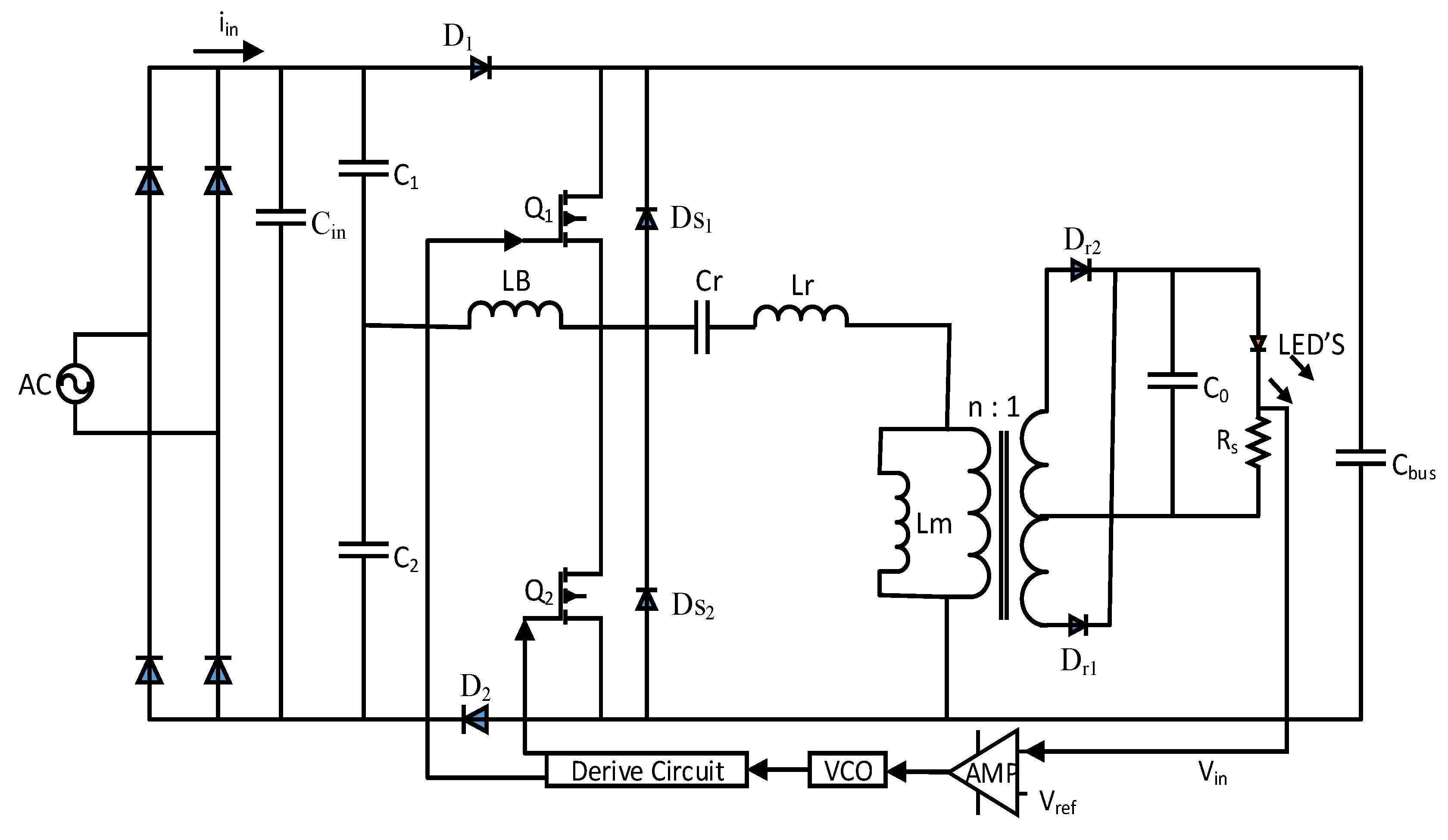
To meet these challenges, this article offers a design for a single-stage power factor corrected AC-DC converter which is appropriate for working at high utility-line voltages along with decreased voltage levels on the DC-linked capacitor and reduced voltage stresses on the power switches due to buck-boost-type power conversion. The authors in [
22] originally introduced the improvised architecture as shown in
Figure 1. This work is improved by running high-voltage LEDs in two strings with equal currents using a double half-wave rectifier on the secondary side. The converter removes one filter capacitor on the side of the DC input. The smooth switching characteristics of the LLC resonant circuit minimize the power losses of the switches. A metalized polypropylene capacitor was used, which significantly lowered the bus voltage capacitance. On the output side, small filter capacitors are utilized. Because of the decreased capacitance, the electrolytic capacitor is more likely to be removed, increasing the potential driver lifetime. The commercial resonant controller IC L6598 controls the half-bridge power switches for the driver, greatly reducing costs.
3. Structure of the Circuit
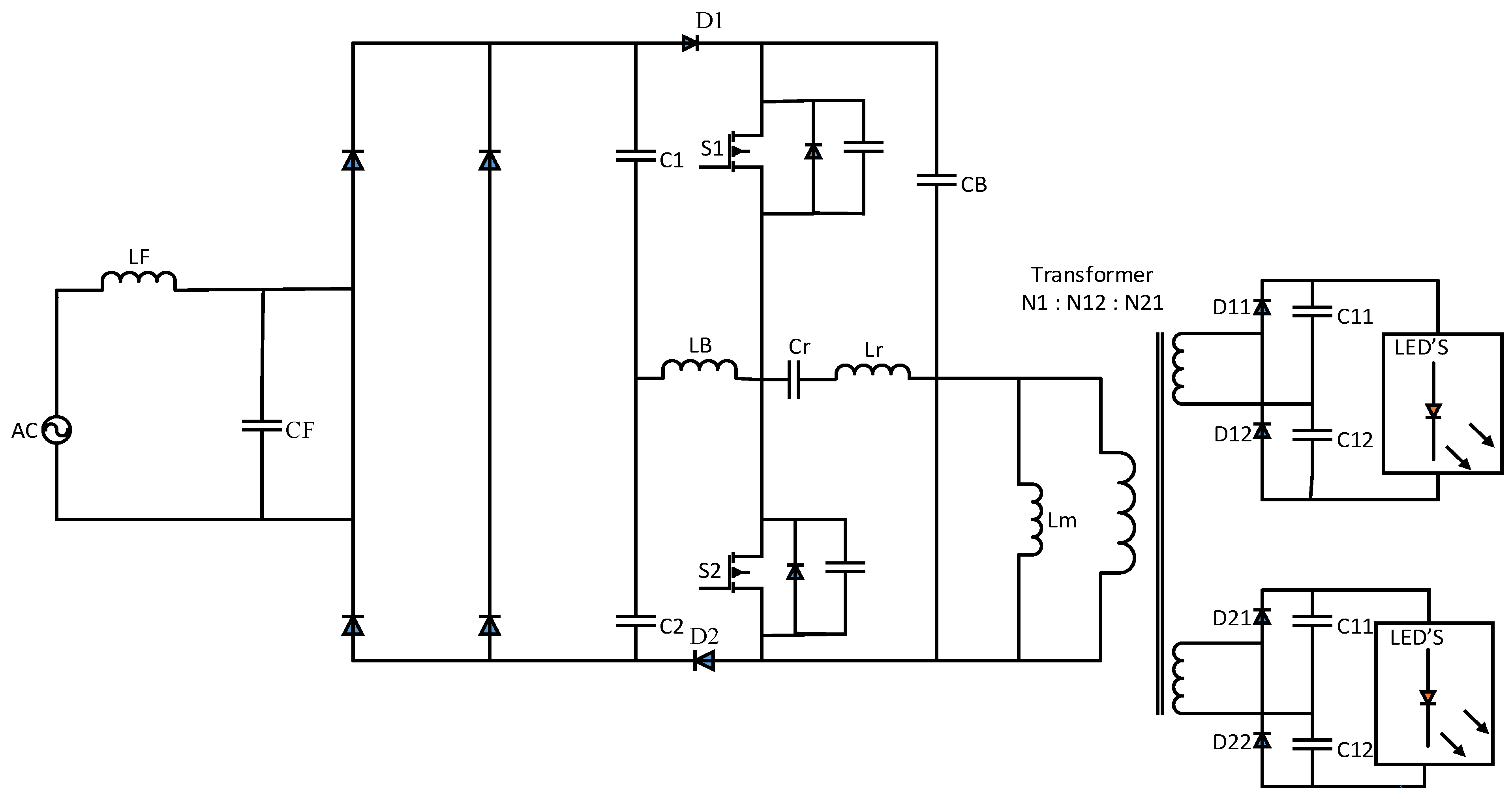
Figure 2 shows the desired LED driver’s design. The prosed LED driver contains a full-bridge rectifier that converts the AC input supply into a DC supply, C1, and C2 are two voltage dividing capacitors, D1 and D2 are two ultrafast boost diodes, LB is an inductor that is shared by both boost converters, two power MOSFETs S1 and S2, the Cs1 and Cs2, and Ds1 and Ds2 are the parasitic capacitors and diodes of switches and power switches respectively. DC bus capacitors C
bus, LLC resonant tank, Cr, Lr and L
M are resonant capacitors, resonant inductor and magnetizing inductor, a transformer which has one primary and two independent and identical secondary windings, two output rectifier diodes of first secondary winding D11 and D12, and output capacitors of first secondary winding C11 and C12. Two output rectifier diodes of 2nd secondary winding D21 and D22 and output capacitors of 2nd secondary winding C21 and C22. We can obtain two boost converters by combining the half-bridge LLC converter switches S1 and S2. The first boost circuit is formed by switch S1, diode D1, boost inductor LB, bus capacitor Cbus, and diode Ds2. The 2nd boost converter is formed by switch S
2, diode D2, boost inductor L
B, bus capacitor C
bus, and diode Ds
1. Both converters share the boost inductor and bus capacitor, which reduces their size. Both boost converters operate in BCM (boundary conduction mode) with an almost 50% duty cycle. And both switches are turned on with ZVS, and diodes of the secondary side are turned on and off with ZCV, which reduces switching losses and increases its efficiency.
The proposed topology consists of five major parts: bridge rectifier, two BCM boost converters, switching network, LLC resonant tank, and voltage doubler rectifier. The 1st part consists of a bridge rectifier that converts the AC power into DC because LEDs require DC current for their operation. If we want to drive LED lights from AC means, then the AC-DC conversion stage is necessary. The 2nd part consists of BCM boost converters that share the inductor LB and buss capacitor Cbus operation in BCM (boundary conduction mode), providing natural power factor correction. The 3rd part is the switching network; the output of this network is a square wave supplied to the tank circuit. The fourth part is the half LLC resonant converter which takes a square wave at the input and produces pure sinusoidal resonance frequency oscillations; a square wave is provided by the third part of the proposed circuit, which is the half-bridge inverter. Then the power is transferred to the transformer’s secondary windings, which are connected with voltage doubler rectifiers that convert the AC power into DC and are supplied to the LEDs. Light is emitted from LEDs in the form of photons, as shown by the arrows along the LEDs.
Proposed Converter with Coupled Inductor
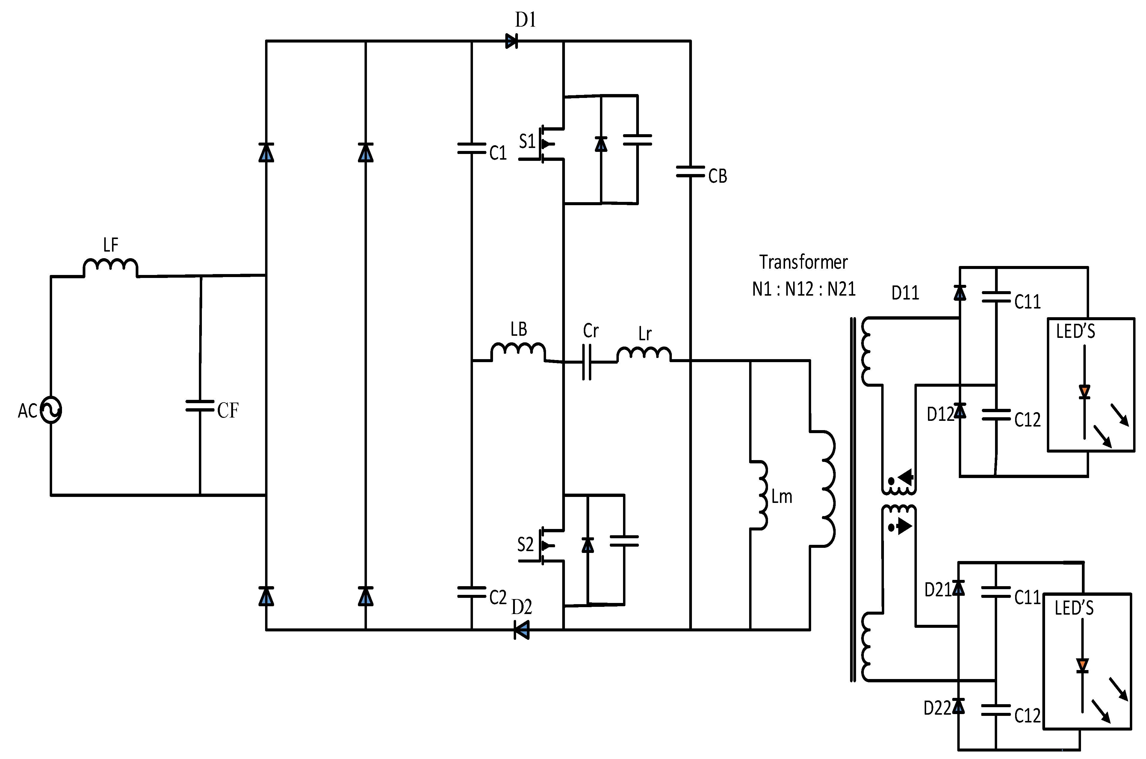
To encounter the magnetic coupling issue, a coupled inductor is added on the secondary side proposed converter with coupled inductor on the secondary side as shown in
Figure 3.
The proposed design, as shown in
Figure 3, is a two-channel LED driver that is built on the integration of two BCM boost converters and a half-bridge LLC converter with the design of the boost inductor Lb in such a way that both converters operate in boundary conduction mode; in one switching cycle, the current in the boost inductor hits a positive maximum, a negative maximum, and then returns to zero. Both switches are operated with approximately 50% duty cycle. The purpose of the first stage is PCF, and 2nd stage (integrated with the first stage) is the power control stage which provides the appropriate voltages and current to the LEDs with high efficiency. Then LLC resonant converter regulates the power flow. The LLC tank circuit takes square waves as input, performs wave shaping (converts into sinusoidal oscillations), and provides the ZVS of MOSFETs on the primary side. Power is transferred to the converter’s secondary windings, where it is rectified (converted into DC) with the help of a voltage double rectifier; the proposed system has two independent secondary windings means two independent LEDs strings are attached on the secondaries of the transformer with the equal load. If one LED string is shorted, the other will work properly; also, using two strings reduces the voltage stresses on secondary side diodes. The driver has low bus voltage compared to the conventional topologies of LED drivers; this reduces the voltage stresses on the switches. Film capacitors are used instead of the proposed electrolytic capacitor system. If the switch operated under normal operating conditions, the component’s life is even more than that of the datasheet’s lifetime.
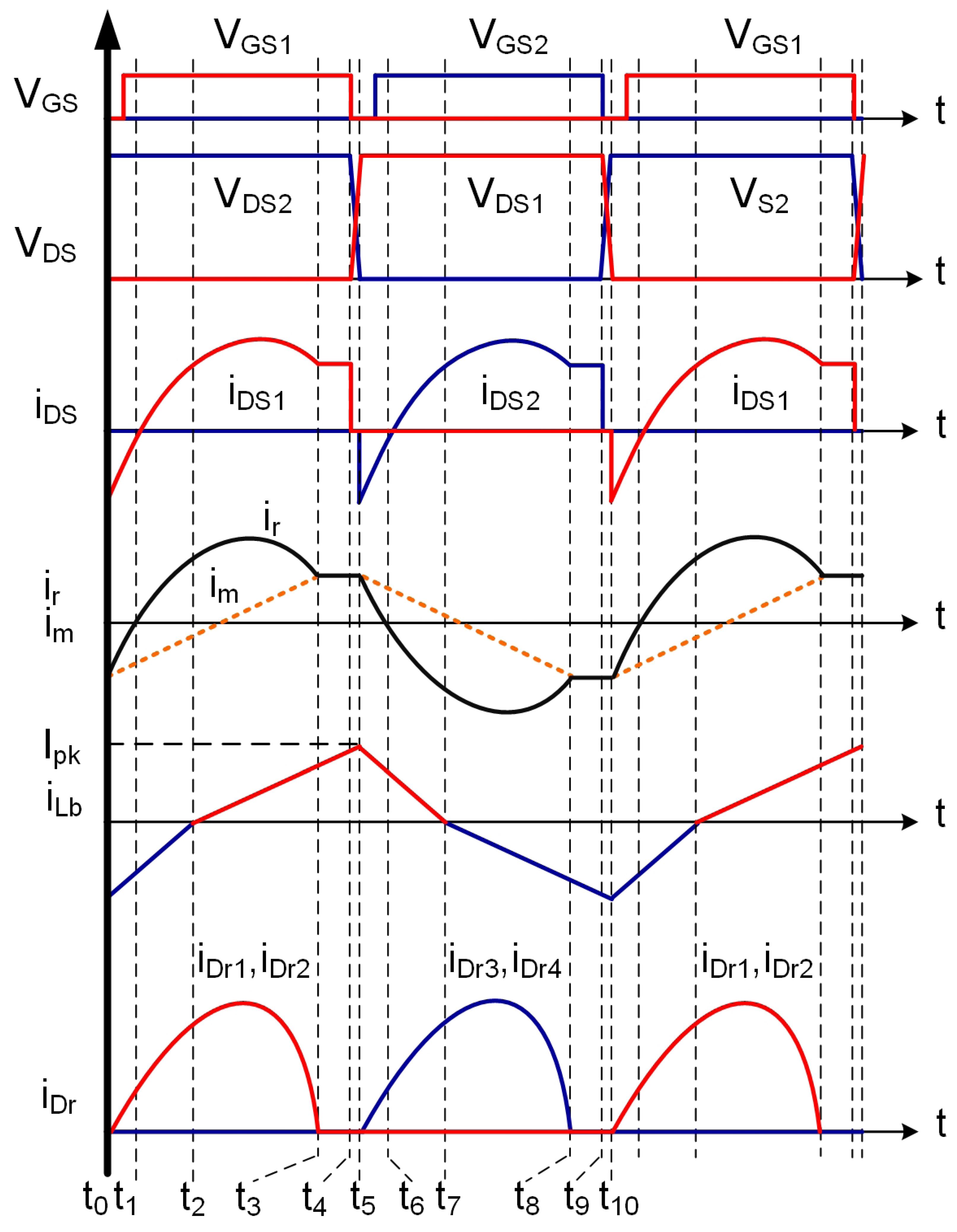
The steady-state working waveforms of the converter are presented in
Figure 4. From the waveforms, it can be seen that the boost inductor L
b functions in BCM and that the current
peaks twice during a switching period. Here, the boost inductor L
b is alternately charged and discharged by each of the two boost circuits.
The switches are turned on with ZVS after the drain-source voltages reduce to zero and their parasitic capacitors are discharged. As a result, the turn-on-switching losses are greatly reduced. The drain-source voltages increase as the switches’ parasitic capacitors charge in the meanwhile. Here, the capacitive loss is removed, allowing for the erasure of the turn-off switching losses as well. The switches repeatedly go through this intermittent on-off cycle.
4. Gain Analysis of the Proposed Converter
A half-bridge LLC resonant DC-DC converter’s gain characteristics are examined using the first harmonic approximation approach (FHA). Let
be the fundamental component of the input voltage of the tank circuit, and
is the switching frequency.
For the fundamental component value of n = 1.
The secondary current of the transformer or input current of the voltage doubler rectifier, which has a peak, can be calculated as:
By applying Fundamental Harmonic Approximation, the
RMS secondary voltages of the transformer can be calculated as:
As mentioned above, due to the voltage doubler rectifier, the secondary voltages of the transformer are half of the output voltages.
To calculate the RMS value of the secondary voltages, Equation (6) is divided by
.
Ac resistance (
) of voltage doubler rectifier be found as:
To simplify the analysis, secondary side resistance (
Rac) can be referred to as the primary side.
The voltage across the
is equal to the primary side voltage of the transformer, which can be calculated as
Generalized expiration of voltage gain ‘M’ and its DC gain G
dc of half-bridge LLC resonant converter with voltage doubler rectifier can be calculated from Equation (11).
where
is the proposed converter output voltage,
represents DC bus Voltage, Q is the quality factor, A is the ratio of magnetizing inductance to resonant inductance,
is AC load resistance, n is transformer’s turn ratio,
normalized frequency and
is resonance frequency. Equation (13) can be used to compute the converter’s input power.
5. Design Consideration
The LED driver’s components and parameters are accurately designed to attain the key features of high efficiency, low switching losses, low stresses on switches, and low THD. To drive the LEDs, the converter is designed for output voltages of 60 V DC and input voltages of 220 V AC to 240 V as its specification is mentioned in
Table 1 and
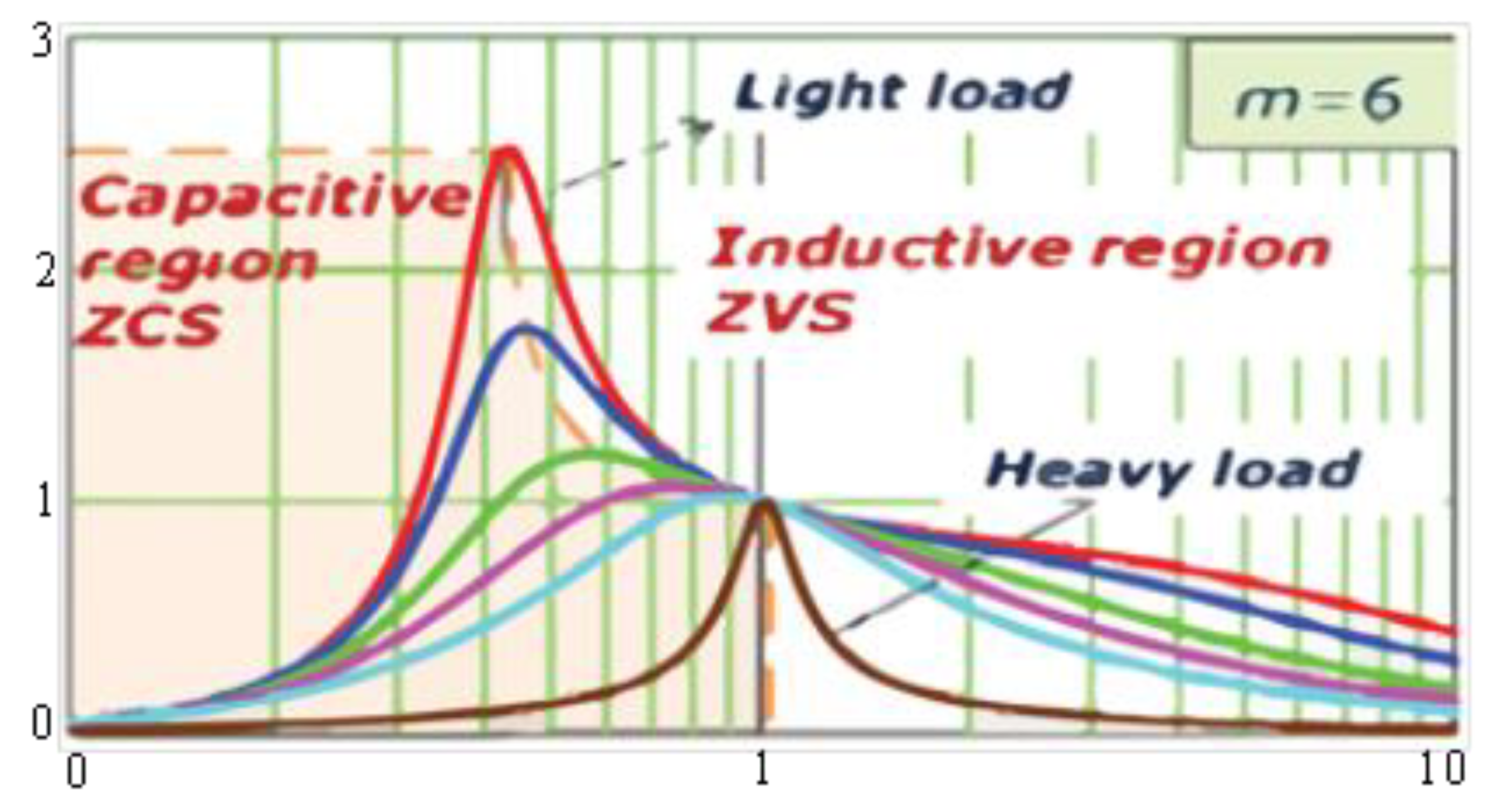
Table 2. The LLC resonant converter’s typical voltage gain curve is shown in
Figure 5. The proposed converter is operated in the inductive region because the LLC resonant converter tank circuit impedance is inductive, and switches are operated with zero voltage switching (ZVS).
BCM boost converter: The boost inductor value can be designed by assuming the converter’s efficiency is greater than 90%, and the maximum bus voltage is up to 410 volts.
Transformer’s turns ratio: The transformer turn ratio can be calculated by assuming a maximum DC bus voltage equal to 410.
Gain calculations: For maximum gain calculation, DC bus voltages should not be less than the peak value of input voltages. So, the maximum and minimum gain can be calculated as:
Selection of A and Q values: The A and Q values are selected by plotting the gain curve for A = 8 and different Q values, shown in
Figure 6.
Gain at Q = 0.35 is slightly higher than the necessary amount. In contrast, the maximum gain at Q = 0.45 is substantially lower than the necessary maximum gain, so, the curve at Q = 0.35 can be chosen for design purposes. Finally, the design is chosen with A = 8 and Q = 0.35. The high frequency, measured in kHz, at which the planned LLC resonant partial power converter operates. It runs at a frequency of 95 kHz.
Resonant frequency: The resonant frequency is determined using the following equation as the ratio of switching frequency (f
s) and normalized frequency (f
n):
The value of ‘
can be calculated from the formula given below:
Resonant inductor: The value of the resonant inductor (
is calculated through the following equation.
Resonant capacitor: The value of the resonant capacitor is (
) calculated through the following equation.
Magnetic inductor: The value of magnetizing inductor (
) is calculated through the following equation.
Coupled inductor: A coupled inductor operates under high frequency, so, a ferrite material core is required instead of a simple iron core. A ferrite core FU2014 with an effective area of 91.8 m
is used which has a maximum flux density of 170 Mt. Equation (23) calculates the number of turns of the coupled inductor.
6. Simulation Results
The proposed system is powered by a 240 V AC, 50 HZ frequency, with output voltages of 60 V and a 100 W output power. To validate the performance and operation, the LED driver is simulated under various test conditions. The results obtained from the simulation are presented in this section.
6.1. No Mismatch in Secondary Windings of Transformer (Case-01)
When both secondary windings have equal magnetic coupling with the transformer’s primary winding.
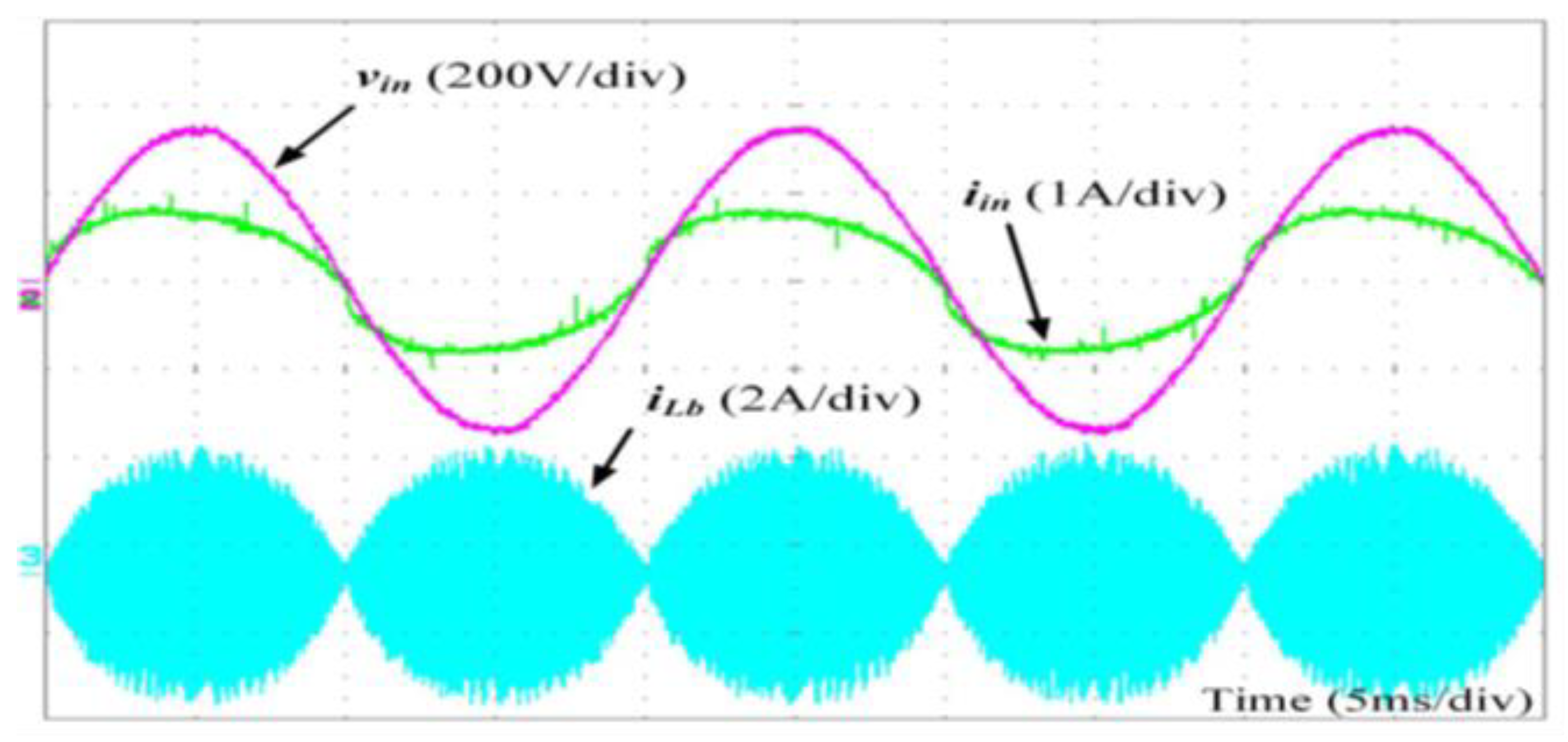
Figure 7 shows that the input voltage and current are in-phase and almost sinusoidal in shape, which means a maximum power factor of 0.99 is achieved with a minimum THD of 10.98 which is very low compared to the existing LED driver. The inductor current (
) work between negative and positive boundaries means that the operation of boost converters in boundary conduction mode provides us with natural power factor correction. The boost inductor current attains maximum peak value as the input power is at its highest.
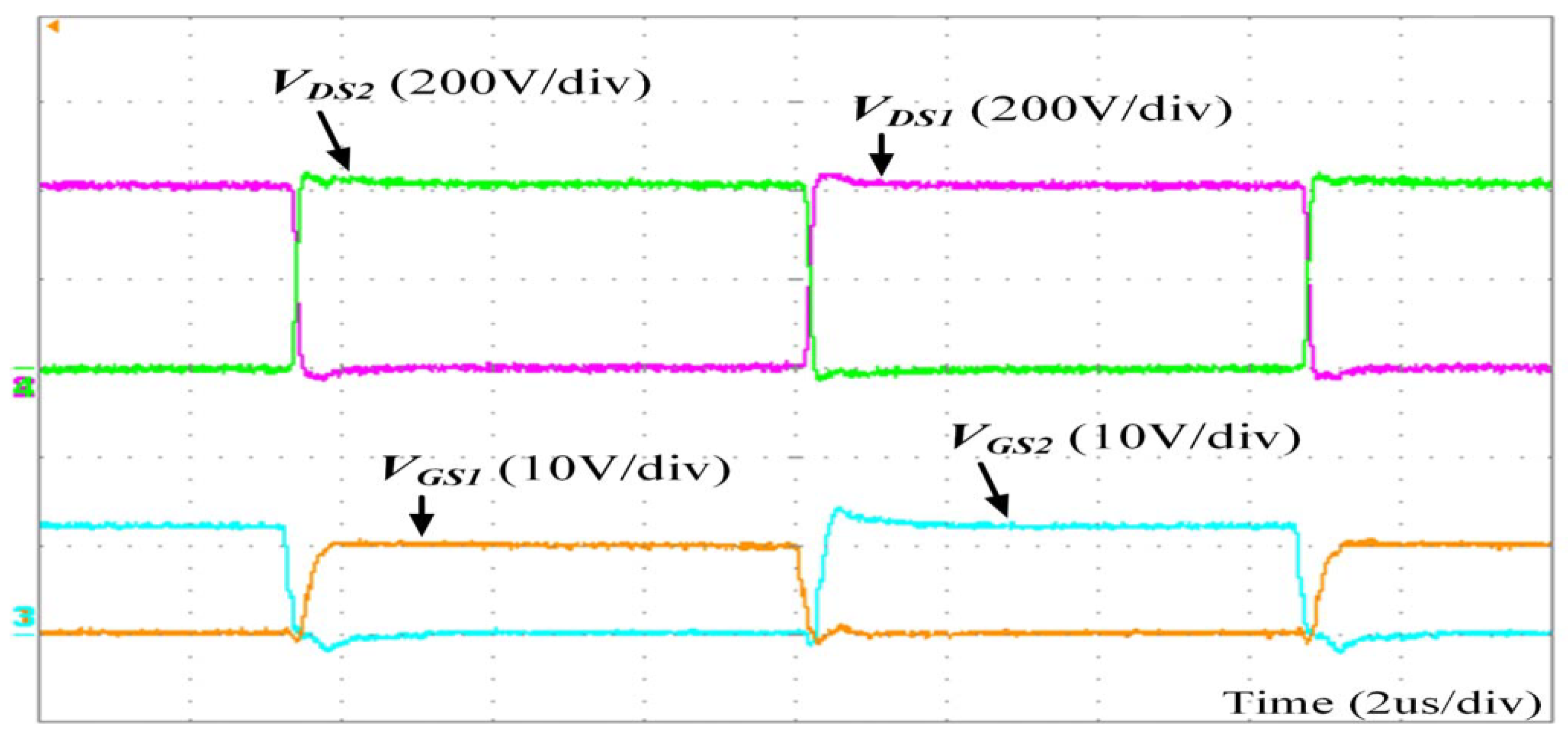
Figure 8 shows the waveforms of switches gate voltage
and
and switches drain source voltage
and
. Increase and decrease in switches source-drain voltage alternately, therefore, two half-bridge switches share voltage stress equally across the bus capacitor. For ZVS operation, a specific dead time was introduced between the consecutive shift of switches.
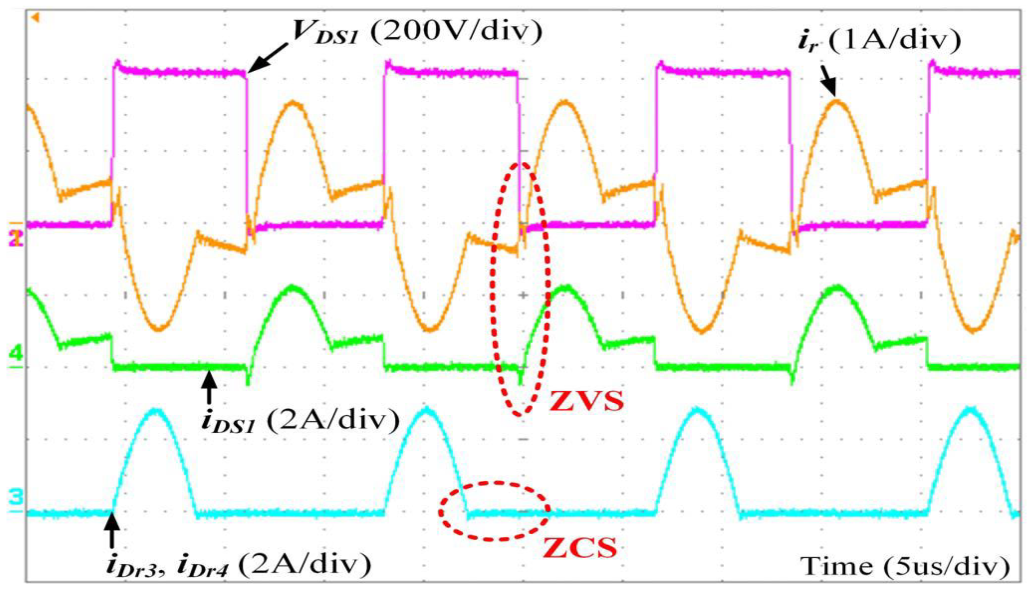
Figure 9 presents simulation waveforms of
VDS1, switch drain-source current
, diodes output current
and
, and resonant current
. Simulation results describe that secondary side diodes are in ZVS mode. The secondary current increases with a sinusoidal shape and becomes zero for a short time interval in each high-frequency switching half cycle with a switching frequency of 78 K Hz and the lowest voltage stresses of about 360 V.
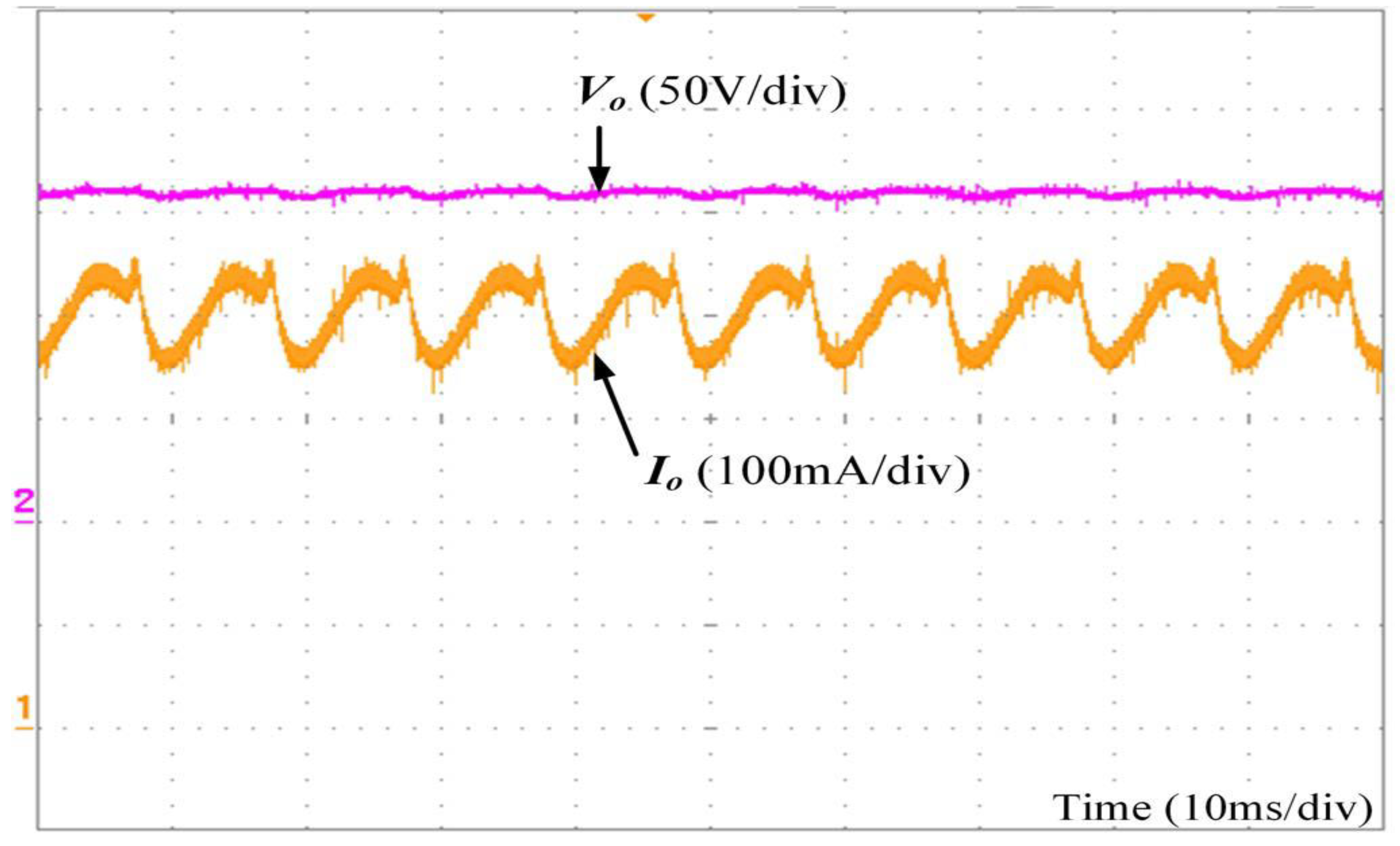
Simulation results of the output current and voltage of both sides are presented in
Figure 10, the voltage is about 60 V, and the current is about 0.82 A on both sides. The large current ripple is double the input AC frequency. The current ripple is approximately 90 mA, while the voltage ripple is less than 5 V. The LEDs illuminated without flickering.
6.2. Mismatch between Secondary Windings (Case-02)
As mentioned above, it is very difficult to make two identical secondary windings because both secondaries cannot achieve the same coupling with the primary winding of the transformer. In this case, the proposed system is analyzed with a 10% mismatch between the windings. The waveform of boost inductor current (
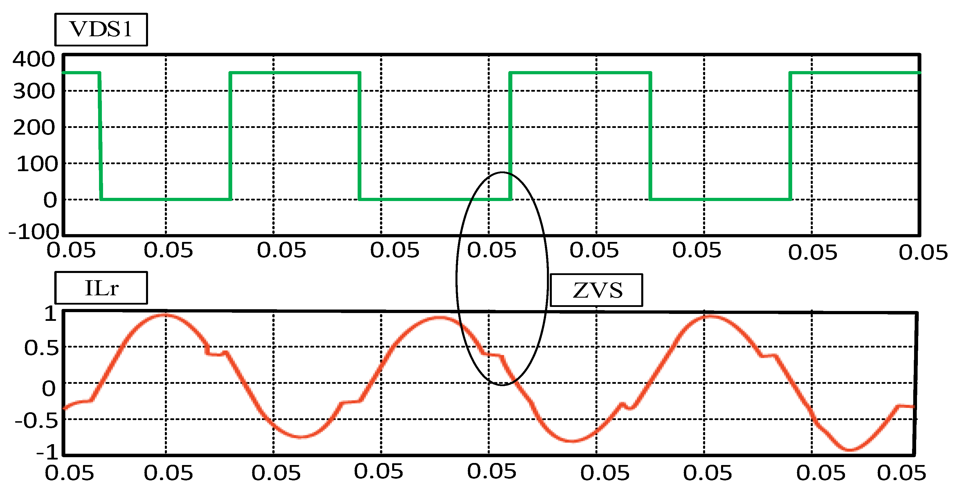
iLb), input voltage, and the input current is the same as in case-1 because boost converters in our proposed system continue to work in boundary conduction mode and improve the power factor. The secondary side diodes attain ZCS, and the switches of the primary side attain ZVS. ZVS of MOSFETs is shown in
Figure 11.
Figure 11 shows the Simulation waveform of magnetizing current and resonant current. These waveforms clearly depict that at a certain time magnetizing current of the transformer and resonant current become equal which means the converter still manages to achieve ZCS.
6.3. Results of Proposed Topology with Coupled Inductor (Case-03)
The effect of coupled inductor simulation is carried out with a 10% mismatch between the secondary windings. Coupled inductor did not affect the power factor correction function; boost converters still operate in boundary conduction mode, which is verified by simulation results. Due to this, the waveform of boost inductor current (
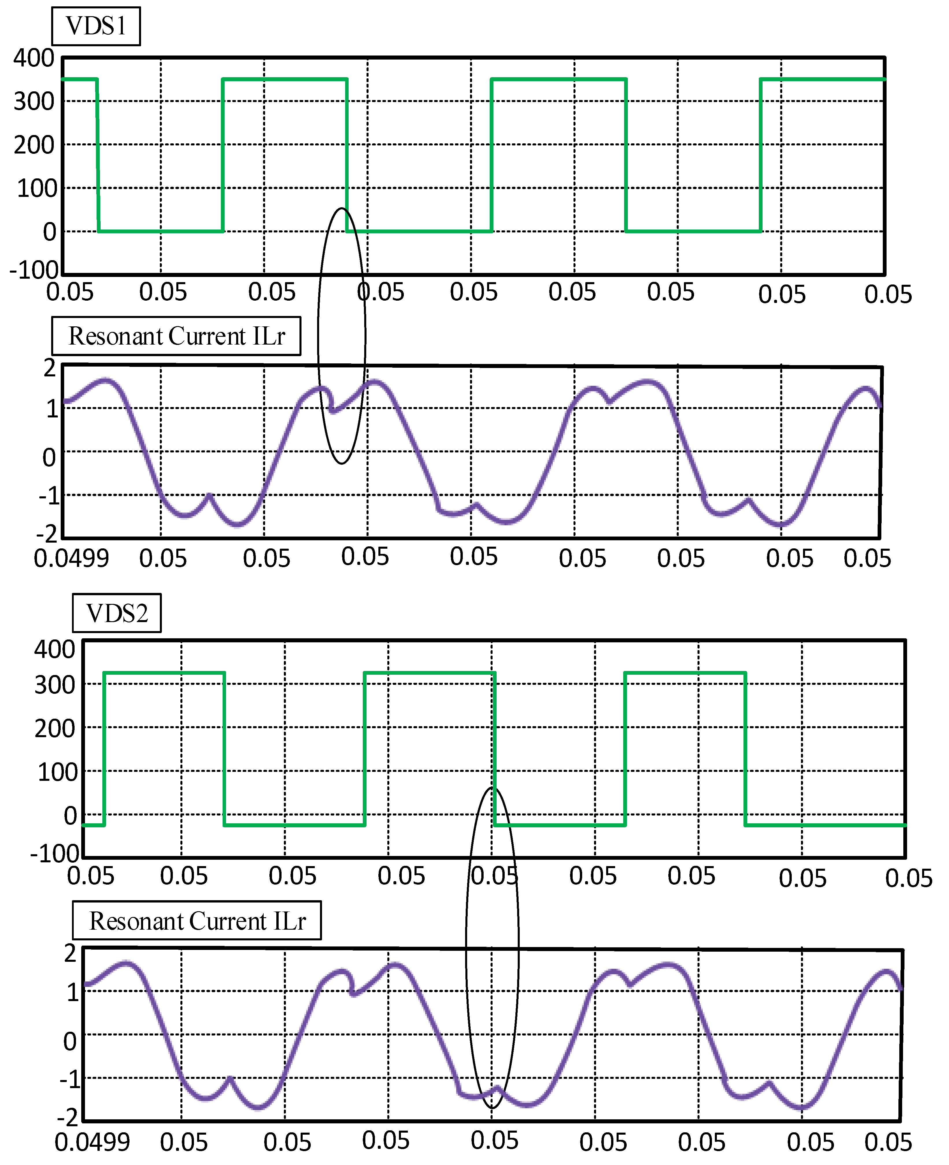
iLb), input voltage, and input current are the same as in case-1. Both switches are operated alternatively, and the stress on the switches is less than 400 V. The LLC resonant converter’s soft-switching features are not disturbed. Both switches are operated in ZVS, as shown in
Figure 12.
In
Figure 12, the waveforms of V
DS1 and ILr and, V
DS2 and ILr show that the soft switching characteristics of the LLC resonant converter are not disturbed. Both switches are operated in ZVS and ZCS. There are some dead intervals in each half cycle of the high-frequency switching cycle which assures the ZCS operation of diodes.
7. Conclusions
A single-stage, 100 W with 240 V AC input, integrated LED driver topology is presented and simulated in this paper; the driver is based on the integration of two boundaries conducted boost converters and a half-bridge LLC resonant converter, and the system has two independent secondary windings which contain the two independent LED strings, both boost converters have a common inductor and operated in boundary conduction mode to realize the power factor correction. Moreover, switching losses are significantly reduced due to the soft switching characteristic of the half-bridge LLC resonant converter, which is verified through simulation results. Two capacitors are used on the input side for voltage division, which reduces the voltage stresses on the switches. The effect of mismatch between two identical windings is also presented in the results, which shows that the voltages of the secondary sides are different from each other. Due to this, the LEDs connected to low-voltage secondary windings do not glow properly. A coupled inductor is added on the secondary side, which encountered the mismatch produced due to unequal magnetic coupling of windings results with mismatch and coupled inductor verified and presented. The addition of coupled inductor does not disturb the performance of the converter and soft switching characteristic (ZVS & ZCS) of the LLC resonant converter, which is verified through simulation results. The size of the DC bus capacitor is also reduced, so that, a film capacitor can be used in practical applications.
In future work, the hardware of the proposed system will be implemented to compare the simulation results with practical results. To improve the circuit’s dependability and luminous efficiency, more LED channels will be added. Additionally, its control circuitry will be changed.
Author Contributions
Conceptualization, J.B., M.L. and M.F.; methodology, L.W., V.S. and M.Z.Y.; software, J.B., M.F., M.L., L.W. and V.S.; validation, J.B., M.L. and M.F.; mathematical analysis, J.B., M.F. and M.Z.Y.; investigation, V.S. and M.F.; resources, L.W., M.L. and M.F.; writing original draft preparation, J.B., M.F. and M.L.; writing review and editing, J.B., V.S., M.F., M.Z.Y. and M.L.; visualization, J.B.; supervision, J.B.; project administration, J.B., M.F. and M.L.; funding acquisition, J.B. All authors have read and agreed to the published version of the manuscript.
Funding
This work is supported by National Natural Science foundation of China (No. U2241221) and national Key Research and Development Program of China (No. 2022YFE0124200). The APA was founded by Mengxin Liu (co-corresponding auther).
Institutional Review Board Statement
Not applicable.
Informed Consent Statement
Not applicable.
Data Availability Statement
Not applicable.
Acknowledgments
The authors are grateful to the School of Microelectronics, Chinese Academy of Sciences, Beijing-China, Institute of Microelectronics of Tianjin, Binhai New Area, China, and School of Electrical and Information Engineering, Hubei University of Automotive Technology Shiyan, China for conducting this research.
Conflicts of Interest
The authors declare no conflict of interest.
References
- Katznelson, R.D.; Howells, J. Inventing-Around Edison’s Incandescent Lamp Patent: Evidence of Patents’ Role in Stimulating Downstream Development; Northwestern University Pritzker School of Law: Chicago, IL, USA, 2012. [Google Scholar]
- Saravanan, M.; Ganesh, N. A single-stage soft-switching LED driver based on CLCL resonant converter and BCM circuit for lighting application. Electr. Eng. 2020, 102, 909–920. [Google Scholar] [CrossRef]
- Bloom, S. Bright light of the future: LEDs take new focus. J. Prop. Manag. 2012, 77, 28–34. [Google Scholar]
- Cheng, C.-A.; Chang, C.-H.; Cheng, H.-L.; Chang, E.-C.; Chung, T.-Y.; Chang, M.-T. A single-stage LED streetlight driver with soft-switching and interleaved PFC features. Electronics 2019, 8, 911. [Google Scholar] [CrossRef]
- Castellanos, J.C.; Turhan, M.; Hendrix, M.A.; van Roermund, A.; Cantatore, E. Dimmable integrated CMOS LED driver based on a resonant DC/DC hybrid-switched capacitor converter. Int. J. Circuit Theory Appl. 2018, 46, 1485–1502. [Google Scholar] [CrossRef]
- Zawawi, N.A.; Iqbal, S.; Jamil, M.K.M. A single-stage power factor corrected LED driver with dual half-wave rectifier. In Proceedings of the 2016 IEEE Industrial Electronics and Applications Conference (IEACon), Kota Kinabalu, Malaysia, 20–22 November 2016. [Google Scholar]
- Li, S.; Tan, S.-C.; Lee, C.K.; Waffenschmidt, E.; Hui, S.; Chi, K.T. A survey, classification, and critical review of light-emitting diode drivers. IEEE Trans. Power Electron. 2015, 31, 1503–1516. [Google Scholar] [CrossRef]
- Lin, W.; Chen, H.; Ke, S. Research on a single-stage Flyback/boost LED driver with lower output ripple. In Proceedings of the 2016 IEEE 2nd Annual Southern Power Electronics Conference (SPEC), Auckland, New Zealand, 5–8 December 2016. [Google Scholar]
- Guo, Y. Single-Stage AC/DC Single-Inductor Multiple-Output (SIMO) LED Drivers; HKU Theses Online (HKUTO); The University of Hong Kong: Hong Kong, China, 2016. [Google Scholar]
- Athalye, P.; Harris, M.; Negley, G. A two-stage LED driver for high-performance high-voltage LED fixtures. In Proceedings of the 2012 Twenty-Seventh Annual IEEE Applied Power Electronics Conference and Exposition (APEC), Orlando, FL, USA, 5–9 February 2012. [Google Scholar]
- Wang, Y.; Guan, Y.; Xu, D.; Wang, W. A CLCL resonant DC/DC converter for two-stage LED driver system. IEEE Trans. Ind. Electron. 2015, 63, 2883–2891. [Google Scholar] [CrossRef]
- Xie, X.; Ye, M.; Cai, Y.; Wu, J. An optocouplerless two-stage high power factor LED driver. In Proceedings of the 2011 Twenty-Sixth Annual IEEE Applied Power Electronics Conference and Exposition (APEC), Fort Worth, TX, USA, 6–11 March 2011. [Google Scholar]
- Lin, W.; Xu, Y.; Zheng, Q.L. A high efficiency integrated step-down Cuk and flyback converter for LED power driver. In Proceedings of the 2015 9th International Conference on Power Electronics and ECCE Asia (ICPE-ECCE Asia), Seoul, Republic of Korea, 1–5 June 2015. [Google Scholar]
- Wang, Y.; Deng, X.; Wang, Y.; Xu, D. Single-stage bridgeless LED driver based on a CLCL resonant converter. IEEE Trans. Ind. Appl. 2017, 54, 1832–1841. [Google Scholar] [CrossRef]
- Samuel, B.S.; Naik, R.S. A Universal-Input Single-Stage High-Power-Factor Power Supply for LEDs Based on Integrated Double Buck-Boost Converter. Int. J. Sci. Eng. Technol. Res. 2015, 4, 1009–1013. [Google Scholar]
- Chen, S.-Y.; Li, Z.R.; Chen, C.-L. Analysis and design of single-stage AC/DC LLC resonant converter. IEEE Trans. Ind. Electron. 2011, 59, 1538–1544. [Google Scholar] [CrossRef]
- Muneer, A.; Fayyaz, A.; Iqbal, S.; Jabbar, M.W.; Qaisar, A.; Farooq, F. Single Stage Active Power Factor Correction Circuit for Street LED Light with Battery Backup. Eng. Proc. 2022, 12, 69. [Google Scholar] [CrossRef]
- Ma, J.; Wei, X.; Hu, L.; Zhang, J. LED driver based on boost circuit and LLC converter. IEEE Access 2018, 6, 49588–49600. [Google Scholar] [CrossRef]
- Cheng, C.-A.; Chang, C.-H.; Chung, T.-Y.; Yang, F.-L. Design and implementation of a single-stage driver for supplying an LED street-lighting module with power factor corrections. IEEE Trans. Power Electron. 2014, 30, 956–966. [Google Scholar] [CrossRef]
- Camponogara, D.; Vargas, D.R.; Dalla Costa, M.A.; Alonso, J.M.; Garcia, J.; Marchesan, T. Capacitance reduction with an optimized converter connection applied to LED drivers. IEEE Trans. Ind. Electron. 2014, 62, 184–192. [Google Scholar] [CrossRef]
- Serna Tamez, A. Non-Energy Benefits Brought by the Use of Variable Frequency Drives in Pump and Fan Applications. Master’s Thesis, Utrecht University, Utrecht, The Netherlands, 2019. [Google Scholar]
- Zawawi, N.A.; Iqbal, S.; Jamil, M.K.M. Implementation of a single-stage LED driver using resonant controller. In Proceedings of the 2016 6th International Conference on Intelligent and Advanced Systems (ICIAS), Kuala Lumpur, Malaysia, 15–17 August 2016. [Google Scholar]
- Fang, P.; Webb, S.; Liu, Y.F.; Sen, P.C. Single-stage LED driver achieves electrolytic capacitor-less and flicker-free operation with unidirectional current compensator. IEEE Trans. Power Electron. 2018, 34, 6760–6776. [Google Scholar] [CrossRef]
- Yan, Y.-H.; Cheng, H.L.; Cheng, C.A.; Chang, Y.N.; Wu, Z.X. A Novel Single-Switch Single-Stage LED Driver with Power Factor Correction and Current Balancing Capability. Electronics 2021, 10, 1340. [Google Scholar] [CrossRef]
| Disclaimer/Publisher’s Note: The statements, opinions and data contained in all publications are solely those of the individual author(s) and contributor(s) and not of MDPI and/or the editor(s). MDPI and/or the editor(s) disclaim responsibility for any injury to people or property resulting from any ideas, methods, instructions or products referred to in the content. |
© 2023 by the authors. Licensee MDPI, Basel, Switzerland. This article is an open access article distributed under the terms and conditions of the Creative Commons Attribution (CC BY) license (https://creativecommons.org/licenses/by/4.0/).
