
Analysis and Design of Series-LC-Switch Capacitor Multistage High Gain DC-DC Boost Converter for Electric Vehicle Applications

 ,
,  ,
, 
 and
and 
Abstract
:1. Introduction
Contribution
- The overall number of inductors, capacitors, and switches have been largely reduced. Now, only one inductor, capacitor, and switch are required for use in the single-stage boost converter. This reduces the overall size and cost of the system.
- The multiple-stage boost converters are easily extendable and gain can be easily adjusted according to requirements. The PWM signal is used to control only one switch, which controls the single-stage overall gain.
- The proposed design aims to reduce both device voltage and current stress in order to reduce device size. In this way, device power capacity is utilized to its maximum.
- The proposed DC-DC converter serves as a good option for use in both EV driving and battery charging systems.
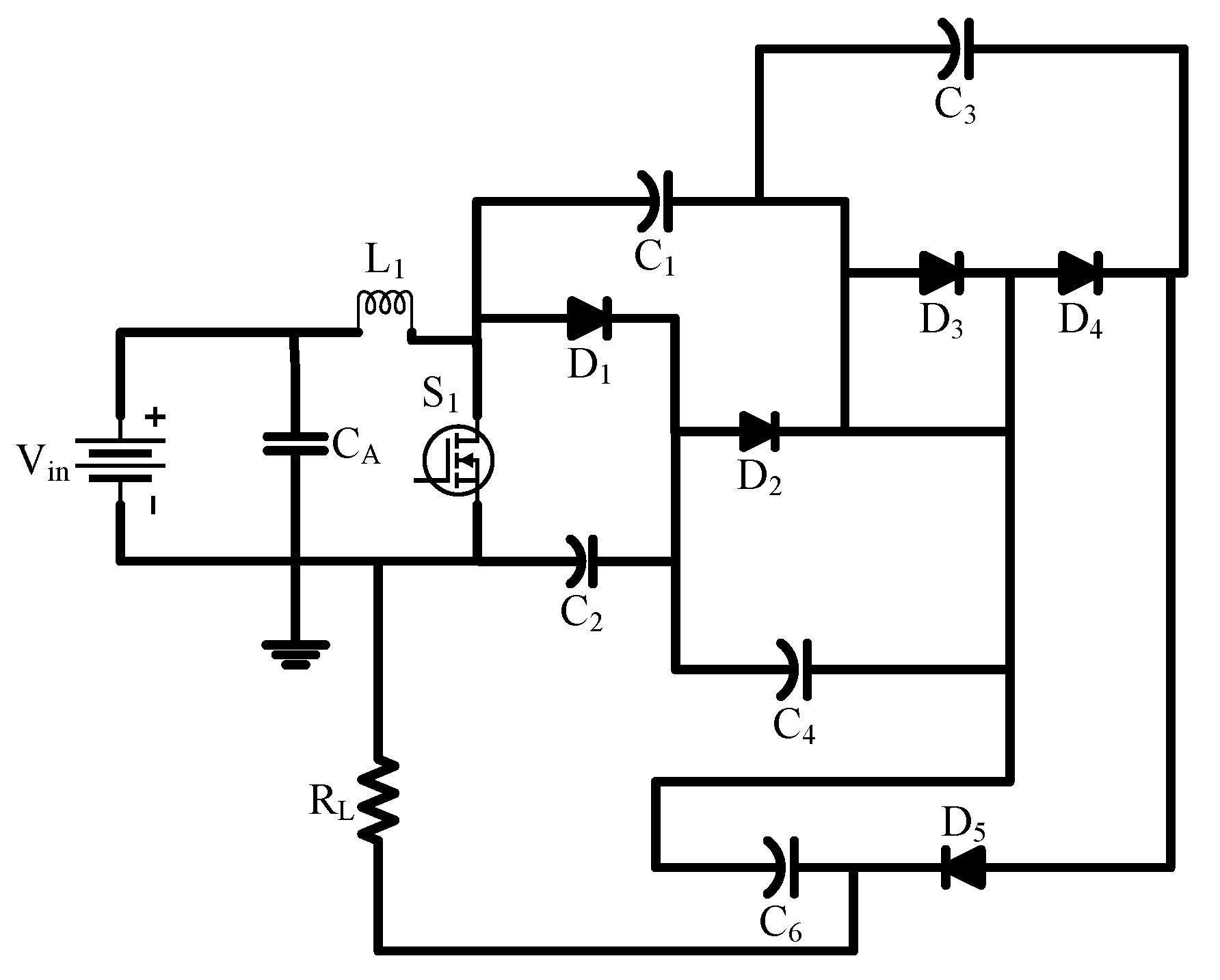
2. Modelling and Operation of the Proposed Converter
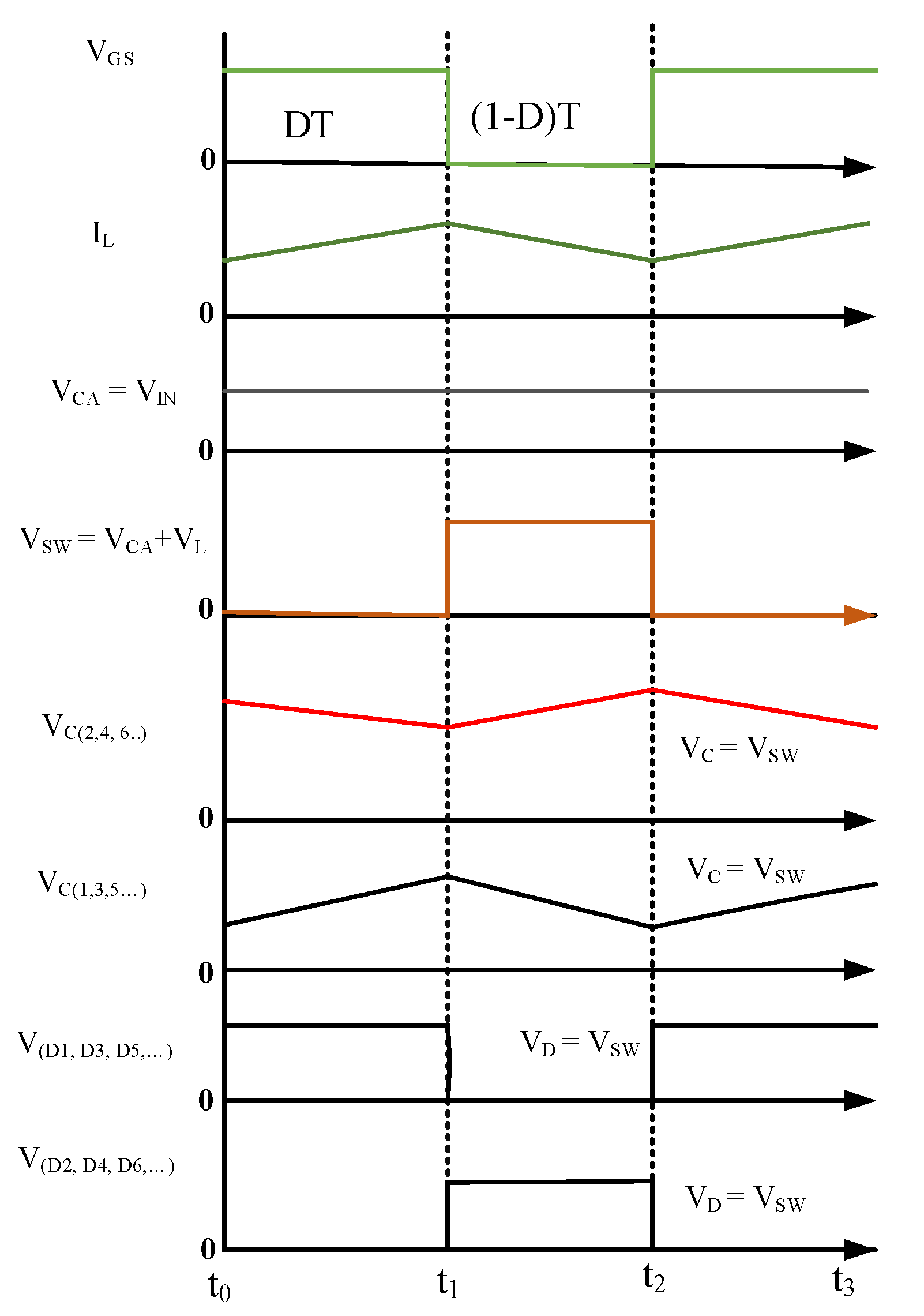
2.1. CCM Operation
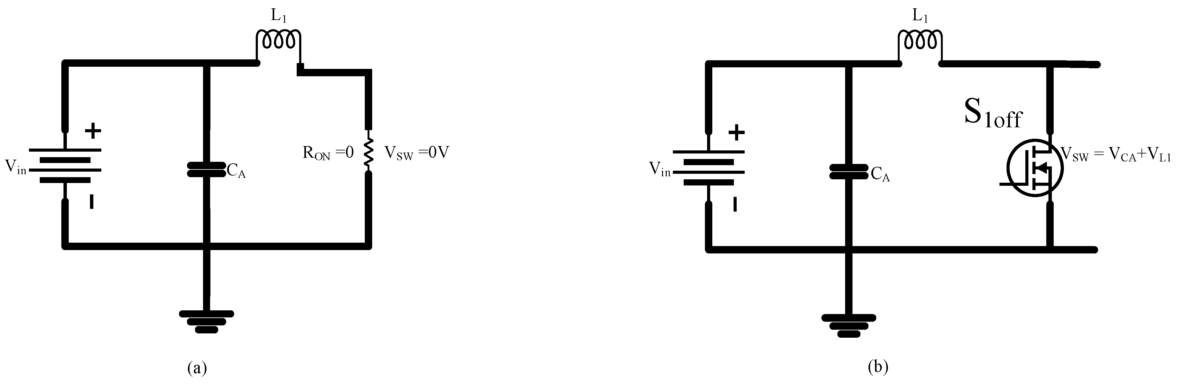
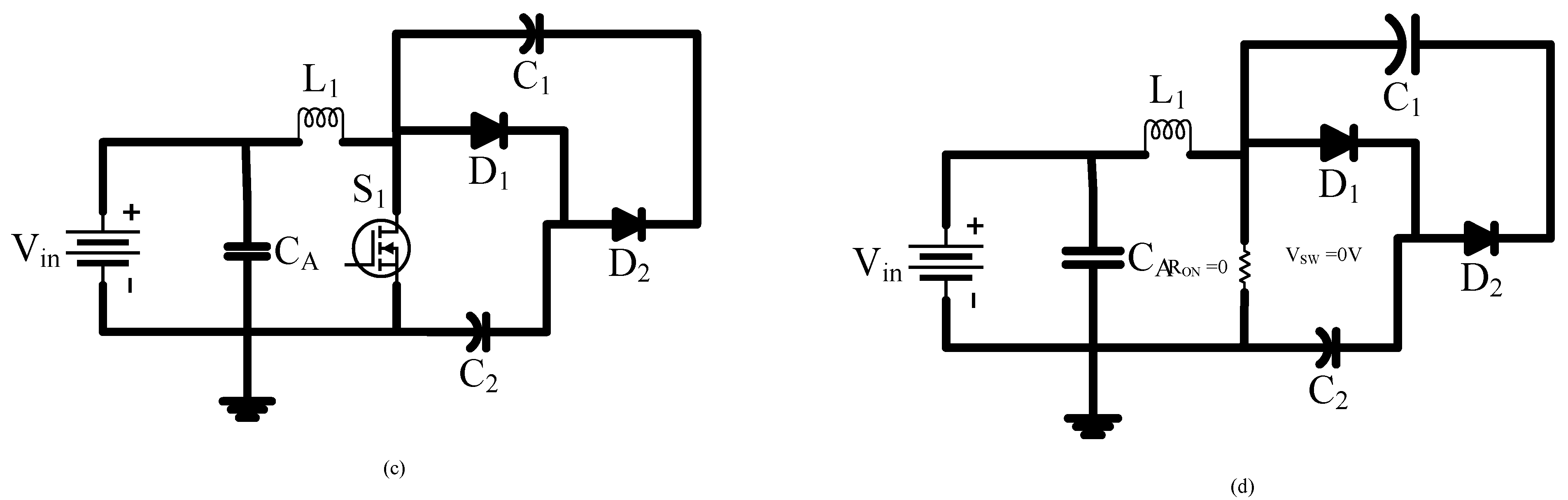
2.2. Mode 1
2.3. Mode 2
2.4. Mode 1
2.5. Converter Gain
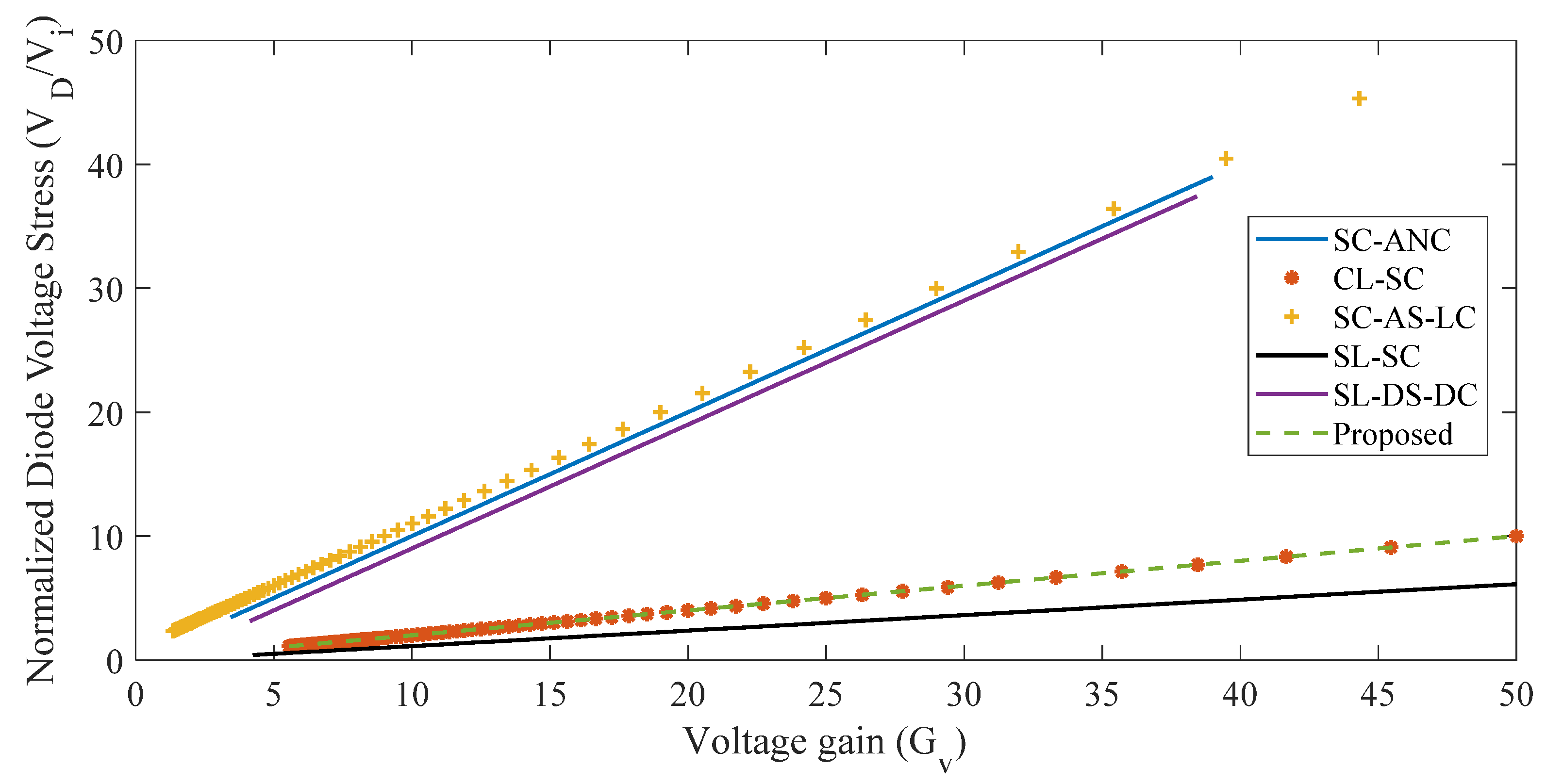
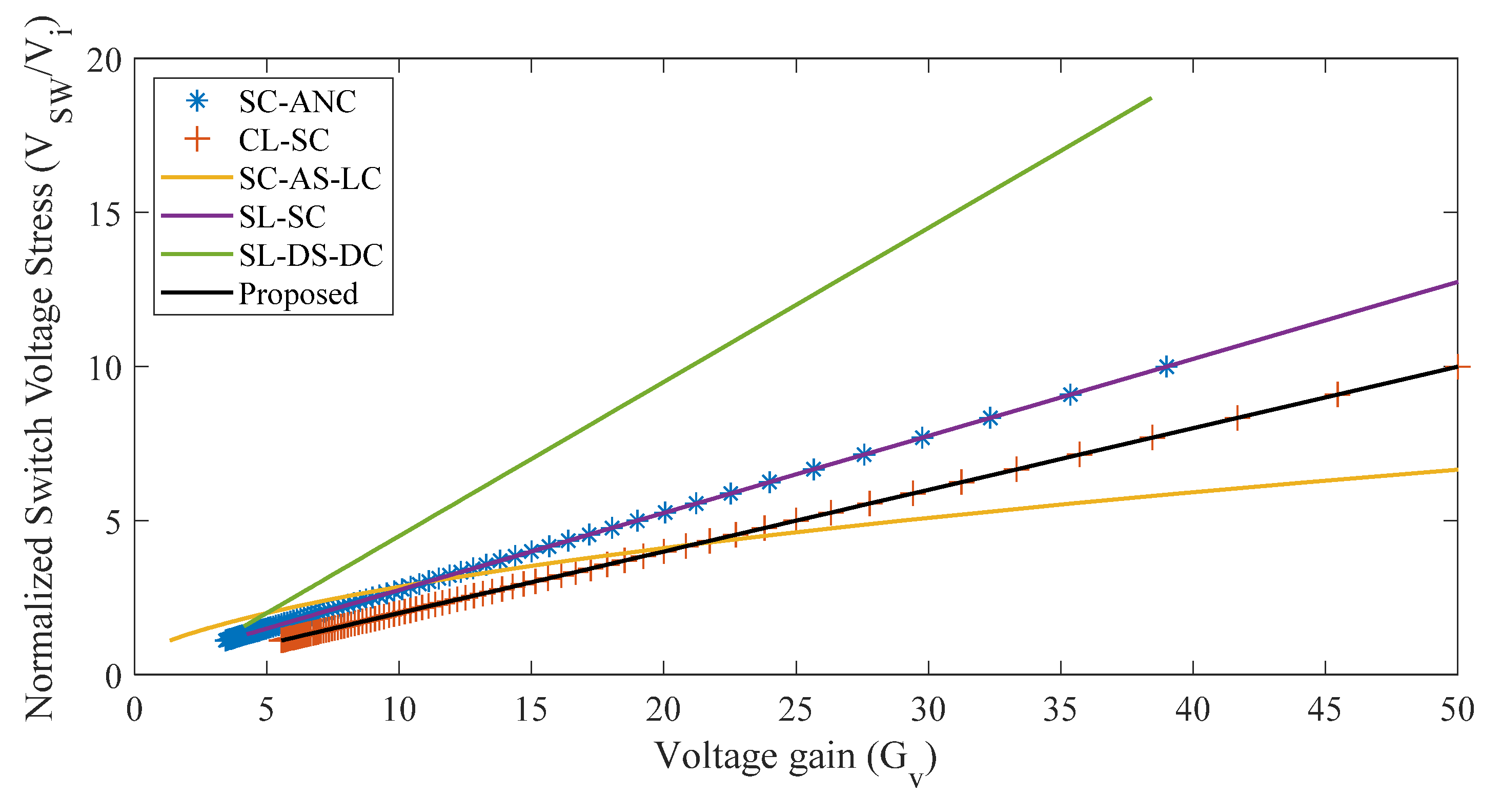
2.6. Voltage Stress
2.7. Current Stress
3. Analysis of the Proposed Converter
3.1. Voltage and Current Gain Analysis
3.2. Steady-State Analysis
3.3. Loss Analysis
3.4. Design Analysis
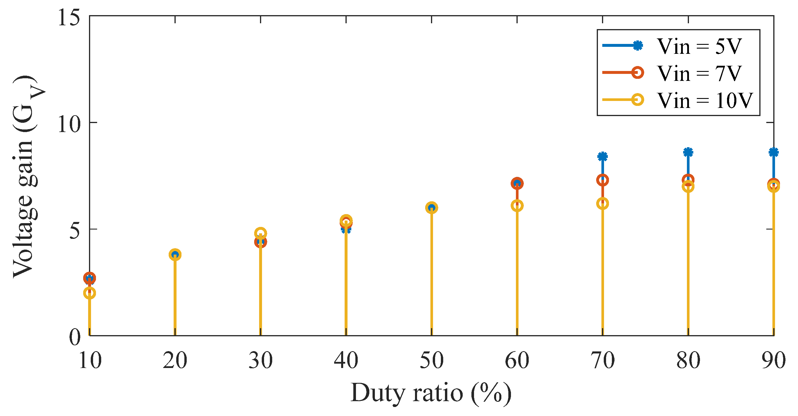
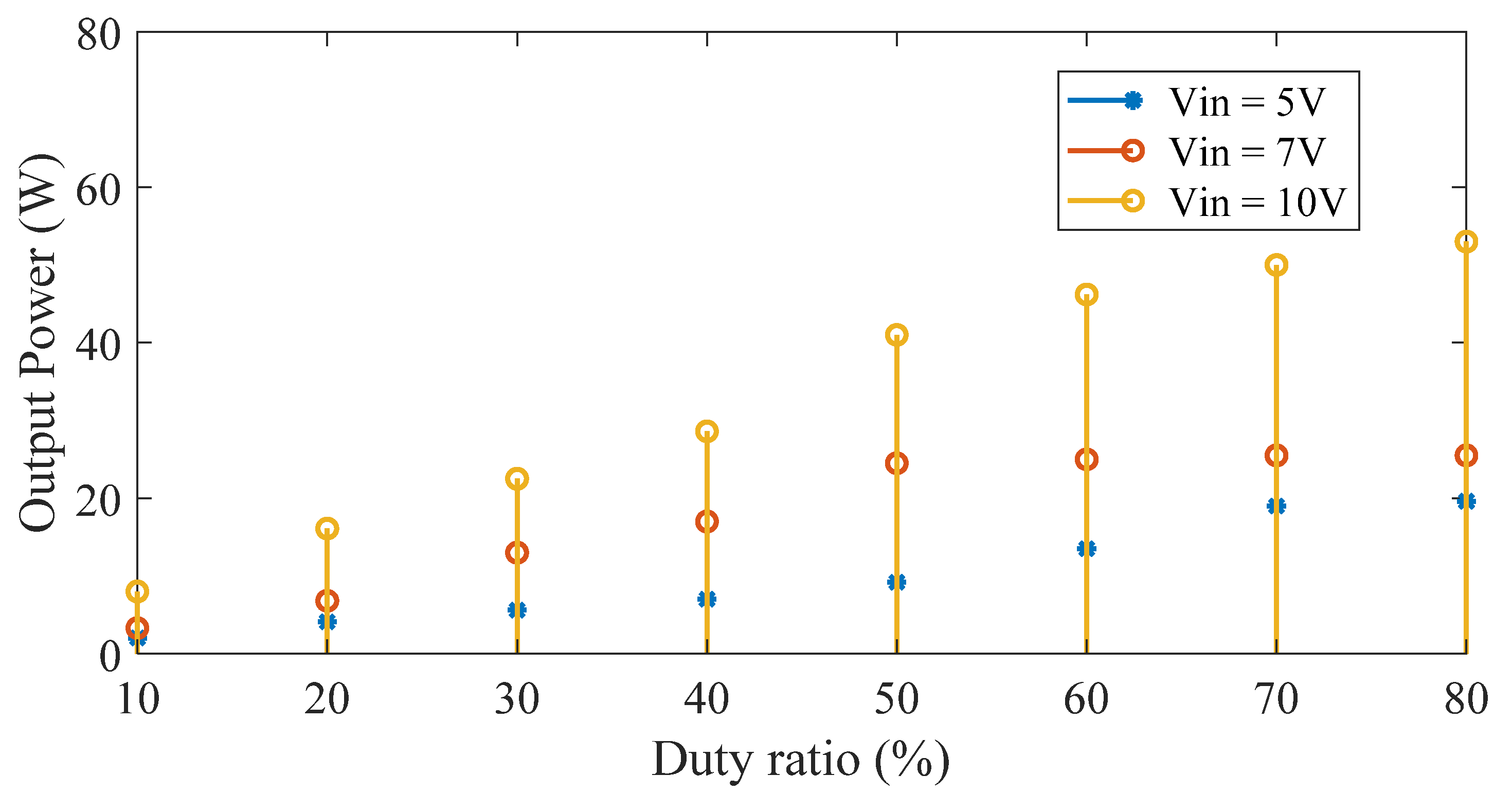
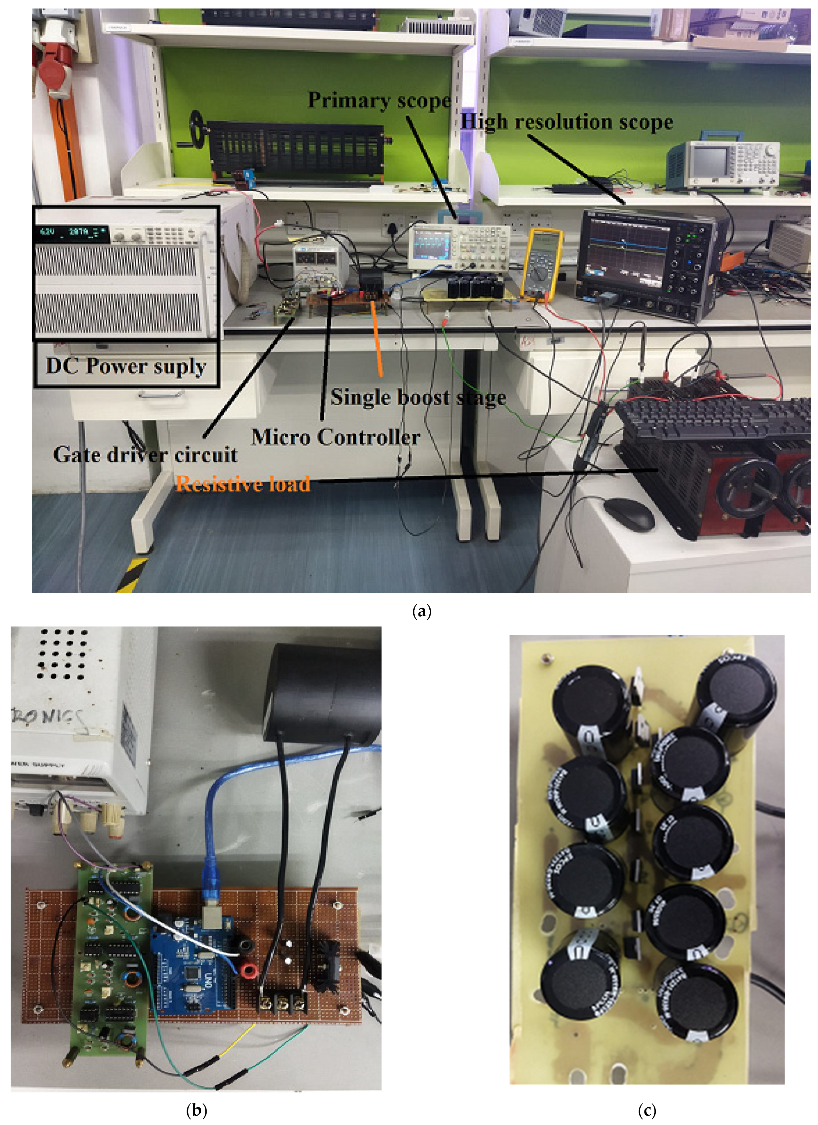
4. Experimental Results and Discussion
5. Conclusions
6. Future Challenges
Author Contributions
Funding
Institutional Review Board Statement
Informed Consent Statement
Data Availability Statement
Acknowledgments
Conflicts of Interest
Nomenclature
| Symbol | Meaning |
| ∆i | incremental current |
| ∆Q | incremental charge |
| ∆V | incremental voltage |
| CCM | continues conduction mode |
| CL-SC | coupled inductor switch capacitor |
| Cn | nth capacitor |
| Cosc | output cside capacitance |
| D | duty cycle ratio |
| ESR | equivalent series resistor |
| EV | electric vehicle |
| fsw | switching frequency |
| Gv | voltage gain |
| I0 | output current |
| ICE | inter combustible engine |
| Iin | input current |
| IMF | International Monetary Fund |
| Ln | nth inductor |
| NVS | normalized voltage stress |
| Pc | conduction power loss |
| PD | diode power loass |
| PL | inductor power loss |
| Ploss | total power loss |
| Po | output power |
| Psw | switch power loss |
| QZS | Z-source & quasi Z source |
| RL | load resistance |
| SC | switch capacitor |
| SC-ANC | switch capacitor active netowrk converter |
| SL | switch inductor |
| SL-DS-DC | switch inductor double switch DC convertor |
| Sn | nth switch |
| VL | voltage across inductor |
| VMC | voltage multiplier circuit |
| VSI | voltage source inverter |
| Vsw | Switch voltage |
| ZCS | zero current switching |
| ZVS | zero voltage switching |
References
- Reda, C.; Fuad Hasanov, A.P. Riding the Energy Transition: Oil Beyond 2040. IMF Working Papers, Working Paper No. 17/120. 2017. Available online: https://www.imf.org/en/Publications/WP/Issues/2017/05/22/Riding-the-Energy-Transition-Oil-Beyond-2040-44932 (accessed on 1 January 2022).
- Das, H.S.; Rahman, M.M.; Li, S.; Tan, C.W. Electric vehicles standards, charging infrastructure, and impact on grid integration: A technological review. Renew. Sustain. Energy Rev. 2020, 120, 109618. [Google Scholar] [CrossRef]
- Song, Y.; Wang, B. Evaluation Methodology and Control Strategies for Improving Reliability of HEV Power Electronic System. IEEE Trans. Veh. Technol. 2014, 63, 3661–3676. [Google Scholar] [CrossRef]
- Hsu, Y.-C.; Kao, S.-C.; Ho, C.-Y.; Jhou, P.-H.; Lu, M.-Z.; Liaw, C.-M. On an Electric Scooter With G2V/V2H/V2G and Energy Harvesting Functions. IEEE Trans. Power Electron. 2018, 33, 6910–6925. [Google Scholar] [CrossRef]
- INL Advanced Vehicles—Vehicle Testing. Available online: https://avt.inl.gov/vehicle-type/all-powertrain-architecture (accessed on 1 January 2022).
- Chen, H.; Kim, H.; Erickson, R.; Maksimovic, D. Electrified Automotive Powertrain Architecture Using Composite DC–DC Converters. IEEE Trans. Power Electron. 2017, 32, 98–116. [Google Scholar] [CrossRef]
- Janabi, A.; Wang, B. Switched-Capacitor Voltage Boost Converter for Electric and Hybrid Electric Vehicle Drives. IEEE Trans. Power Electron. 2020, 35, 5615–5624. [Google Scholar] [CrossRef]
- Niu, S.; Xu, H.; Sun, Z.; Shao, Z.Y.; Jian, L. The state-of-the-arts of wireless electric vehicle charging via magnetic resonance: Principles, standards and core technologies. Renew. Sustain. Energy Rev. 2019, 114, 109302. [Google Scholar] [CrossRef]
- Song, S.; Zhang, Q.; He, Z.; Li, H.; Zhang, X. Uniform Power Dynamic Wireless Charging System With I-Type Power Supply Rail and DQ-Phase-Receiver Employing Receiver-Side Control. IEEE Trans. Power Electron. 2020, 35, 11205–11212. [Google Scholar] [CrossRef]
- Zhao, Q.; Wang, A.; Liu, J.; Wang, X. The Load Estimation and Power Tracking Integrated Control Strategy for Dual-Sides Controlled LCC Compensated Wireless Charging System. IEEE Access 2019, 7, 75749–75761. [Google Scholar] [CrossRef]
- Mohamed, A.A.S.; An, S.; Mohammed, O. Coil Design Optimization of Power Pad in IPT System for Electric Vehicle Applications. IEEE Trans. Magn. 2018, 54, 1–5. [Google Scholar] [CrossRef]
- Bai, C.; Han, B.; Kwon, B.-H.; Kim, M. Highly Efficient Bidirectional Series-Resonant DC/DC Converter Over Wide Range of Battery Voltages. IEEE Trans. Power Electron. 2020, 35, 3636–3650. [Google Scholar] [CrossRef]
- Rajaei, A.; Khazan, R.; Mahmoudian, M.; Mardaneh, M.; Gitizadeh, M. A Dual Inductor High Step-Up DC/DC Converter Based on the Cockcroft–Walton Multiplier. IEEE Trans. Power Electron. 2018, 33, 9699–9709. [Google Scholar] [CrossRef]
- Faridpak, B.; Bayat, M.; Nasiri, M.; Samanbakhsh, R.; Farrokhifar, M. Improved Hybrid Switched Inductor/Switched Capacitor DC–DC Converters. IEEE Trans. Power Electron. 2021, 36, 3053–3062. [Google Scholar] [CrossRef]
- Liu, H.-C.; Li, F. Novel High Step-Up DC–DC Converter with an Active Coupled-Inductor Network for a Sustainable Energy System. IEEE Trans. Power Electron. 2015, 30, 6476–6482. [Google Scholar] [CrossRef]
- Xu, Y.; Wang, K.; Jin, L.; Deng, Y.; Lu, Y.; Yang, Y. Isolated Multi-port DC-DC Converter-Based on Bifurcate MMC Structure. In Proceedings of the 2019 IEEE PES Asia-Pacific Power and Energy Engineering Conference (APPEEC), Macao, China, 1–4 December 2019; pp. 1–6. [Google Scholar]
- Salvador, M.A.; Lazzarin, T.B.; Coelho, R.F. High Step-Up DC–DC Converter With Active Switched-Inductor and Passive Switched-Capacitor Networks. IEEE Trans. Ind. Electron. 2018, 65, 5644–5654. [Google Scholar] [CrossRef]
- Debnath, D.; Chatterjee, K. Two-Stage Solar Photovoltaic-Based Stand-Alone Scheme Having Battery as Energy Storage Element for Rural Deployment. IEEE Trans. Ind. Electron. 2015, 62, 4148–4157. [Google Scholar] [CrossRef]
- Muhammad, M.; Armstrong, M.; Elgendy, M.A. Analysis and implementation of high-gain non-isolated DC–DC boost converter. IET Power Electron. 2017, 10, 1241–1249. [Google Scholar] [CrossRef] [Green Version]
- Forouzesh, M.; Siwakoti, Y.P.; Gorji, S.A.; Blaabjerg, F.; Lehman, B. Step-Up DC–DC Converters: A Comprehensive Review of Voltage-Boosting Techniques, Topologies, and Applications. IEEE Trans. Power Electron. 2017, 32, 9143–9178. [Google Scholar] [CrossRef]
- Malik, M.Z.; Chen, H.; Nazir, M.S.; Khan, I.A.; Abdalla, A.N.; Ali, A.; Chen, W. A New Efficient Step-Up Boost Converter with CLD Cell for Electric Vehicle and New Energy Systems. Energies 2020, 13, 1791. [Google Scholar] [CrossRef] [Green Version]
- Wu, G.; Ruan, X.; Ye, Z. Nonisolated High Step-Up DC–DC Converters Adopting Switched-Capacitor Cell. IEEE Trans. Ind. Electron. 2015, 62, 383–393. [Google Scholar] [CrossRef]
- Ahmad, J.; Siddique, M.D.; Sarwar, A.; Lin, C.H.; Iqbal, A. A high gain noninverting DC–DC converter with low voltage stress for industrial applications. Int. J. Circuit Theory Appl. 2021, 49, 4212–4230. [Google Scholar] [CrossRef]
- Tang, Y.; Wang, T.; He, Y. A Switched-Capacitor-Based Active-Network Converter With High Voltage Gain. IEEE Trans. Power Electron. 2014, 29, 2959–2968. [Google Scholar] [CrossRef]
- Veerachary, M.; Kumar, P. Analysis and Design of Quasi-Z-Source Equivalent DC–DC Boost Converters. IEEE Trans. Ind. Appl. 2020, 56, 6642–6656. [Google Scholar] [CrossRef]
- Gu, Y.; Chen, Y.; Zhang, B.; Qiu, D.; Xie, F. High Step-Up DC–DC Converter With Active Switched LC-Network for Photovoltaic Systems. IEEE Trans. Energy Convers. 2019, 34, 321–329. [Google Scholar] [CrossRef]
- Bao, D.; Kumar, A.; Pan, X.; Xiong, X.; Beig, A.R.; Singh, S.K. Switched Inductor Double Switch High Gain DC-DC Converter for Renewable Applications. IEEE Access 2021, 9, 14259–14270. [Google Scholar] [CrossRef]


| Components | Device Specifications | Quantity | Parameter |
|---|---|---|---|
| Regulatable DC power supply | 600 V, 20 A | 1 | |
| Resistive Load | Variable | 2 | 150 , 1 A |
| Output DC voltage | 5 ports | ||
| Adjustable output power | |||
| Switching frequency | PWM | - | |
| Inductor | |||
| Capacitors | Electrolytic | 9 | , |
| Power Switch | Infineon IPW60R045P | 1 | 650 V, 60 A, 45 m |
| Diodes | VS-15TQ060-M3 | 8 | VBR = 1000, 15 A |
| Microcontroller | Arduini UNO | 1 | - |
| Oscilloscope | Lecroy waveRunner | 1 | - |
| Loss Types | D = 10% | D = 20% | D = 30% | D = 40% | D = 50% | D = 60% | D = 70% |
|---|---|---|---|---|---|---|---|
| 37 | 110 | 205 | 390 | 950 | 1300 | 2500 | |
| 2 | 1.5 | 1.5 | 1.8 | 2.3 | 2.3 | 2.3 | |
| 240 | 240 | 320 | 360 | 280 | 250 | 260 | |
| 760 | 380 | 400 | 260 | 260 | 260 | 360 | |
| Output power | 7.8 | 16.5 | 21 | 28.6 | 40.9 | 46.2 | 50.4 |
| 88 | 95.7 | 95.77 | 96.5 | 96.4 | 96.2 | 94.2 |
Publisher’s Note: MDPI stays neutral with regard to jurisdictional claims in published maps and institutional affiliations. |
© 2022 by the authors. Licensee MDPI, Basel, Switzerland. This article is an open access article distributed under the terms and conditions of the Creative Commons Attribution (CC BY) license (https://creativecommons.org/licenses/by/4.0/).
Share and Cite
Khalid, H.; Mekhilef, S.; Mubin, M.B.; Seyedmahmoudian, M.; Stojcevski, A.; Rawa, M.; Horan, B. Analysis and Design of Series-LC-Switch Capacitor Multistage High Gain DC-DC Boost Converter for Electric Vehicle Applications. Sustainability 2022, 14, 4495. https://doi.org/10.3390/su14084495
Khalid H, Mekhilef S, Mubin MB, Seyedmahmoudian M, Stojcevski A, Rawa M, Horan B. Analysis and Design of Series-LC-Switch Capacitor Multistage High Gain DC-DC Boost Converter for Electric Vehicle Applications. Sustainability. 2022; 14(8):4495. https://doi.org/10.3390/su14084495
Chicago/Turabian StyleKhalid, Hassan, Saad Mekhilef, Marizan Binti Mubin, Mehdi Seyedmahmoudian, Alex Stojcevski, Muhyaddin Rawa, and Ben Horan. 2022. "Analysis and Design of Series-LC-Switch Capacitor Multistage High Gain DC-DC Boost Converter for Electric Vehicle Applications" Sustainability 14, no. 8: 4495. https://doi.org/10.3390/su14084495
APA StyleKhalid, H., Mekhilef, S., Mubin, M. B., Seyedmahmoudian, M., Stojcevski, A., Rawa, M., & Horan, B. (2022). Analysis and Design of Series-LC-Switch Capacitor Multistage High Gain DC-DC Boost Converter for Electric Vehicle Applications. Sustainability, 14(8), 4495. https://doi.org/10.3390/su14084495