1. Introduction
The present alarming situation of depletion of non-renewable energy sources presents an opportunity to look for alternative energy sources. RESs are a good option to replace fossil fuel energy and nuclear energy for electrical power generation. In recent years, the share of RESs in power generation has increased significantly. Distributed generation (DG) technologies utilize RESs in the form of solar cells, fuel cells and wind turbines etc. [
1,
2]. To tackle the problem of environmental pollution and global warming caused by fossil fuels, sustainable energy production can be achieved by renewable [
3,
4] energy sources. Renewable energy systems and energy storage systems are going to play an important role in the future of low-carbon energy emission systems [
5].
RESs are integrated with battery energy storage systems (BESSs), are not only environmentally friendly but also result in the wide use of DC (Direct Current) systems, i.e., DC generation and DC storage units. To inject this power into the alternating current (AC) Distribution Grid, DC-AC power electronic converters are used. Similarly, AC–DC and DC–AC conversion are used in AC drives. Moreover, the DC loads such as electric vehicles (EVs), light-Emitting Diode systems (LED), DC motors, data centres, and other battery-based devices are penetrating the market with a rising curve [
6]. These systems require AC–DC conversion systems, so there are multiple stages of AC–DC conversion, which reduce the overall efficiency and reliability of the systems. The increasing demand for DC power at load has challenged the conventional AC distribution system, while the DC power systems are used for the transfer of DC power over long distances, mostly in high-voltage applications. The advantages of DC power systems have not been exploited in low voltage (LV) (1.5 kV) and medium voltage (MV) (50 kV), leaving the power system domain to AC architecture [
6,
7]. To solve this problem, the concept of a DC microgrid is derived to meet local demands. Microgrids are interconnected to LV and MV distribution networks via direct connection or a power electronic interface. Easier integration of RESs and BESSs with DC microgrid means that the supply does not need to be converted into AC; instead of the multiple AC–DC and DC–AC converter, DC power could be supplied by a DC-DC converter, resulting in the reduction of primary energy consumption, leading to efficient and smaller systems. Therefore, it is more efficient to have a DC distribution, including DC-DC converters, than AC counterparts [
8].
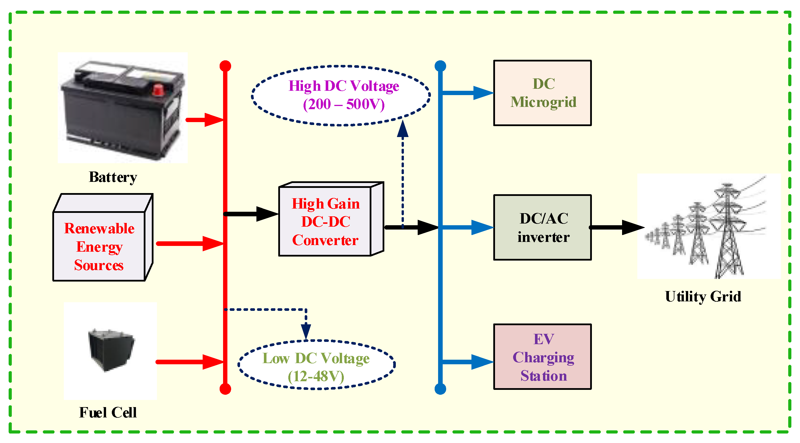
Figure 1 shows the arrangement for RESs, which generate low output voltage (12–48 V), so output voltage has to be lifted to level (200–500 V) for DC microgrid or battery set applications.
DC–DC converters act as a medium between the load and the source. They are broadly classified into two types in the literature: isolated and non-isolated. Traditional boost converters (TBC), as shown in
Figure 2a, if deployed in microgrids, would have to be operated at high values of the duty ratio which causes high current and voltage stress on the power devices of the converter. The voltage drop across the parasitic resistance (ESR) of capacitors and inductors increases substantially at higher duty ratios, leading to the decrease in voltage gain and efficiency of the conventional boost converter [
9,
10,
11].
To address these problems, several DC-DC converters topologies have been proposed. In [
10] a review of o various boosting techniques such as the use of voltage multipliers to multiply the boost factor, and switched inductor, switched capacitor, magnetic coupling, and multistage techniques. Several high-gain DC-DC converters are proposed using these techniques. In [
11] the converter uses a voltages doubler to increase the voltage gain. Several converters use isolated high-frequency transformers to obtain voltage gain by increasing the turns ratio of the transformer. However, such circuits are bulky, costly, and more complex., Moreover, the leakage inductance of the transformer would interfere with switch operation [
10,
11].
Non-isolated converters are further classified into two types, namely, coupled inductor and non-coupled [
12]. In the coupled-inductor-based converters, the output can be boosted by selecting a suitable turn ratio of the inductor coil. The leakage inductance of the coupled inductor is inexorable, which generates a spike in switch current and demands clamping [
13]. Several applications do not require an isolated converter; in such cases, non-isolated DC-DC converters are preferred to achieve high voltage gains [
14,
15,
16]. A modified structure of the quadratic boost converter is obtained by using a switched inductor module in place of the inductor to obtain the voltage gain twice the TQBC [
17,
18]. Additionally, the combination of different converters can give rise to new converters. A modified SEPIC converter is used to achieve higher gain by amalgamating the conventional SEPIC with the boosting module [
19]. A novel buck-boost topology is derived in [
20] by combining one traditional boost converter, one traditional buck converter, and one traditional buck-boost converter using only one power switch to obtain quadratic voltage gain. Another buck-boost topology is presented in [
21]. Hybrid switched-capacitor quadratic boost converters with very high DC gain and low voltage stress on power devices are presented in [
22]. A larger gain is obtained by a hybrid switched-capacitor technique in [
23]. The low voltage stress on power semiconductor devices allows using lower-rated MOSFET with low on-resistance to obtain better efficiency by reducing conduction and switching loss [
23].
The voltage lift (VL) technique is a well-known method widely used in electronic circuit design. In recent years, it has been successfully used in DC-DC converter applications and paved the way for the design of high voltage gain converters. The use of the VL technique was confirmed by Luo by developing DC-DC converters [
24]. It uses extra energy storage elements inductors and capacitors to enhance the voltage gain of the circuit. Luo proposed a series of positive output Luo converters, such as a self-lift circuit, re-lift circuit, triple-lift, and quadruple-lift boost converters. This technique was used to overcome the effects of the parasitic elements and to boost the voltage at the output. In [
25] a high-gain converter using the VL technique to achieve gain equal to twice the traditional boost converter using two inductors, but this converter has switch stress equal to the output voltage. A voltage doubler circuit such as Cockroft–Walton can be used to increase the output voltage [
26], and it reduces the voltage stress across the switch. Additionally, the VL technique is used in [
25,
26,
27,
28] with a voltage doubler. A non-isolated DC-DC converter based on the VL technique was used to obtain a negative voltage concerning the ground [
29]. The isolated category of converter bases on interleaving technique is proposed in ref. [
30]
In this paper, the proposed non-isolated quadratic boost converter utilizes the dual voltage lift (VL) technique to increase the gain of the converter. The proposed topology has the following advantages.
The voltage gain is greater than TBC and QBC.
The voltage stress on the power switch is lower than the output voltage.
The voltage doubler is avoided to increase the voltage gain.
A single power switch that makes control easy reduces gate drive requirements.
The low voltage stress on power devices reduces the power losses, hence the converter efficiency is increased.
A common ground connection is available between the source and load.
2. Operating Principle of the D-VL Converter
The proposed schematic illuminated in
Figure 2c uses two voltage lift cells. The combination of L
1, C
1, and D
1 is the first voltage lift cell (VL-1), whereas the similar combination of L
2, C
2, and D
2 is (VL-2). The proposed converter has two inductors, four capacitors, and five diodes. The converter utilizes a single power switch, so the control is very easy. Taking a single voltage lift cell (VL-1), when Switch S is ON, the additional capacitor C
1 is connected in parallel with Inductor L
1 and charged by an input DC source. When the switch is OFF, the energy storage capacitor C
1 is connected in series with DC input, and Inductor L
1 discharges energy to pure resistive load R. Same situation occurs in VL-2. This way, voltage gain improvement is achieved and reduced switch stress over a traditional quadratic boost converter (TQBC), as depicted in
Figure 2b.
2.1. Continuous Conduction Mode (CCM) of the D-VL Converter
The continuous conduction mode of the D-VL converter can be analyzed in two modes of operation.
Mode 1 (t1< t < t0): The equivalent circuit related to this mode is shown in
Figure 3a. inductor L
1 is charged by input source U
in through D
3 and S. Moreover, inductor L
2 is charge by capacitors C
1 and C
2 through S. In this interval, inductor currents have a positive slope and store energy. The output DC load is fed by output capacitor voltage U
C0. Waveform’s profile of the proposed converter is shown in
Figure 4. The governing voltage equations are as follows
where
represents the voltage across the corresponding components.
Mode 2(t1< t < S): Switch S is turned off in this mode. The equivalent circuit of this mode is shown in
Figure 3b. Inductors L
1 and L
2 discharge through D
2, C
2, and D
0, C
0, respectively. Waveform’s profile of the proposed converter is shown in
Figure 4. The governing voltage equations are as follows:
Voltage Gain Calculation
During steady-state conditions, the average voltage across an inductor is zero, i.e., .
Using the derived voltage Equations (1) and (2), we can extract the volt-second balance equations as
where
is the duty ratio.
Using Equations (1)–(3), the following results are obtained:
Using (4) voltage gain
for the proposed converter, the results are:
2.2. Mismatch Operating Modes of the Inductors of the Proposed D VL Converter
The converter enters the DCM mode of operation when the inductor current goes to zero at any time of interval. Consider two cases of operation:
2.2.1. Case I: Inductor L1 Operating in DCM and L2 into CCM
Inductor L
1 is sufficiently high so that ripple is neglected. A low value of inductance of L
2 makes the ripple high in inductor current L
2, and the current goes to zero before the time interval T
S. The waveform of the considered operation is shown in
Figure 5a.
The power switch is ON for this duration. Inductor L1 starts to magnetize from zero and reaches the maximum at the end at time DTS. This mode is the same as CCM Mode I. The governing relations in this mode is given by Equation (1).
The power switch is OFF in this time interval. Inductor L1 starts to demagnetize, and the current falls to null at the end of the interval α1Ts. The governing relations in this interval are given by (2).
The power switch is OFF. In this interval, the Inductor L
1 current is zero. The voltage across Inductor L
1 is zero. The equivalent circuit diagram is shown in
Figure 6.
The average voltage across an inductor is zero, i.e.,
in equilibrium. Therefore,
Using Equations (4) and (6), the voltage gain can be derived as
Additionally, the value of α
1 can be calculated as below:
From (7), (8), and (9), the resulting quadratic equation has roots that give a voltage gain relation in the DCM mode of operation.
where
is defined as a normalized inductor time constant.
The positive solution gives the required solution, i.e.,
In Mode 2, the inductor current of L
1 becomes zero at the end of αT
S. This mode is termed a boundary condition mode (BCM). In this mode, the voltage gain of CCM mode and DCM mode are equal, i.e.,
The following relation is yielded from (12):
The derived is defined as the normalized boundary inductor time constant for Inductor L1. If , the converter operates in CCM mode; otherwise, the converter operates in DCM mode, as shown in Figure 8a.
2.2.2. Case II: Inductor L2 Operating in DCM and L1 into CCM
Inductor L
2 is sufficiently high so that ripple is neglected. A low value of inductance of L
1 makes ripple high in inductor current L
1, and the current goes to zero before the time interval T
S. The waveform of the considered operation is shown in
Figure 5b.
The power switch is ON for this duration. Inductor L1 starts to magnetize from zero value and reach the maximum at the end at time DTS. This mode is the same as CCM Mode I. The governing relations in this mode are given by Equation (1):
The power switch is OFF in this time interval. Inductor L2 starts to demagnetize, and the current falls to zero at the end of the interval α1Ts. The governing relations in this interval are given by Equation (2).
The power switch is OFF. In this interval, the Inductor L
2 current is zero. The voltage across Inductor L
2 is zero. The equivalent circuit diagram is shown in
Figure 7:
The average voltage across an inductor is zero, i.e.,
in equilibrium. Therefore,
Using Equations (4) and (14), the voltage gain can be derived as
Additionally, the value of α
1 can be calculated as below:
From (7), (8), and (9), the resulting quadratic equation has roots that give a voltage gain relation in the DCM mode of operation.
where
is defined as a normalized inductor time constant. The positive solution gives the required solution, i.e.,
In Mode 2, the inductor current of L
2 becomes zero at the end of αT
S. This mode is termed a boundary condition mode (BCM). In this mode, the voltage gains of the CCM mode and DCM mode are equal, i.e.,
The following relation is yielded from (20):
The derived
is defined as the normalized boundary inductor time constant for Inductor L
2. If
, the converter operates in the CCM mode; otherwise, the converter operates in the DCM mode, as shown in
Figure 8b.
2.3. Effect of ESR of Inductor on Voltage Gain
Parasitic resistance ESR
is considered. Inductor L in
Figure 2 is replaced by this arrangement, as shown in
Figure 9. The voltage across Inductor L can be determined in both modes as follows:
The average value of voltage across the inductor is zero. Therefore, the following expressions are derived:
Therefore, the effect of ESR on voltage gain can be calculated using (24):
If
, then
The effect of ESR of inductors on voltage is shown in
Figure 10.
2.4. Current Stress of Components
If the converter is assumed loss-free, then
where
is the average current of any element of the proposed converter. According to the modes of operation of the proposed converter,
,
are the capacitor currents when S is turned ON and
,
are the capacitor currents when S is turned OFF. The current expressions are shown in (28).
Applying current–second balance on capacitor C
1 and C
0:
Using Equations (28)–(30), the average inductor currents
and
can be drawn out as
Likewise, applying current–second balance on capacitor C
2 and C
3, the average current through power diodes (D
0 to D
4) and power Switch (S) can be obtained as
3. Design of Circuit Components
Inductors are designed based on current ripple, and capacitors are designed based on voltage ripple.
(A) Inductor Design:
Using Equation (1), the value of inductors L
1 and L
2 can be extracted as follows:
where
and
are the ripples in inductor currents L
1 and L
2, and fs is the switching frequency.
(B) Capacitor Design:
The capacitor value depends upon its charging current, the voltage ripple across it, duty ratio, and switching frequency .
Using Equation (7), we can obtain the value of C
0 and C
1 as follows:
Likewise, the rest capacitor value can be drawn out as
where
is the voltage ripple in capacitor voltage.
(C) Selection of Diodes and Switch:
The voltage across power diodes (D
0 to D
4) and the power Switch (S) are as follows:
where T
s is the switching period.
4. Power Loss Calculation in the Proposed Dual VL Converter
The equivalent circuit, including parasitic resistors, is also considered to analyze the proposed converter circuit. In a non-ideal equivalent circuit, all components are replaced with their parasitic resistances, as shown in
Figure 11, where r
S is the switch on-resistance, r
D is the diode on-resistance, and uF is the diode’s threshold voltage. The ESR of the inductor is taken as r
L. The ESR of the capacitor is taken as r
C. Assuming that the inductor current has no ripple. The power output is given as
(a) Switch Losses
The root mean square value of the current passing through the switch is
, and
and
are the switching loss and conduction loss of switch S.
where the rising and falling times of S are given by
and
, respectively. Total loss by the switch is calculated as
(b) Power losses in diodes
The root mean square current of the diode is notified by
. The power loss due to ON resistance of diodes is
and
is the loss due to forward voltage drop
of the diodes. Diode loss is calculated as
Total diode loss can be drawn out as follows:
(c) Power loss in inductors due to ESRs
The root mean square current of the diode is notified by
. The power loss due to ESRs and the
of the inductor is
.
Total loss due to ESR of inductors can be obtained as
(d) Power losses in capacitors
The root mean square current of the diode is denoted by
. The power loss due to the ESRs and
of the inductor is
.
For all capacitors, the loss can be calculated as
The expression for the efficiency of the proposed converter circuit can be obtained from Equations (43), (46), (48) and (50) as
5. Comparative Study
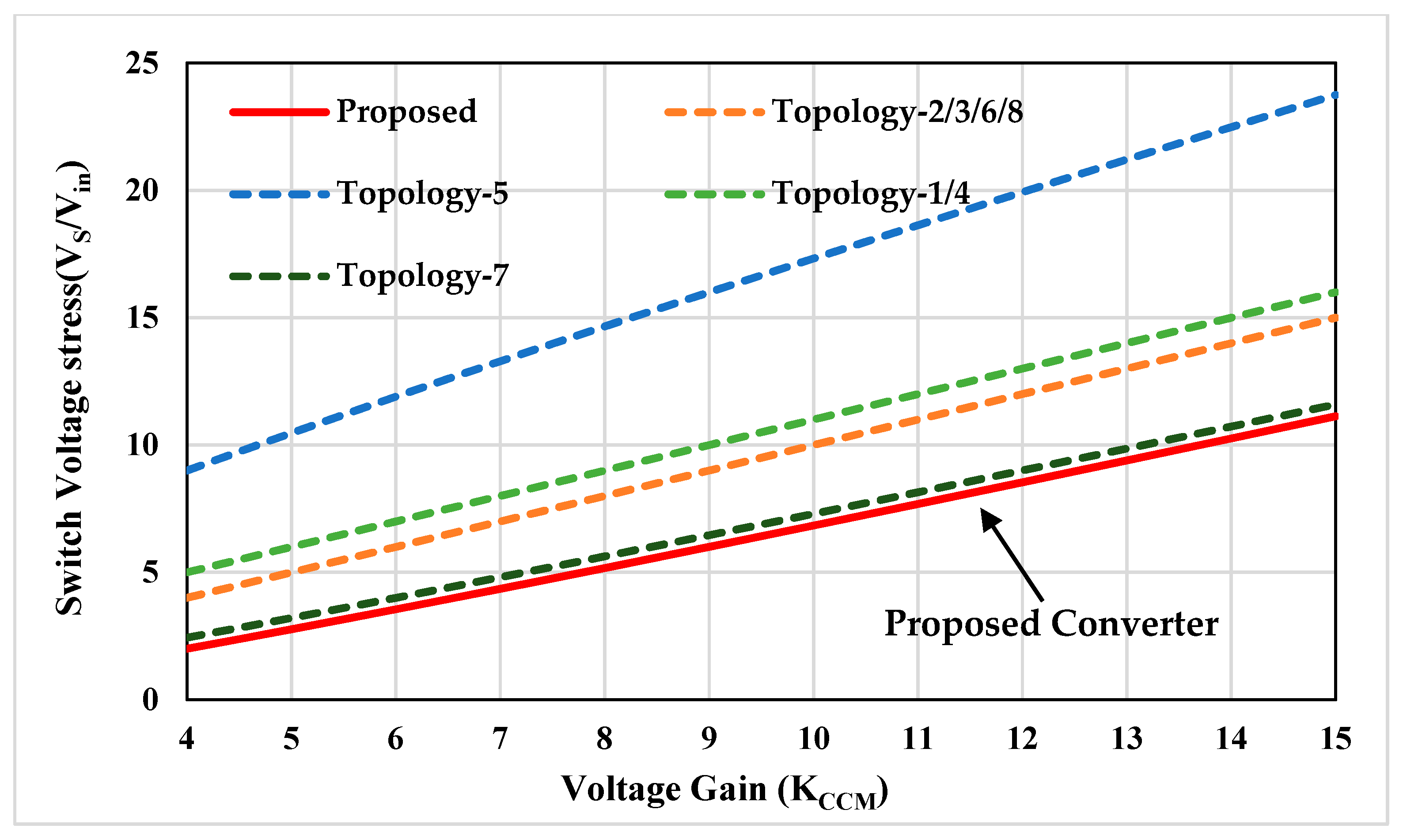
A detailed analysis of the proposed converter with similar non-isolated structures is carried out in this section. The comparison is based on voltage gain, voltage stress, and the number of components in the converters, as listed in
Table 1. Voltage gain is an important index to determine the performance of the converter. The voltage gain curve is shown in
Figure 12. The proposed converter can achieve the highest voltage gain till duty ratio (α) of 0.6 after α > 0.6; topologies two and eight are greater than the proposed converter. Topology nine uses coupled inductors to boost the voltage gain up to eight times (not shown in
Figure 12 and
Figure 13) because of the isolated category of DC-DC converters but has the maximum number of components compared to other converters listed in
Table 1.
The component counts of the proposed converter are less than topologies 1, 2, 5, and 8. Another important criterion is the voltage stress on the semiconductor devices. For this, a plot of normalized switch voltage stresses against the voltage gain of the proposed converter is shown in
Figure 13. The proposed converter has the least voltage stress on the switch, which is less than the output voltage. Topologies two and eight have higher voltage gain, but they have greater voltage stress than the proposed converter. Moreover, topologies two and eight both have a greater number of components than the proposed converter. Topologies 2, 3, 6, and 8 have voltage stress equal to the output voltage. The high voltage stress on the devices increases the chance of the failure of the devices, so devices with a higher rating will be required. The components with the higher rating will have increased costs and will deteriorate the efficiency of the converter due to high power loss. Topology 1 and topology 9 have a non-common ground structure, while other topologies, including the proposed converter, have a common ground structure.
The proposed topology can achieve higher gain with low stress on the components. The components with lower ratings will have low ON resistance, which will improve the overall efficiency of the converter. Moreover, the converter utilizes a single switch, so control is easy. The interleaved converter, presented in topology 9, utilizes two switches with a 180-degree phase difference. Further, the use of the coupled inductor makes the circuit complex. The proposed converter also provides a common ground structure between input and output, which mitigates electromagnetic interference problems. The volume of components is mainly decided by the magnetic components in the converter; the proposed converter uses only two inductors such as TQBC, so volume is low as compared to topologies 2, 3, 5, and 8 which utilizes three inductors. The use of more inductors makes the circuit bulkier.
6. Simulation Results at α = 0.4
In this section, simulation results of the proposed converter are discussed. The parameter values taken for simulation are presented in
Table 2. The simulation is carried out at an input voltage of 36 volts at a frequency of 50 kHz. Equivalent series resistance (ESR) of inductors and capacitors is also considered for the simulation on Piecewise Linear Electrical Circuit Simulation (PLECS) software. The duty cycle is maintained at 0.4.
Figure 14 shows the output voltage results of the proposed converter. The output voltage is obtained is 256 V, which is more than seven times the input voltage. The deviation obtained is due to a parasitic resistance drop in the proposed converter. The average current of inductors of L
1 and L
2 are 3.7 Ampere and 1.4 Ampere, as shown in
Figure 15. In the same figure, the ripple observed in the inductor current is very low, with a fixed duty ratio of 0.4. When the switch is OFF, it blocks the positive voltage equal to 159 V which is 62% of the V
o in
Figure 16. In the same figure, the average capacitor voltage V
C3 is 96 V.
Figure 17 presents the capacitor voltages of C
1 and C
2, equal to 36 V and 96 V, respectively. The simulation results obtained by using parameters mentioned in
Table 2 are in agreement with the theoretical results. It is to be mentioned that the converter is operated in the CCM mode.
7. Experimental Verification at α = 0.4
To verify the operating principles and boost the capability of the proposed converter, a hardware prototype of 200 W is developed and tested under laboratory conditions. The hardware prototype is shown in
Figure 18a and the hardware setup in
Figure 18b. The experimental waveforms are presented and demonstrated in this section.
The hardware parameters are the same as the simulation parameters given in
Table 3. The DC input supply is taken to be 10 V for the CCM mode operation of the proposed hardware prototype. The experimental gate pulse for the power MOSFET (SPW52N50C3) is 40 per cent.
Figure 19 captures the input (V
in) and output voltages (V
o) of the experimental prototype. The output voltage (V
O) obtained is 70 volts, where V
gs is the gate drive signal. When the MOSFET is ON, inductors L
1 and L
2 magnetize and the current through the inductors (I
L1 and I
L2) increases linearly. I
L1 increases from 0.15 Ampere to a peak value of 0.7 Ampere, whereas I
L2 increases from 1.0 Ampere to a peak value of 1.2 Ampere. The average current of inductors of L
1 and L
2 are 1.04 Ampere and 0.4 Ampere, as shown in
Figure 20. During the OFF state, the voltage across the switch is 40 V, which is less than V
O, as shown in
Figure 21. The capacitor voltages V
C1, V
C2, and V
C3 are 10 V, 26 V, and 26 V, respectively, captured in
Figure 20 and
Figure 21 with very low voltage ripple.
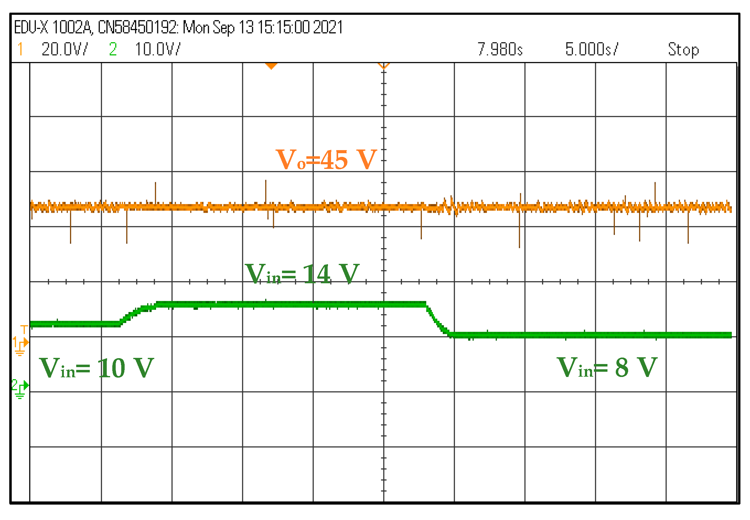
The closed-loop performance of the converter is illustrated in
Figure 22 and
Figure 23. The output voltage V
o is regulated at 45 V when the input voltage is varied from 10 volts to 14 V to 8 V. Similarly, when the load resistance is changed the output voltage should be held constant by the PI controller. As the load is changed from 300 Ω to 800 Ω, the output voltage is held constant at the set reference value of 60 V, as shown in
Figure 24. It shows that the PI controller is working satisfactorily. The values of proportional constant (K
p) and integral constant (K
i) for the PI controller are set to be 0.05 and 0.01 respectively. TMS320F28335 controller is used for implementation of closed-loop control.
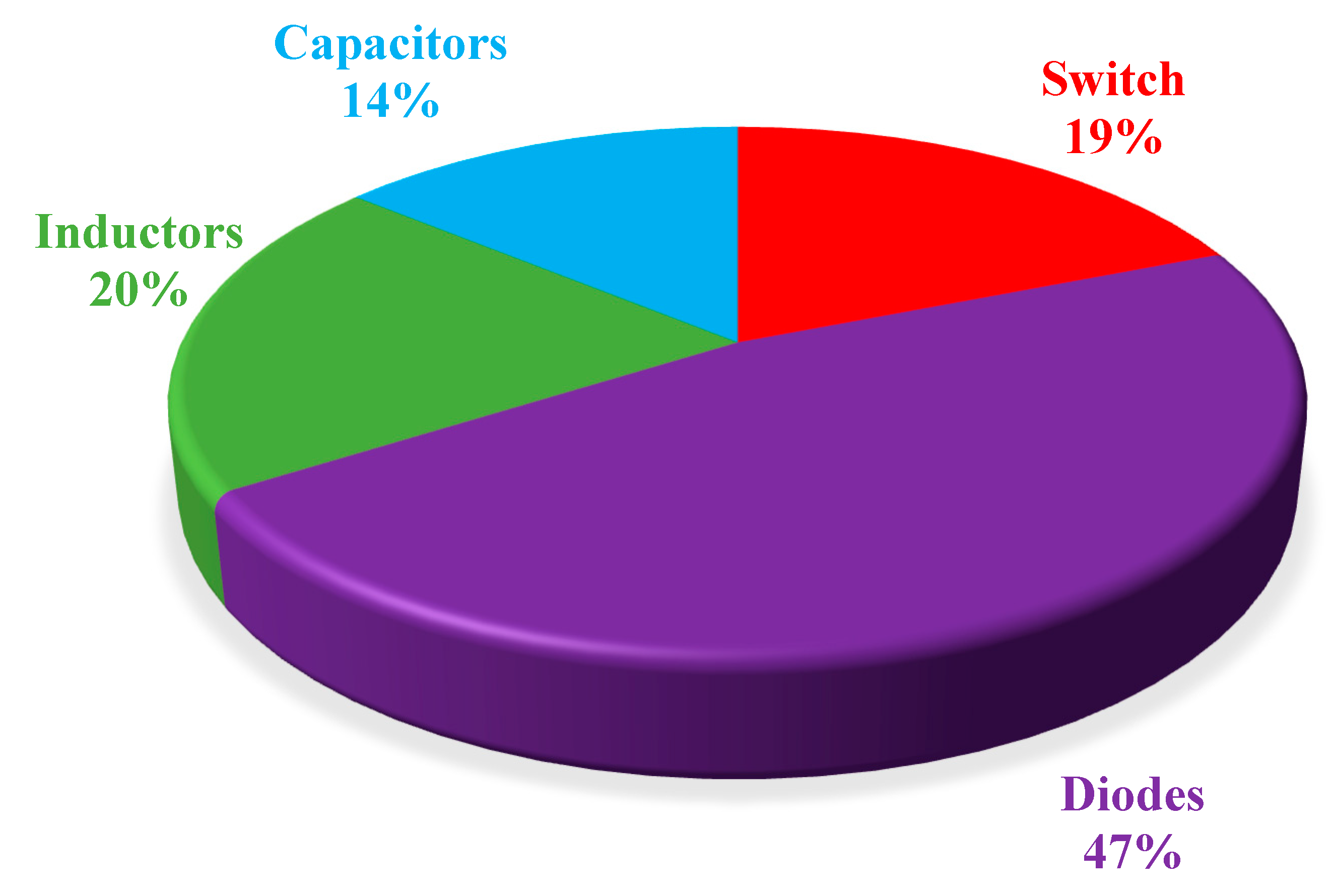
The efficiency at different power levels is shown in
Figure 24. It can be seen from the plot that for a constant output power as the voltage increased from 10 V to 20 V, the efficiency of the converter increased. This is because to achieve the same power level, the current decreases with the increase in output voltage. As a result, the conduction losses in the converter decreases and efficiency increases. The percentage losses in the components as calculated from the PLECS software by incorporating the real loss values from the datasheet of different component. 47% of the total loss, occurs in diodes, as shown in
Figure 25. The switch losses are around 19%. Losses in the inductors and capacitors are found to be 20% and 14% respectively. The diode losses can be reduced by the selection of diodes with a low value of parasitic resistances. The capacitor ESR depends on the frequency and hence capacitor losses increase with an increase in frequency.


 ,
, 


