Article

Design and Implementation of a High Step-Up DC-DC Converter Based on the Conventional Boost and Buck-Boost Converters with High Value of the Efficiency Suitable for Renewable Application

1
Key Laboratory of Power System Intelligent Dispatch and Control, School of Electrical Engineering, Shandong University, Ministry of Education, Jinan 250061, China
2
School of Electrical, Computer and Telecommunications Engineering (SECTE), Faculty of Engineering and Information Sciences, University of Wollongong, Wollongong, NSW 2522, Australia
3
Faculty of Electrical Engineering, Shahid Beheshti University, Tehran 1983969411, Iran
*
Authors to whom correspondence should be addressed.
Sustainability 2021, 13(19), 10699; https://doi.org/10.3390/su131910699
Submission received: 1 September 2021 / Revised: 17 September 2021 / Accepted: 18 September 2021 / Published: 26 September 2021

Abstract

:
This paper introduces a novel topology of the proposed converter that has these merits: (i) the topology of the converter is based on conventional boost and buck-boost converters, which has caused its simplicity; (ii) the voltage gain of the converter has provided higher values by the lower value of the duty cycle; (iii) due to the use of high-efficiency conventional topologies in its structure, the efficiency of the converter keeps its high value for a great interval of duty cycle; (iv) besides the increase of the voltage gain, the current/voltage stresses of the semiconductors have been kept low; (v) the continuous input current of this converter reduces the current stress of the capacitor in the input filter. It is worth noting that the proposed converter has been discussed in both ideal and non-ideal modes. Moreover, the operation of the converter has been discussed in both continuous/discontinuous current modes. The advantages of the converter have been compared with recently suggested converters. In addition, the different features of the converter have been discussed for different conditions. In the small-signal analysis, the appropriate compensator has been designed. Finally, the simulation and experimental results have been reported for 90 W output power, 90 V output voltage, 3-times voltage gain, and 100 kHz switching frequency.

1. Introduction

Renewable applications require a high efficiency, high gain, and low volume converter. The buck-boost and boost converters are conventional converters that are capable of increasing their input voltage [1]. These converters are appropriate for high-efficiency applications. In addition, the simplicity of their topology has caused their popularity as well as their efficiency. To provide high values of the voltage gain, the duty cycle’s percentage has to approach 100 percent. However, such a high value of the duty cycle results in a dramatic switch loss besides the high value of the semiconductors’ current/voltage stresses [2,3,4]. Moreover, the resulted voltage gain is not the same as the prediction of their voltage gain equation. According to Figure 1a, an increase in the duty cycle can not always increase the voltage gain. Moreover, the very close value of the duty cycle to unity results in a decreasing behavior of the voltage gain. Furthermore, the output power is the other effective factor. Based on Figure 1b,c, the increase of the output power besides a constant voltage decreases the maximum voltage gain. Moreover, an increase in the output power decreases the corresponding interval of rising behavior of the voltage gain. The high duty cycle has a destroying effect on efficiency. As has been presented in Figure 1d, the high value of the duty cycle provides poor values of efficiency. Consequently, providing a high value of the voltage gain by the low value of the duty cycle is not possible [5,6,7,8].
Employing high-frequency transformers can be a solution to increase the voltage gain [9]. In other words, the turn ratio of coils can be step-up isolated from the input source. Therefore, the load is isolated from the input source. Therefore, the load will be protected from happening faults on the input side [10]. However, the switches of this kind of converter suffer from high current stresses due to the current inertia of the leakage inductance [11]. Such a shortage can be solved by applying snubber circuits which increase the number of elements [12]. The shortage of transformer base converters does not stop here and EMI is another one. Furthermore, the high volume, mass, and cost of this kind of converter is another disadvantage [13]. Consequently, the use of this kind of converter is not recommended for applications that do not require the isolation of the load from the input source. Switch-capacitor topologies are the solution for increasing the voltage gain [14]. In this kind of converters, switching of switches copies the voltage in parallel connected capacitors and then, the series connection of capacitors results in a high output voltage. However, the parallel switching of capacitors causes inrush currents that the semiconductors suffer from the resulted current stress [8,11,12,14].
The quadratic DC-DC converters are another solution to increase the voltage gain. These topologies can be easily made by cascading or restructuring conventional converters. In [15,16,17,18,19,20,21,22,23,24,25,26], recently suggested quadratic DC-DC converters have been reported. The reported converters of [15,16,17,18,19,20,21,22,23,24,25,26] can be divided into three groups based on the equation of their voltage gain. The voltage gain of [15,16,17,18,19,20,21] is 1, while the percentage of the duty cycle becomes 50 percent. Moreover, the output voltage is twice the input source in [22,23,24,25]. Furthermore, a 50 percent duty cycle increases the input voltage to three times more than itself. The quadratic buck-boost converter of [15] has used three inductors. In other words, its dimension has been increased. Moreover, besides the high number of the inductors and low value of the resulted voltage gain, the conduction loss of the inductors has a high value. Moreover, the corresponding losses of the switches and diodes are high as well as the voltage stress of the semiconductors is dramatically high. The proposed converter in [16] has been made up of a simple cascaded two buck-boost converter. In comparison with [15], it has two inductors. Unlike the presented converter in [15] the input current is discontinuous. The voltage stress of the second switch and diode is higher than the resulted voltage level of the output. Moreover, the switch and diode losses have become high. The suggested topology in [17] has achieved a continuous input/output current. However, the semiconductors suffer from high voltage/current stresses. Moreover, the use of three inductors has increased its volume. Furthermore, the different kinds of losses are high and undesired. Same as the topology of [17], the represented topology in [18] has continuous input/output currents. The topology of this converter has employed PNP and NPN MOSFETs. Such different kinds of switches result in different driving circuits. Moreover, its volume has been increased due to its three inductors. Furthermore, the corresponding loss of the inductors has been increased. Additionally, the second switch and diode of this converter suffer from high voltage stress. The reported topology in [19] is a simple cascade of two buck-boost converters. The same as the converters of [16,18], PNP and NPN MOSFETs have been used in this topology. It is worth noting that, due to the use of buck-boost converters in its topology, the input current is discontinuous. Additionally, the second switch and diode experience a voltage higher than the output voltage of the converter. In comparison with [16], the corresponding loss of the inductors is high. Other combinations of the buck-boost converter have been reported in [20,21]. It is worth noting that the combination of the conventional converters has been done in a way that has caused the continuity of the input current. It is good to mention that two different driver circuits have to be used in the suggested converters of [20,21] due to the use of PNP and NPN MOSFETs together. The proposed topology in [21] has a lower inductor/switch loss in comparison with [20]. Additionally, the semiconductor in these two topologies suffers from high voltage stress. Another type of quadratic converter with continuous input current has been reported in [22]. It is worth noting that the topology of this converter is in a way that causes high voltage stress on the switches. Moreover, the corresponding losses of the switches and diodes have become increased. Furthermore, the first switch suffers from high current stress. The reported topology in [23] has the same number of components as in [22]. In addition, three inductors have made it high-measured. Moreover, the voltage stress of the second switch and diode has been increased dramatically. The suggested topology in [24,25,26] has the same component count. Most of the semiconductors in these topologies suffer from high current/voltage stress. Besides the low inductor and switch losses in [25,26], their diode loss is high. It is good to mention that all types of losses in [24] are not desired.
The quadratic converters increase the degree of the relation of the voltage gain from one to two. Consequently, the provided voltage gain by the conventional converters becomes squared. However, such a modified form increases the degree of the relation of the average current of the inductors. As a result, the decrease of efficiency concerning the increase of the duty cycle takes place rapidly. In other words, the efficiency loses its high value in the shorter interval of the duty cycle. According to Figure 1d, the efficiency of the conventional converters remains more than 90 percent while the duty cycle varies from 0 to 80 percent. However, this interval of the duty cycle gets shorter. Therefore, the conventional topologies with high efficiency have to be combined with themselves besides the increase of the voltage gain and without the increase of the loss intensity. In this paper, the conventional boost and buck-boost converters are combined so that their output voltages are summed with each other. Consequently, the voltage gain has been increased without any difference in the losses of each circuit component. Additionally, the proposed converter is capable of providing a higher value of efficiency for a wide span of the duty cycle. This concept states the better functioning of this converter in comparison with the suggested converters of [15,16,17,18,19,20,21,22,23,24,25,26]. It is worth noting that the detailed expressions have been reported in the fourth and fifth sections. Due to the use of the conventional topologies in the presented converter, its simplicity is a brilliant feature. The higher value of the voltage gain besides the high efficiency, low voltage/current stress of the semiconductors, and use of a low value of the duty cycle is a remarkable point in comparison with [15,16,17,18,19,20,21,22,23,24,25,26] which has been deeply explained in the fourth and fifth sections. The detailed expression of the converter and its operation parameters have been discussed in the second section. In the third section, the operation of the converter in the discontinuous current mode (DCM) has been explained. The appropriate voltage gain of the converter in the non-ideal mode of the circuit components has been extracted and compared with the recently suggested converters of [15,16,17,18,19,20,21,22,23,24,25,26] in the fourth section and the better behavior of the converter for a longer interval of the duty cycle has been discussed. The fifth section is devoted to the discussion of efficiency. Different parameters such as current/voltage stress of the semiconductors, different kinds of losses, topological features, and storage energy of the converters have been compared and remarkable points of the proposed topology have been discussed in the sixth section. The small-signal analysis has been done in the seventh section. Finally, the simulation and experimental results have been extracted and discussed in the eighth section.

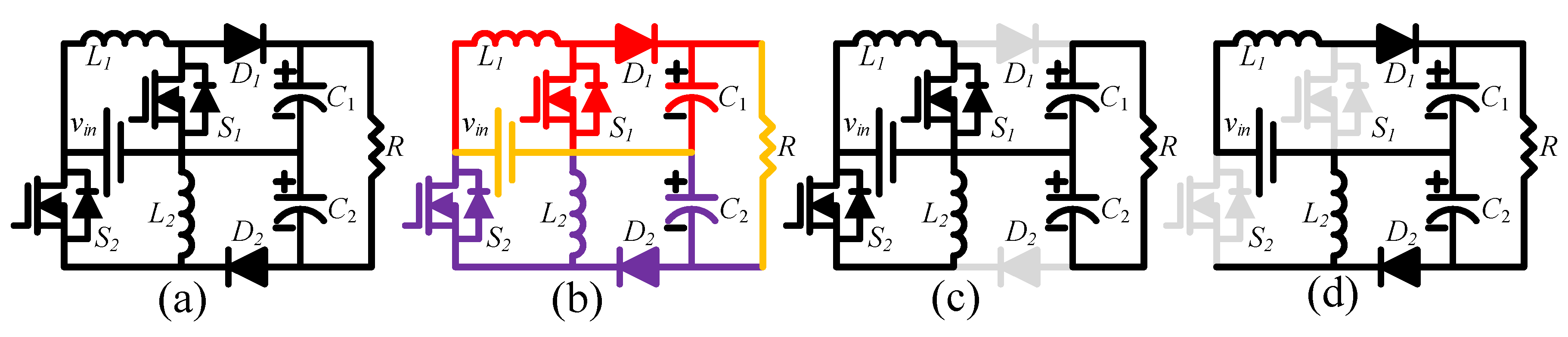
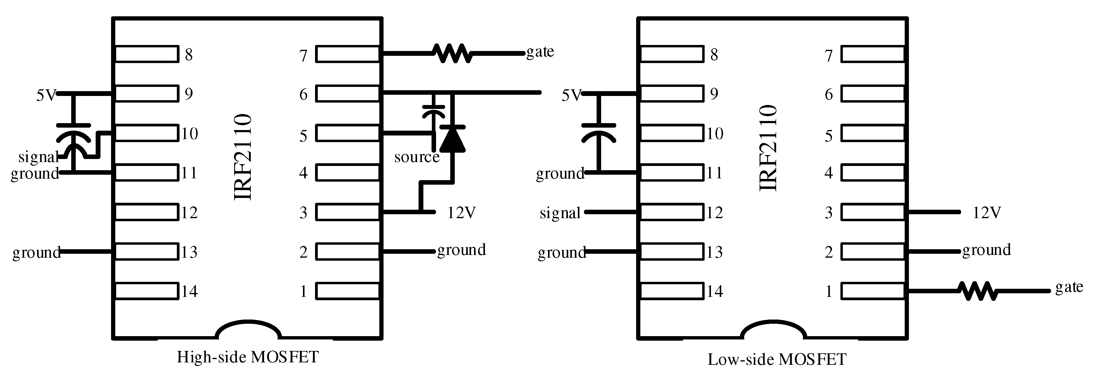
2. Proposed Converter

The topology of the proposed converter has been presented in Figure 2a. According to Figure 2b, the conventional boost and buck-boost converters have composed the topology. The same semiconductor-based components are activated and inactivated synchronously. It is worth noting that, during the activation of the switches, the diodes are OFF. To discuss this converter in this section, some assumptions have to be considered as follows:
  • The operation of the converter takes place in the continuous conduction mode (CCM).
  • All the circuit components are ideal and their parasitic components are neglected.
  • The capacitors are large enough to keep their voltage constant.
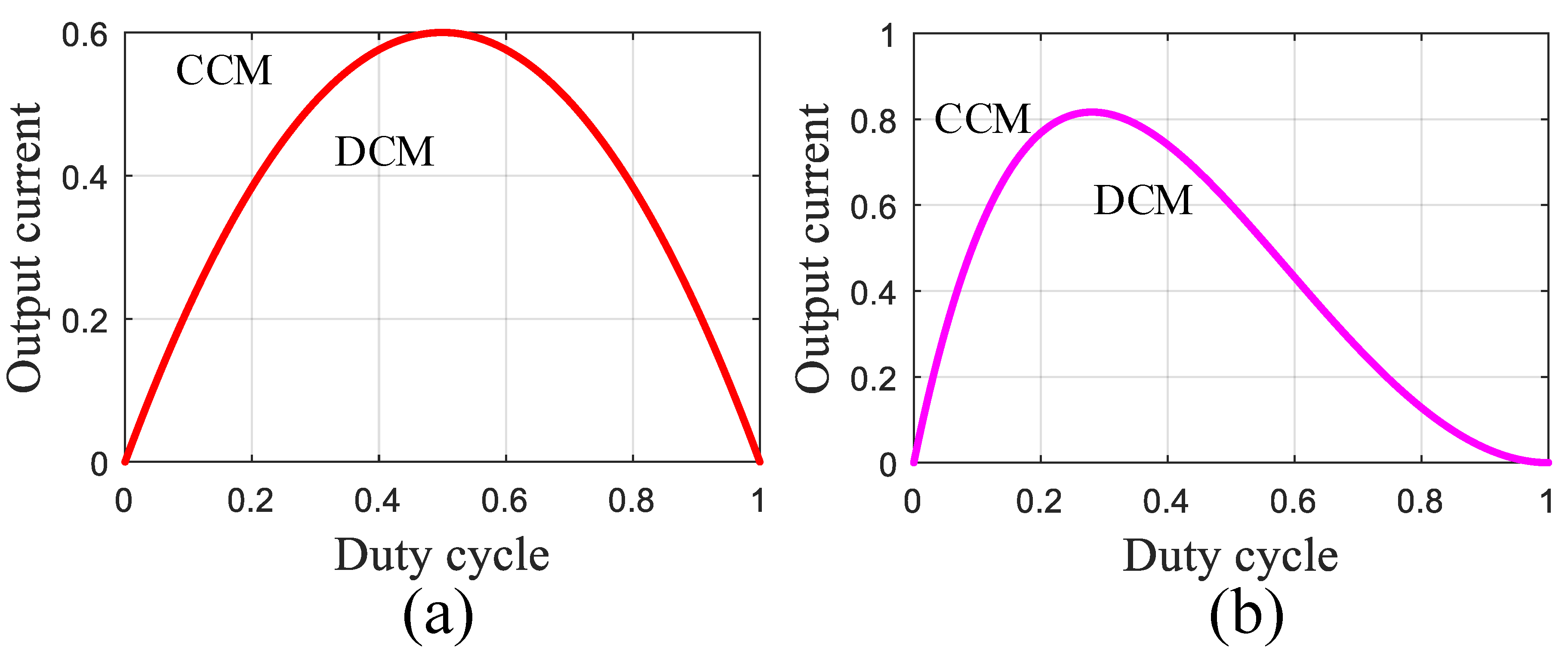
The first operation mode of the converter is started by activation of both switches. According to Figure 2c, the diodes are in their reverse biased. It is worth noting the inductors are magnetized due to their positive voltage as well as the capacitors are discharged due to their negative current. The inactivation of switches and the activation of the diodes start the second operation mode. The equivalent circuit of the converter in this mode has been illustrated in Figure 2d. The inductors’ voltage and capacitors’ current during both operation modes are (1):
L 1 d i L 1 d t = D v i n + ( 1 D ) ( v i n v c 1 ) L 2 d i L 2 d t = D v i n + ( 1 D ) ( v c 2 ) C 1 d v c 1 d t = D ( V o R ) + ( 1 D ) ( i L 1 V o R ) C 2 d v c 2 d t = D ( V o R ) + ( 1 D ) ( i L 2 V o R )
According to the voltage second balance, the inductors’ average voltage is zero as well as the current second balance concludes the zero average currents of capacitors. Therefore, based on Equation (1), the average voltage of the capacitors and average current of inductors can be expressed as (2):
V C 1 = V i n 1 D , V C 2 = V i n D 1 D , V C o = 1 + D 1 D V i n I L 1 = I L 2 = 1 1 D V o R , I i n = 1 + D 1 D V o R
The voltage stress of the semiconductors can be expressed according to their inactivation mode as well as their current stress can be expressed according to their activation mode as (3):
V S 1 = V S 2 = V D 1 = V D 2 = V i n 1 D I S 1 = I S 2 = D 1 D V o R , I D 1 = I D 2 = V o R
The simplified relation of the inductors’ current ripple can be expressed according to their applied voltage during the operation modes. Moreover, the simplified relation of the capacitors’ voltage ripple can be expressed according to the crossing currents through them as (4):
Δ i L 1 = Δ i L 2 = D V i n L 1 , 2 f s , Δ v c 1 = Δ v c 2 = D I o C 1 , 2 f s

3. DCM Mode

In the second section, the extracted relation of voltage gain has been expressed for the continuous current mode. Another time interval exists when both the switches and diodes are inactive in the discontinuous current mode. The duty cycle represents the ratio of the ON-time over the entire period and is denoted by D. Moreover, the ratio of the time interval of ON mode of diodes over the whole period has been illustrated by D 1 . The time interval of the OFF mode of all semiconductors over the whole period has been illustrated by D 2 . The relation of D, D 1 , and D 2 is as below:
D + D 1 + D 2 = 1
Based on the mentioned concepts, the voltage gain of the proposed converter in DCM, has been expressed as below:
V o V i n = 2 D + D 1 D 1
The operation of the converter in DCM or CCM depends on the value of the inductors and their average currents. To ensure the proper operation of the proposed converter in CCM, the boundary value of the inductors has been expressed as (7):
L 1 > R D ( 1 D ) 2 f s ( 1 + D ) , L 2 > R D ( 1 D ) 2 f s ( 1 + D )
According to Figure 3a,b, the operation of the converter in CCM or DCM regions has been presented based on the value of the output current and duty cycle. It is worth noting that Figure 3a has been extracted for a constant output voltage as well as Figure 3b has been extracted for a constant input voltage.

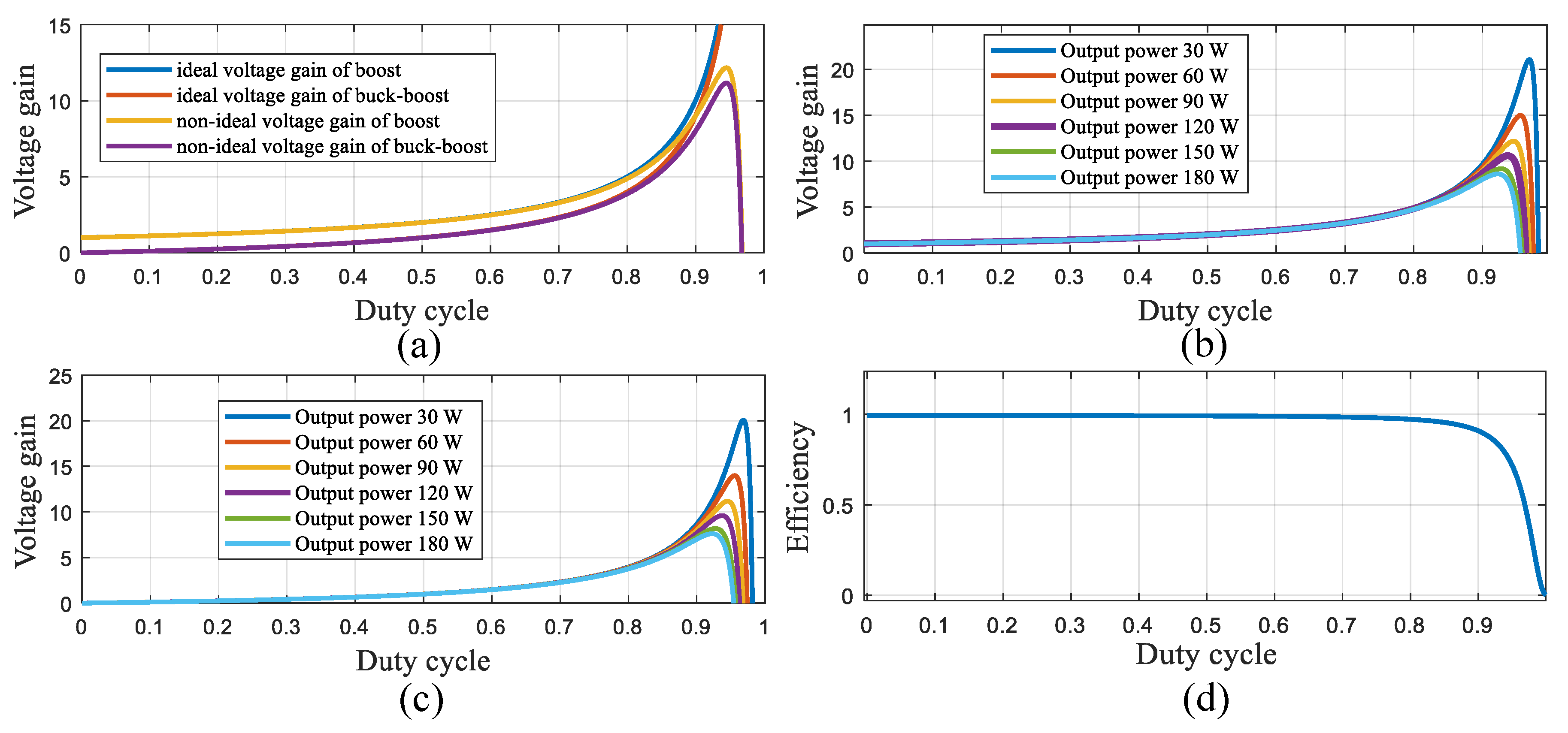
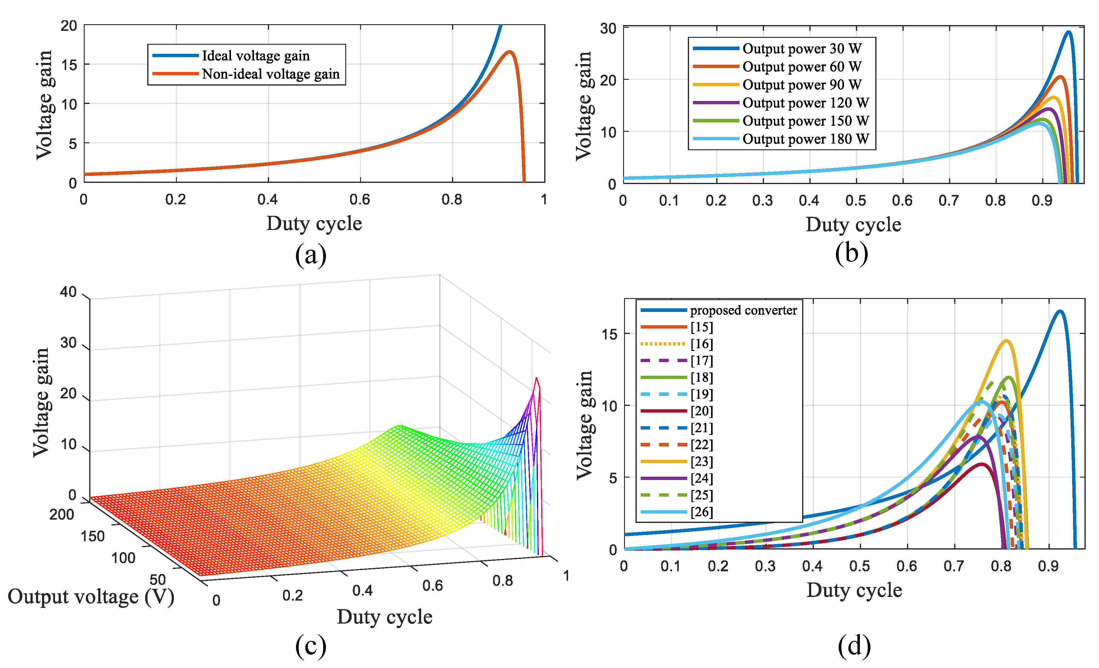
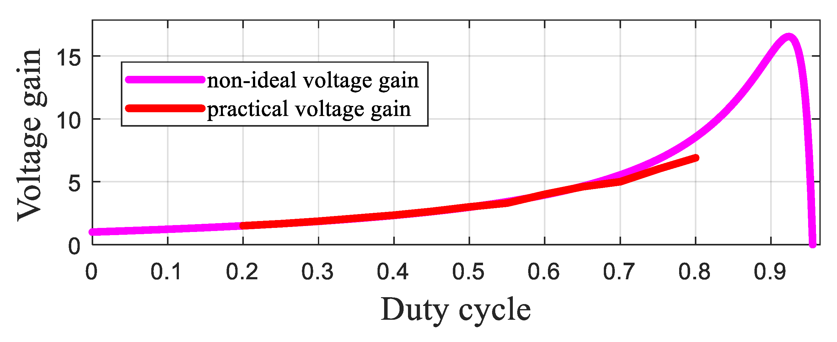
4. Non-Ideal Voltage Gain

The Relation of the Non-Ideal Voltage Gain

In the second section, the ideal mode of the circuit components has been assumed and the voltage gain was extracted. To explain the real behavior of the proposed converter with the mathematical relations, the series resistance of the inductors, and switches besides the voltage drop of the diodes have been considered and the non-ideal voltage gain has been extracted as below:
C C M : V o V i n = 1 + D 1 D 1 r L R 2 ( 1 D ) 2 r D S R 2 D ( 1 D ) 2 r D R 2 1 D D C M : V o V i n = D 1 + 2 D D 1 1 r L R ( 2 ( D 1 + D D 1 ) 2 ) r s R ( 2 D ( D + D 1 ) D 1 2 ) r D R ( 2 ( D 1 + D ) D 1 )
where the r L , r S D , and r D refer to equivalent series resistance of the inductors, equivalent series resistance of the switches, and voltage drop of the diodes respectively.
According to Equation (8), the voltage gain of the converter in both ideal and non-ideal modes has been compared in Figure 4a. It is worth noting that the ideal and non-ideal voltage gains behave as same as each other, while the duty cycle varies from 0 to 80 percent. Moreover, the maximum voltage gain has occurred at the 93 percent duty cycle. It is worth noting that the behavior of the voltage gain in the non-ideal mode of components depends on the quality of the circuit elements and output power. According to Figure 4b, the increase of the output power besides a constant output voltage decreases the maximum value of the voltage gain as well as its corresponding duty cycle. In Figure 4c, the behavior of the voltage gain has been presented varying both duty cycle and output power. It can be understood that the resulted voltage gain is the same at lower values of the duty cycle for all output power values. In addition, increasing the duty cycle to higher values causes more differences in the corresponding voltage gain of various output powers.
In Figure 4d, the voltage gain of the proposed converter and [15,16,17,18,19,20,21,22,23,24,25,26] have been compared in their non-ideal mode. While the duty cycle varies from 0 to 50 percent, the voltage gain of the proposed topology provides higher values in comparison with [15,16,17,18,19,20,21,22,23,24,25,26]. In addition, while the duty cycle varies from 50 to 60 percent, the voltage gain of the suggested converter is higher than [15,16,17,18,19,20,21,22,23,24,25]. Moreover, the increase of the duty cycle from 60 to 7 percent, makes the voltage gain of this converter higher than [15,16,17,18,19,20,21]. It is worth noting that, while the duty cycle varies from 70 percent to 85 percent, the maximum value of the voltage gain takes place for all converters of [15,16,17,18,19,20,21,22,23,24,25,26]. Unlike the converters of [15,16,17,18,19,20,21,22,23,24,25,26], the voltage gain of the converter keeps its rising behavior until the percentage of the duty cycle becomes 93 percent.

5. Efficiency

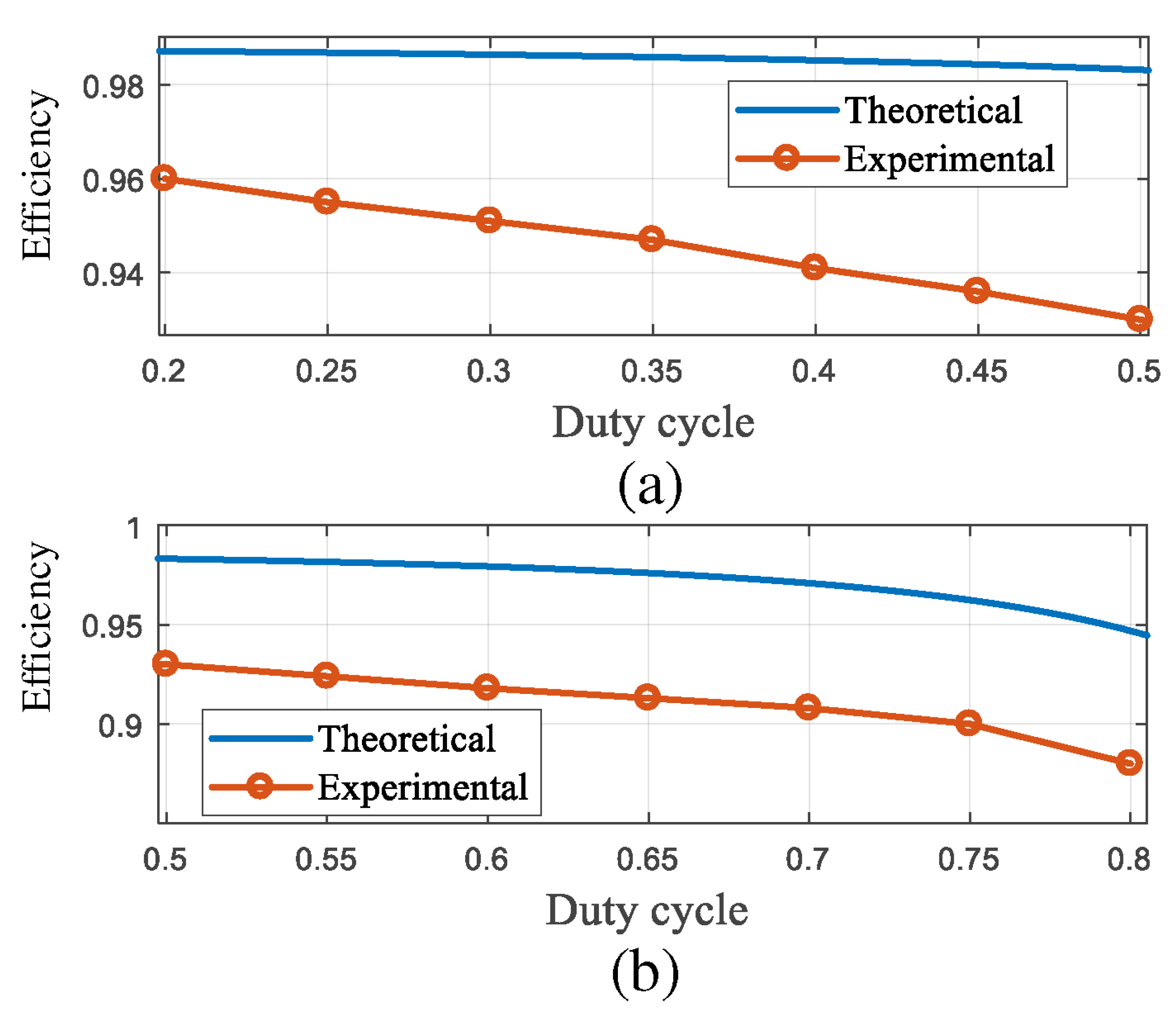
5.1. Mathematical Relations of the Efficiency

To define the efficiency of the proposed converter, the inductor loss, the switch loss, and the diode loss have been expressed, and magnetic and eddy current loss of inductors have been ignored. In the expressed relations of the power losses, r L , r S D , v D F , t o f f , R, and P o refer to the resistance of the inductor, the dynamic resistance of the switch, the threshold voltage of the diodes, the turn OFF delay time, load, and the output power, respectively.
The inductor loss of the proposed converter has been expressed as below:
P L = n = 1 2 r L n I 2 r m s n = r L 1 + r L 2 ( 1 D ) 2 P o R
The conduction loss of the switches can be expressed as below:
P S C = n = 1 2 r D S n I 2 S n , r m s = ( r D S 1 + r D S 2 ) D ( 1 D ) 2 P o R
The switching loss of the switches has been expressed as below:
P S S = n = 1 2 1 2 I S n V S n t o f f n f s = D P o f s ( t o f f 1 + t o f f 2 ) 2 ( 1 D ) 2
The diode loss of the proposed converter has been written as below:
P D = n = 1 2 V D F n I D n = ( V D F 1 + V D F 2 ) I o
The efficiency of the proposed converter can be expressed as below:
P o P o + P L + P D + P S C + P S S
According to the expressed equations of losses and efficiency, the quality of the circuit components and output power affect the efficiency value. In Figure 5a,b, the efficiency of the converter has been extracted for the different output powers. According to Figure 5a, the efficiency of the converter is higher than 97.5 percent for 30 W to 180 W output power and the duty cycle varies from 0 to 50 percent. In addition, according to Figure 5b, the efficiency is more than 95 percent while the duty cycle varies from 50 to 70 percent as well as the output power varies from 30 W to 180 W. Moreover, the efficiency of the converter remains more than 90 percent for all the mentioned output powers while the duty cycle is lower than 80 percent. Furthermore, the increase of the duty cycle from 80 percent to 85 percent makes the corresponding efficiency of 120 W to 180 W output power lower than 90 percent. It is worth mentioning that the 3-dimensional figure of the efficiency has been plotted for the varying output power and duty cycle in Figure 5c.
In Figure 5d,e, the efficiency of the proposed converters and the suggested converters in [15,16,17,18,19,20,21,22,23,24,25,26] has been compared. According to Figure 5d, while the duty cycle varies from 0 to 50 percent, the variation of the efficiency is lower than 0.5 percent in the proposed converter. However, the mentioned variation is more than 2 percent. In addition, the efficiency of the proposed converter is approximately constant and equals 98.9 percent. Moreover, the efficiency of the introduced converter is 98.5 percent while the percentage of the duty cycle is 50 percent. According to Figure 5e, while the duty cycle varies from 50 to 85 percent, the efficiency of the converter is still more than 90 percent. However, the suggested converters in [15,16,17,18,19,20,21,22,23,24,25,26] have the same condition while the duty cycle is lower than 60 percent. Consequently, the proposed converter can provide higher voltage gain by the close value of the duty cycle to unity besides the high value of the efficiency.

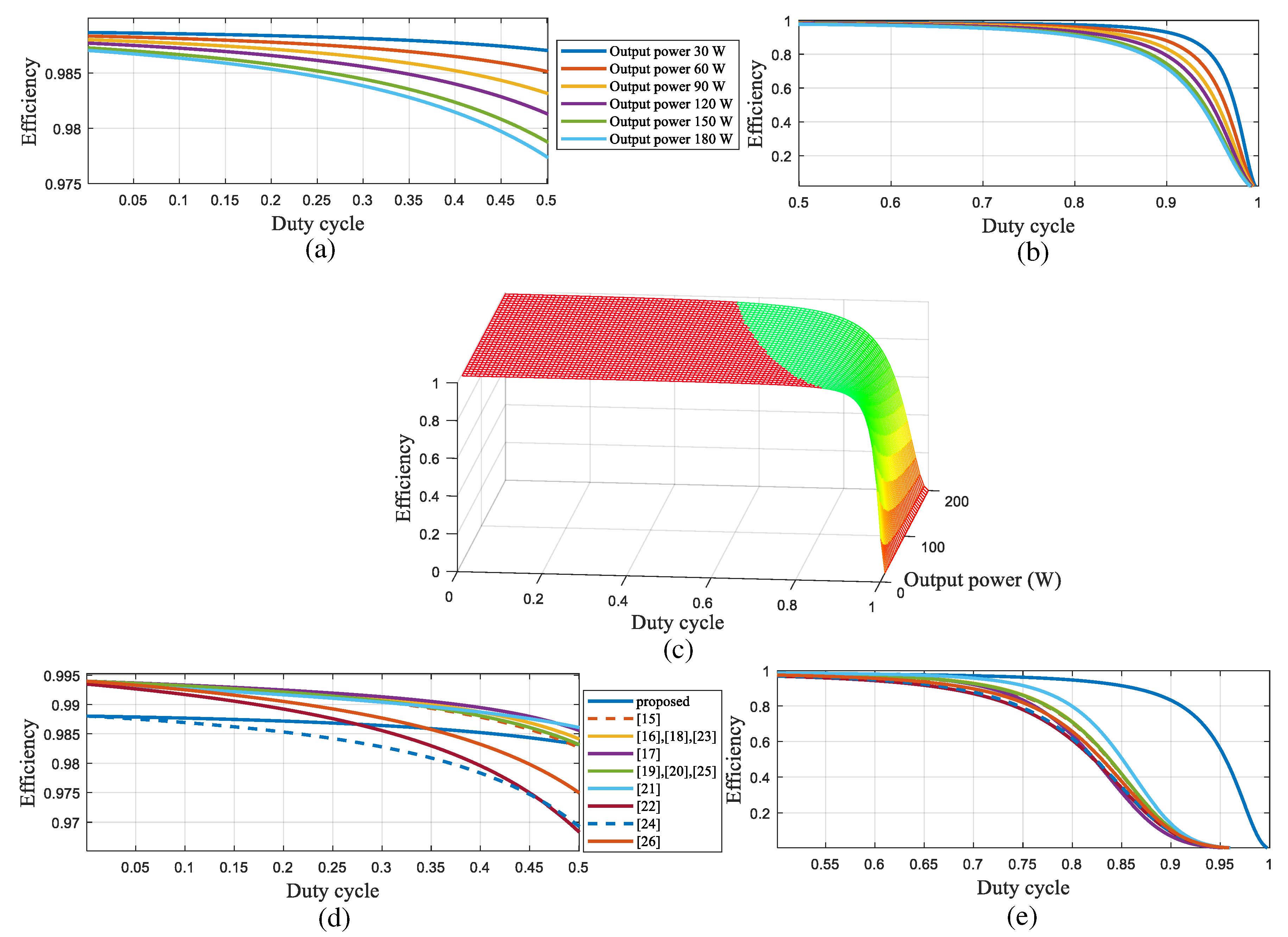
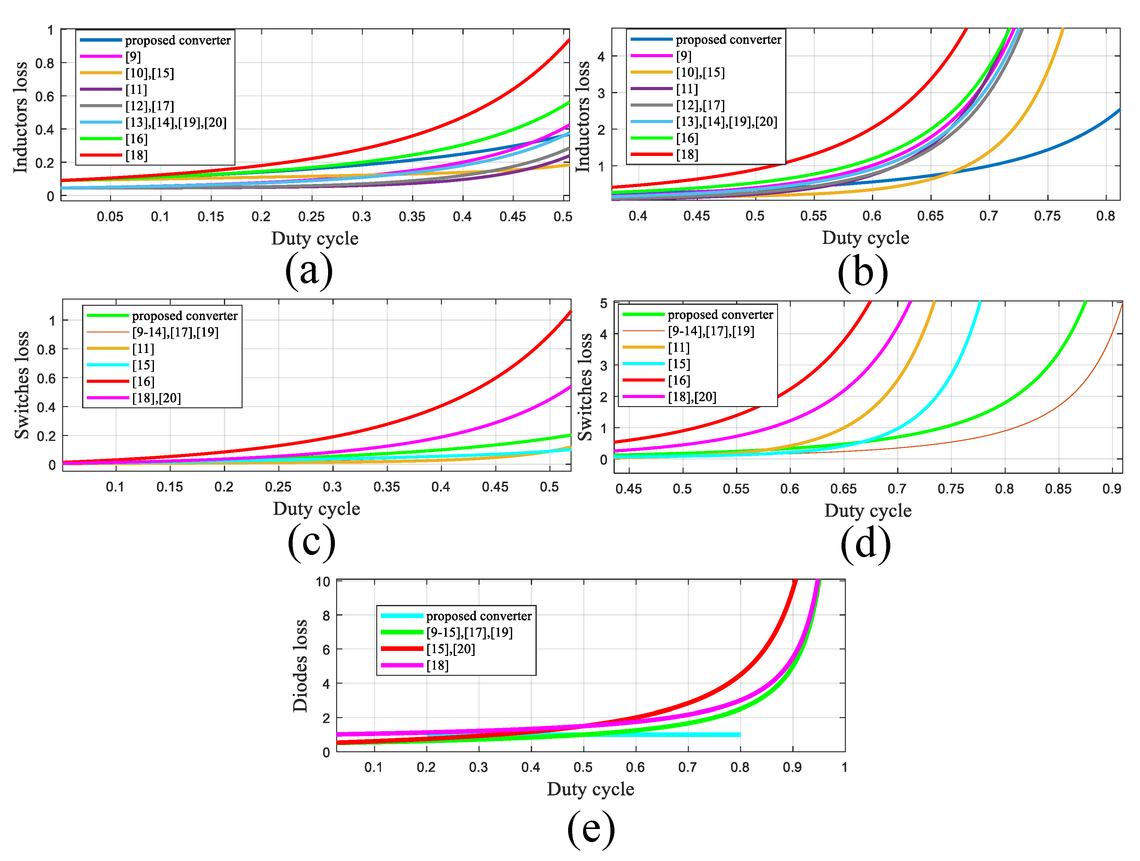
5.2. Comparison of the Various Losses of the Proposed Converter with the Other Step-Up Topologies While the Duty Cycle Is Varying and Output Power Is 90 W

In Figure 6a,b, the inductor loss of the proposed converter has been compared with the inductor loss of [15,16,17,18,19,20,21,22,23,24,25,26]. In Figure 6a, the duty cycle varies from 0 to 50 percent, and in Figure 6b, the duty cycle varies from 40 percent to 80 percent. In Figure 6a, the inductor loss of the proposed converter is lower than the inductor loss of the converters of [22,24], higher than the remaining converters, and varies from 0.1 W to 0.4 W. In Figure 6b, while the duty cycle varies from 50 percent to 80 percent, the inductor loss of the proposed converter is lower than all the mentioned converters except for the converters of [16,21]. It is worth noting that the inductor loss of the proposed converter becomes lower than the mentioned converters of [16,21] while the duty cycle varies from 67 percent to 80 percent.
In Figure 6c,d, the switching loss of the proposed converter has been compared with the mentioned converters of [15,16,17,18,19,20,21,22,23,24,25,26] while the duty cycle varies from 0 to 50 percent and 45 percent to 90 percent respectively. As can be understood from Figure 6c, the switching loss of the proposed converter is lower than the mentioned converters of [22,24,26]. Moreover, it can be understood from Figure 6d they the switching loss of the proposed converter is lower than the mentioned converters of [17,21,22,24,26].
In Figure 6e, the diode loss of the proposed converter has been compared with the proposed converters of [15,16,17,18,19,20,21,22,23,24,25,26]. As can be understood, while the duty cycle varies from 0 to 50 percent, the diode loss of the proposed converter is lower than the mentioned converter of [24] and while the duty cycle varies from 50 percent to 80 percent, the diode loss of the proposed converter is lower than the mentioned converters of [15,16,17,18,19,20,21,22,23,24,25,26].

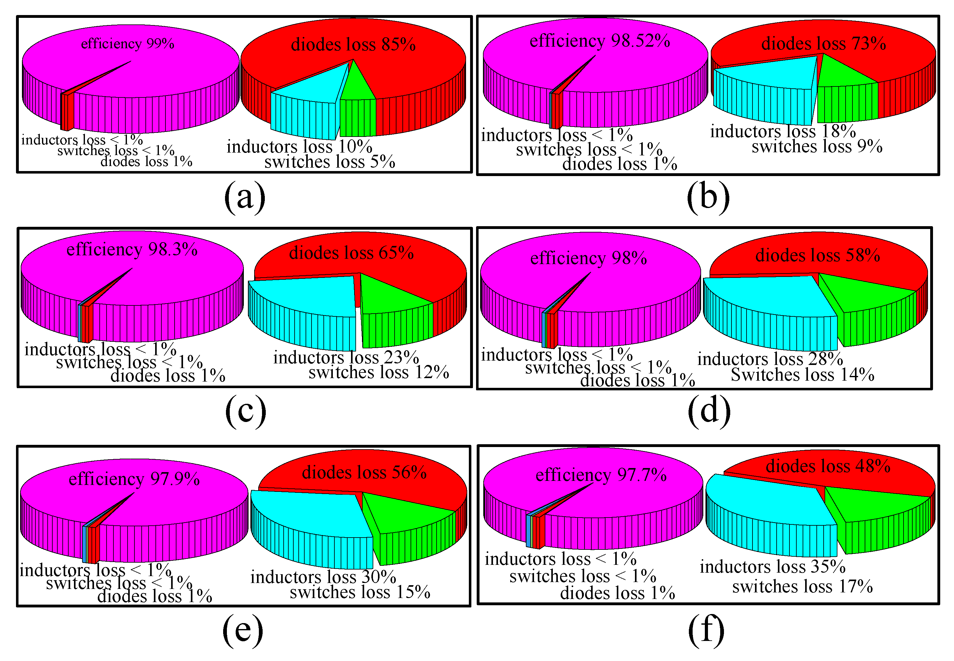
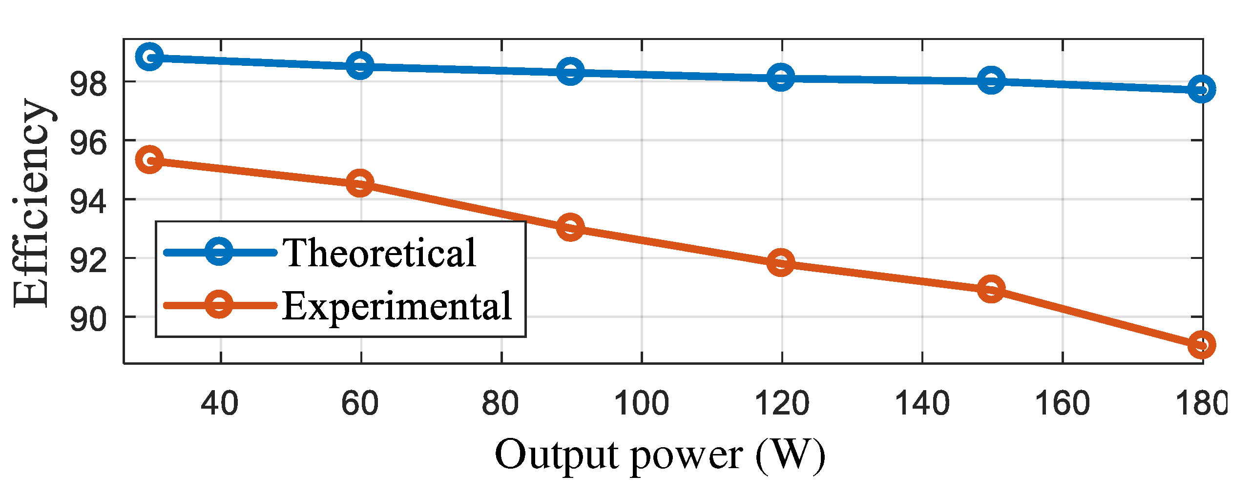
5.3. The Efficiency and Losses of the Proposed Converter for the Different Vales of the Output Power

In Figure 7a–f, the percentage of the efficiency and the different kinds of loss have been illustrated for the output power of 30 W, 60 W, 90 W, 120 W, 150 W, and 180 W. It is worth noting the percentage of the duty cycle is 50 percent. As can be understood, the major loss is diode loss. Moreover, an increase in the output power leads to an increase in the inductor loss to more than twice the switching loss. Furthermore, an increase of output power to more than 150 W concludes the higher value of the summation of the inductor and switch loss in comparison with the diode loss. It is worth noting that in all the mentioned output powers, the efficiency is more than 97 percent.

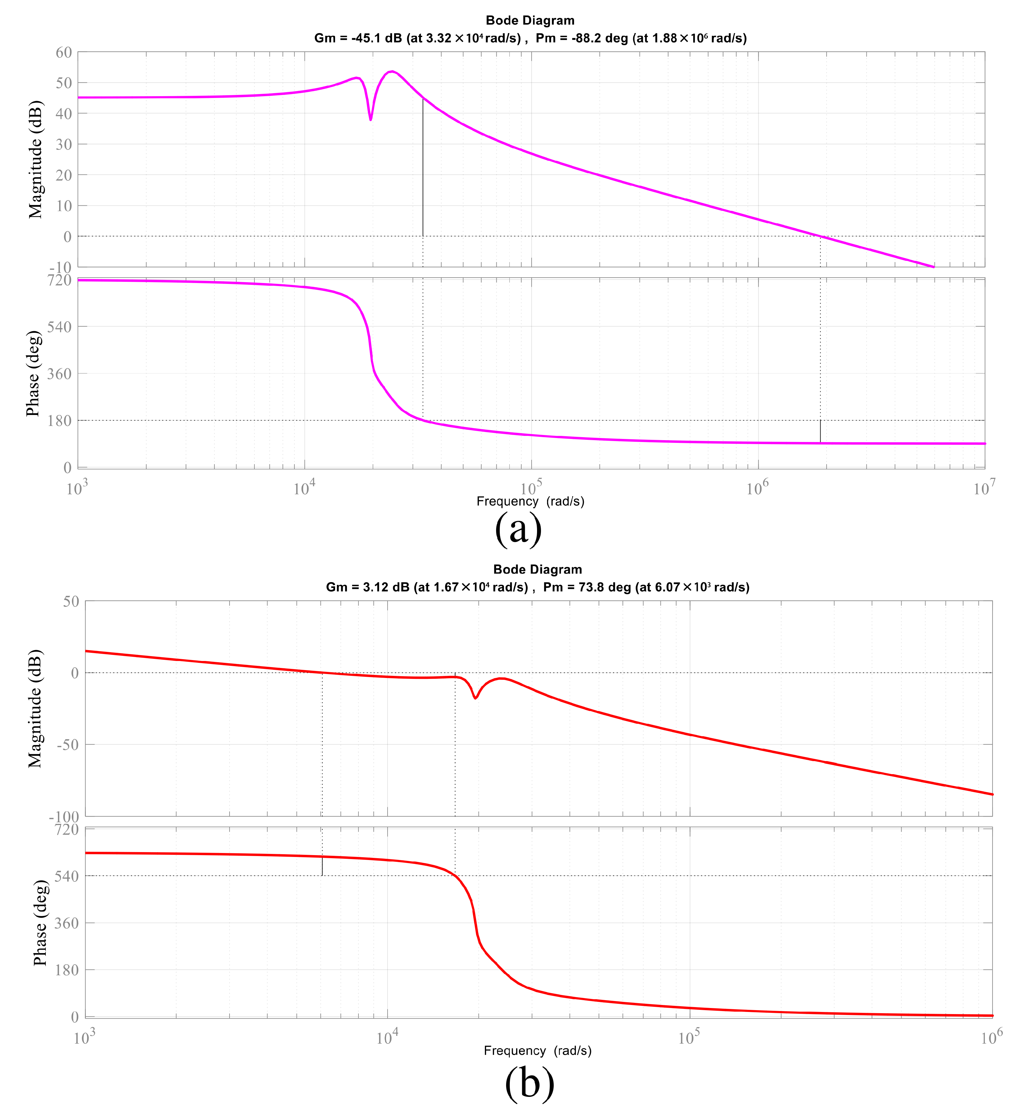
6. Small Signal Analysis

Based on the described relations of the capacitors and the inductors in the second section, the voltage of the inductors and the current of the capacitors can be written as below:
L 1 d i L 1 d t = < v i n > ( 1 d ) < v c 1 > L 2 d i L 2 d t = d < v i n > ( 1 d ) < v c 2 > C 1 d v c 1 d t = ( 1 d ) < i L 1 > < v c 1 + v c 2 R > C 2 d v c 2 d t = ( 1 d ) < i L 2 > < v c 1 + v c 2 R >
All the inductors current, capacitors voltage, and the duty cycle can be expressed as the summation of a DC and an AC term. It is worth noting that the mentioned AC term can be neglected as below:
< i L 1 > = I L 1 + i ^ L 1 , < i L 2 > = I L 2 + i ^ L 2 , < v C 1 > = V C 1 + v ^ C 1 , < v C 2 > = V C 2 + v ^ C 2 , d = D + d ^ i ^ L 1 < < I L 1 , i ^ L 2 < < I L 2 , v ^ C 1 < < V C 1 , v ^ C 2 < < V C 2 , d ^ < < D
The matrices of the space state equations have been expressed as below:
d x ^ d t = A x + B d ^
where
x ^ t = d i ^ L 1 d t , d i ^ L 2 d t , d v ^ C 1 d t , d v ^ C 2 d t ,
A = 0 0 D 1 L 1 0 0 0 0 D 1 L 2 1 D C 1 0 1 R C 1 1 R C 1 0 1 D C 2 1 R C 2 1 R C 2
B t = a 1 , a 2 , a 3 , a 4 C = 0 , 0 , 1 , 1
a 1 = V C 1 L 1 , a 2 = V C 2 L 2 , a 3 = I L 1 C 1 , a 4 = I L 2 C 2
Based on the matrices, the bode diagram of the proposed converter has been extracted and the phase and gain margin have been extracted −45.1 dB and −88.7 deg respectively. The bode diagram has been illustrated in Figure 8a. Based on the expressed space state equations, the compensator of the mentioned system has been calculated as below by MatLab.
C ( S ) = 31.11 s
According to the designed compensator, the bode diagram of the converter after compensating as in Figure 8b.

7. The Comparison of the Different Features of the Proposed Converter and Recently Suggested Topologies in an Operating Point

In Table 1, Table 2, Table 3, Table 4, Table 5 and Table 6, different features have been compared for 90 W output power, the corresponding duty cycle of three times voltage gain, and 1 A output current. It is worth noting that the inductors loss and conduction loss of switches have been compared. It can be understood that the proposed converter has the lowest inductor loss as well as the switch loss in comparison with [15,16,17,18,19,20,21,22,23,24,25,26]. Moreover, the switching loss of the switches, diode loss, corresponding duty cycle, and efficiency have been reported in Table 2. It is worth noting that the switching loss of the proposed converter is more than in [15,16,17,18,19,20,21,22,23,24,25,26]. However, the diode loss of the proposed converter has achieved the lowest value. Moreover, the proposed converter employs a lower value of the duty cycle in comparison with [15,16,17,18,19,20,21,22,23,24,25]. In the third and fourth tables, the normalized values of the voltage/current stresses of semiconductors have been reported and compared. It is worth noting that the output voltage and input current have been considered as the base values of the voltage/current stresses respectively. It can be understood that the voltage stress of the second switch and diode has the lowest value in comparison with [15,16,17,18,19,20,21,22,23,24,25,26]. Moreover, the voltage stress of the first switch and diode has a lower value in comparison with [15,16,17,18,19,20,21,22,23,24,25]. Furthermore, according to Table 3, the current stress of the first switch and diode has the lowest value among [15,16,17,18,19,20,21,22,23,24,25,26]. It is worth noting that the current stress of the second switch in the proposed converter is lower than in [15,16,17,18,19,20,21,22,23,24,25]. It has to be remembered that the current stress of the second diode is the same in all converters. In the fifth table, the number of the circuit components has been compared. It can be understood that the proposed converter has two inductors, capacitors, switches, and diodes, which is the as same as [16,19,20,24,25,26]. In other words, the rest of them have three inductors and capacitors and two switches and diodes. In the sixth table, the stored energy of the inductors has been calculated and reported. It can be understood that the proposed converter has the lowest storage energy. It is worth noting that the dimension of the converter is relative to the stored energy of the converter. Consequently, it can be stated that the proposed converter has the lowest dimension among [15,16,17,18,19,20,21,22,23,24,25,26].

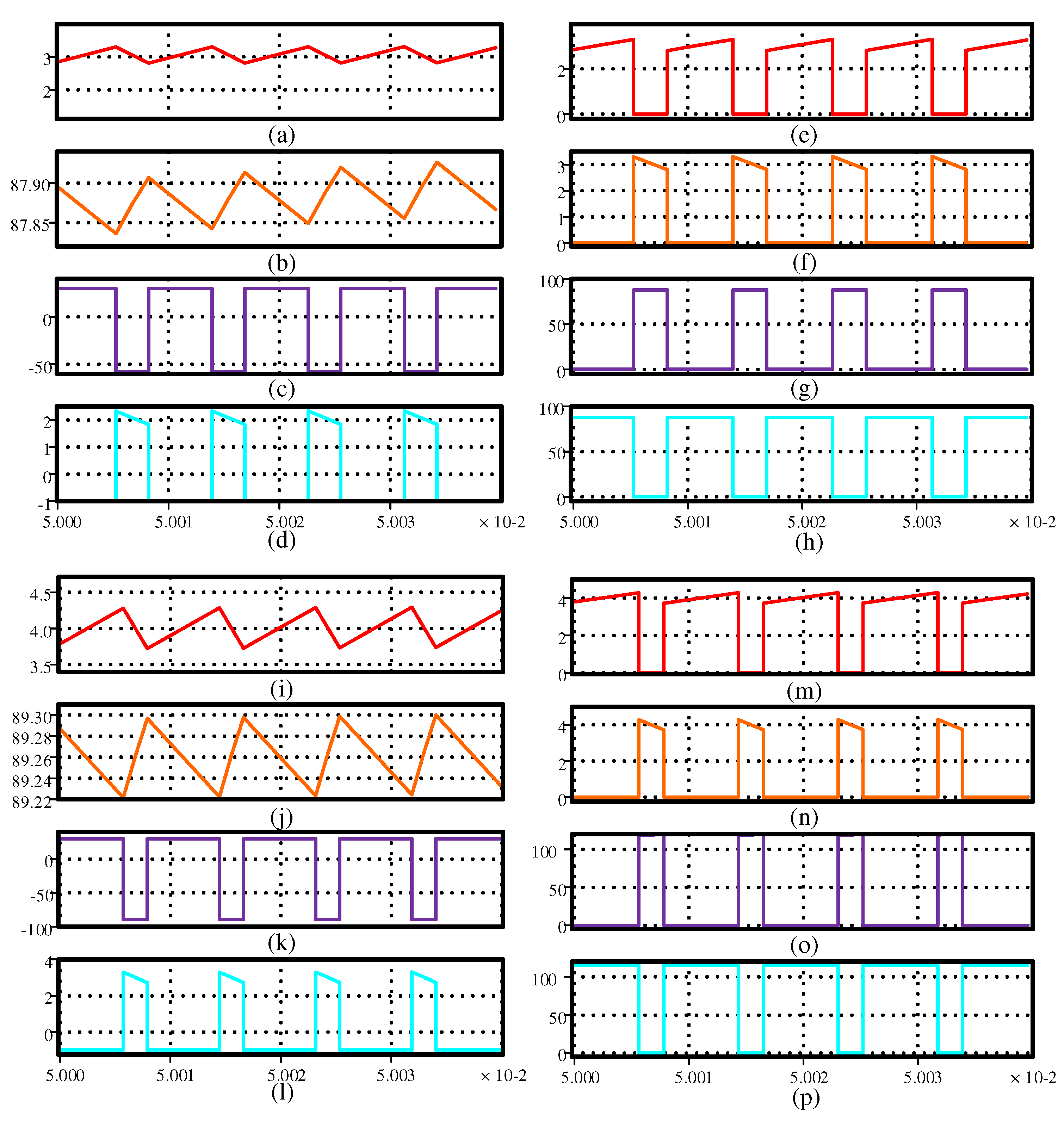
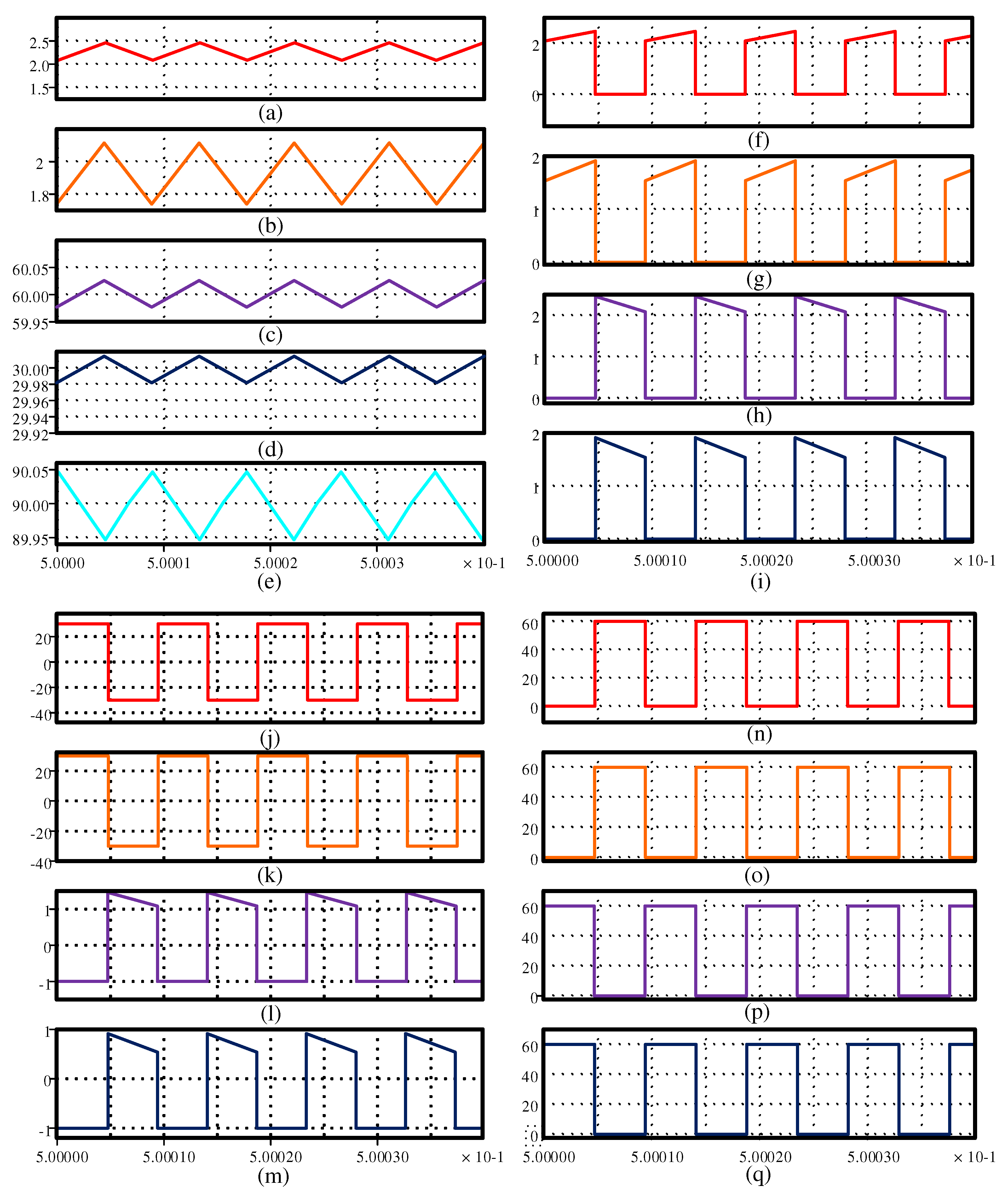
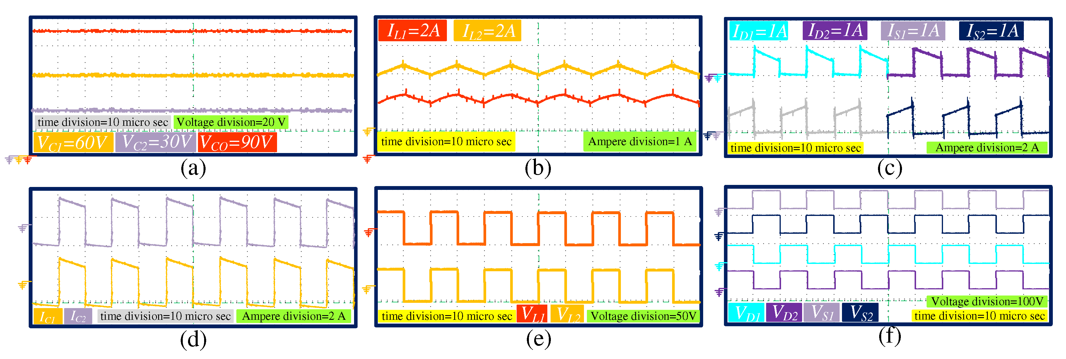
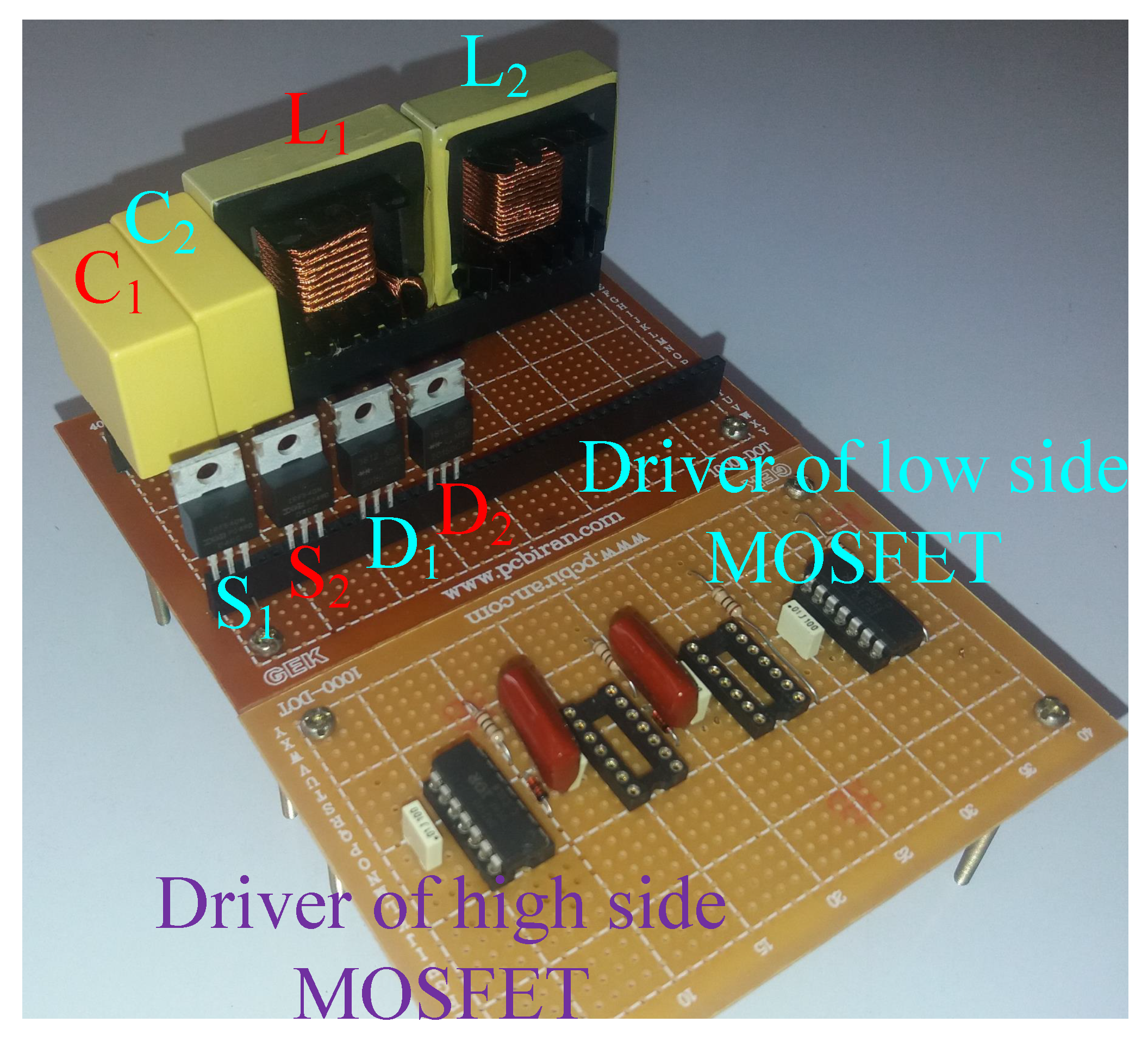
8. Simulation and Experimental Results

To simulate the proposed converter, the inductors’ and capacitors’ values have to be found. Therefore, the expressed equations of current/voltage ripples in (4) are used. In addition, the switching frequency and percentage of current/voltage ripples have to be valued. Due to equipment limits, the frequency has been assumed 100 kHz. Moreover, the current ripple of the inductors and voltage ripple of the capacitors have been considered 30 and 5 percent respectively. It is worth noting that, to use the percentage of the current/voltage ripples with their corresponding equations, the average current of the inductors and average voltage of capacitors have been calculated as (19):
V i n = 30 V , V C 1 = 60 V , V C 2 = 30 V , D = 0.5 I L 1 = I L 2 = 2 A , I o = 1 A
PLECS software has been used to extract the simulation outcomes. The version of the employed software is 4.1.2. The inductors and capacitors value based on (4), (19) are as (20):
L 1 = L 2 > 250 μ H , C 1 > 1.6 μ F , C 2 > 3.2 μ F
The inductors current and capacitors voltage have been presented in Figure 9a–e. The average current of the inductors and average voltage of the capacitors are as (21):
I L 1 = 2 A , I L 2 = 1.8 A , V C 1 = 59.9 V , V C 2 = 30.1 V , V o = 90 V
A comparison between (21) and (19) defines their compatibility. Therefore, the validity of the expressed relations of (2) and (4) is improved. In Figure 9f–i, the current waveforms of the switches and diodes have been illustrated. According to these figures, the average current of the semiconductors is 1 A. Moreover, it can be understood that the switches and diodes operate asynchronously as well as stated in the second section. According to (1), the applied voltage to the inductors is 30 V and −30 V in the first and second modes respectively. It is worth noting that these values are compatible with Figure 9j,k. Moreover, in the first mode, the crossing current from the capacitors is I o . Furthermore, in the second mode I L I o crosses the capacitors. It is worth noting that the current waveforms of Figure 9l,m are compatible with the mentioned concepts. It is also worth noting that the applied voltage to the semiconductors during their inactivation mode is compatible with the extracted equations in (3). In Figure 10, the boost and buck-boost converters have been simulated to increase 30 V input source to 90 V output. It is worth noting that 66 percent and 75 percent duty cycles cause the voltage gain of three in the boost and buck-boost converters respectively. The presented results in Figure 10a–h are for the boost converter and the remaining is for the buck-boost one. In comparison with the proposed converter, the boost and buck-boost converters require a higher duty cycle to have a three times voltage gain. Moreover, according to Figure 10g,h,o,p the semiconductors experience higher voltage during their inactivation mode. Furthermore, based on Figure 10e,f,m,n the semiconductors experience higher current during their activation. Consequently, the proposed converter provides the mentioned voltage gain with a lower duty cycle and semiconductors’ current/voltage stresses. In Figure 11, the details of the used drivers have been presented. Moreover, IRF540 and 2015OCT are the types of MOSFETs and diodes used. Furthermore, all the used capacitors are MKT capacitors with a low equivalent series resistance (ESR). In Figure 12, the experimental results of the proposed converter have been illustrated. Based on the expressed values of the inductors and capacitors in (20), the voltage waveforms of the capacitors and current waveforms of the inductors have been illustrated. In addition, their average values have been expressed in (21):
I L 1 = I L 2 = 2 A , V C 1 = 60 V , V C 2 = 30 V , V o = 90 V
A comparison between the extracted values from experimental and simulation results defines their compatibility. Moreover, according to Figure 12d,e, the current of capacitors and the voltage of the inductors have been presented. Furthermore, their average value is zero and compatible with the current/voltage second balance. It is worth noting that the current/voltage waveforms of the semiconductors have been presented in Figure 12c,d. The average value of their currents is 1 A and compatible with the extracted equation in (3). Furthermore, the applied voltage during inactivation mode is as same as simulation results.
It is worth noting that the voltage gain of the converter has been extracted for different values of the duty cycle from the prototype and compared with the theoretical relation of the non-ideal voltage gain in Figure 13. It can be understood that both results are the same as each other while the duty cycle varies from 67 percent. Moreover, as the duty cycle increases from 67 percent, a difference takes place between the theoretical and experimental results. In Figure 14, the efficiency of the converter has been extracted for the different values of the output powers and 50 percent duty cycle based on the theory and experiment. It is worth noting that the efficiency of the proposed converter varies from 99 to 97.8 percent while the output power varies from 30 W to 180 W. However, based on the experimental results, the efficiency varies from 95.2 to 89 percent in the mentioned interval of the duty cycle. It is good to mention that the differences in the extracted results have occurred due to neglecting some kinds of loss and quality of the used circuit components. This difference is more obvious in Figure 15 where the efficiency has been extracted from the theoretical relations and experimental results for the varying duty cycle from 20 to 80 percent. It is also good to mention that the prototype of the converter has been presented in Figure 16.

9. Conclusions

In this paper, a novel combination of the conventional DC-DC converters was proposed. Due to the use of conventional converters, it was capable of providing a high value of the voltage gain besides a high value of the efficiency. It was discussed that the proposed converter was capable of providing an efficiency higher than 90 for a great interval of the duty cycle. Moreover, the different kinds of losses and current/voltage stresses were expressed and compared with the recently suggested converters in an operating point. Furthermore, the stored energy of the converter was compared with other high gain converters and the lower dimension of the proposed topology was concluded. Additionally, the voltage gain and efficiency of the proposed converter were compared with other high gain converters for all values of the duty cycle. In all the mentioned comparisons the better function of the proposed converter was deduced. It is worth noting that the small-signal analysis was done and a suitable compensator was designed. Finally, the simulation results of the proposed converter were extracted as well as the conventional converters by PLECS and compared with each other. Furthermore, the advantages of the proposed converter were discussed in comparison with the boost and buck-boost converters according to the simulation results. Furthermore, the experimental results were discussed and compared with the simulation results and theoretical considerations. Additionally, the efficiency of the converter was compared based on the theoretical and experimental results, and their differences were discussed for a varying output power besides a constant duty cycle as well as the duty cycle is varying besides a constant output power. It is worth noting that the same study was done for the voltage gain and the extracted equation of the non-ideal voltage gain was validated. It is good to mention that due to the use of buck-boost and boost with each other in the proposed converter, the continuous input current of the proposed converter was provided beside a high current ripple. In future work, the ZVS and ZCS techniques are going to be investigated in the proposed topology, and a strong control method to be applied to its controlling concepts. As the last concept, this converter is not suitable for high power applications and it is recommended to employ this topology for output powers that are lower than 200 W.

Author Contributions

Conceptualization, T.R., M.R.I., H.G., S.M. and E.A.; methodology, T.R., M.R.I., H.G., S.M. and E.A.; software, T.R., M.R.I., H.G., S.M. and E.A.; validation, T.R., M.R.I., H.G., S.M. and E.A.; formal analysis, T.R., M.R.I., H.G., S.M. and E.A.; resources, T.R., M.R.I., H.G., S.M. and E.A.; writing—original-draft preparation, T.R., M.R.I., H.G., S.M. and E.A.; writing—review and editing, T.R., M.R.I., H.G., S.M. and E.A.; supervision, T.R., M.R.I. and E.A.; project administration, T.R., M.R.I., H.G., S.M. and E.A. All authors have read and agreed to the published wersion of the manuscript.

Funding

This work is supported by the China Postdoctoral Science Foundation through grants: (2019M662357).

Data Availability Statement

Data available on request from the authors.

Conflicts of Interest

The authors declare no conflict of interest.

References

  1. Gopi, R.R.; Sreejith, S. Converter topologies in photovoltaic applications—A review. Renew. Sustain. Energy Rev. 2018, 94, 1–14. [Google Scholar] [CrossRef]
  2. Amir, A.; Amir, A.; Che, H.S.; Elkhateb, A.; Abd Rahim, N. Comparative analysis of high voltage gain DC-DC converter topologies for photovoltaic systems. Renew. Energy 2019, 136, 1147–1163. [Google Scholar] [CrossRef] [Green Version]
  3. Revathi, B.S.; Prabhakar, M. Non isolated high gain DC-DC converter topologies for PV applications—A comprehensive review. Renew. Sustain. Energy Rev. 2016, 66, 920–933. [Google Scholar] [CrossRef]
  4. Taghvaee, M.; Radzi, M.; Moosavain, S.; Hizam, H.; Marhaban, M.H. A current and future study on non-isolated DC–DC converters for photovoltaic applications. Renew. Sustain. Energy Rev. 2013, 17, 216–227. [Google Scholar] [CrossRef]
  5. Marjani, J.; Imani, A.; Hekmati, A.; Afjei, E. A new dual output DC-DC converter based on SEPIC and Cuk converters. In Proceedings of the 2016 International Symposium on Power Electronics, Electrical Drives, Automation and Motion (SPEEDAM), Capri, Italy, 1 August 2016; pp. 946–950. [Google Scholar]
  6. Gholizadeh, H.; Sharifi Shahrivar, R.; Hashemi, M.R.; Afjei, E.; A Gorji, S. Design and Implementation a Single-Switch Step-Up DC-DC Converter Based on Cascaded Boost and Luo Converters. Energies 2021, 14, 3584. [Google Scholar] [CrossRef]
  7. Tewari, N.; Sreedevi, V. A novel single switch DC-DC converter with high voltage gain capability for solar PV based power generation systems. Sol. Energy 2018, 171, 466–477. [Google Scholar] [CrossRef]
  8. Ghaderi, D.; Maroti, P.K.; Sanjeevikumar, P.; Holm-Nielsen, J.B.; Hossain, E.; Nayyar, A. A Modified Step-Up Converter with Small Signal Analysis-Based Controller for Renewable Resource Applications. Appl. Sci. 2020, 10, 102. [Google Scholar] [CrossRef] [Green Version]
  9. Almalaq, Y.; Matin, M. Three Topologies of a Non-Isolated High Gain Switched-Inductor Switched-Capacitor Step-Up Cuk Converter for Renewable Energy Applications. Electronics 2018, 7, 94. [Google Scholar] [CrossRef] [Green Version]
  10. Wu, Y.-E.; Hsiao, S.-L. Novel High-Efficiency Three-Port Bidirectional Step-Up/Step-Down DC–DC Converter for Photovoltaic Systems. Sustainability 2021, 13, 7913. [Google Scholar] [CrossRef]
  11. Meraj, M.; Bhaskar, M.S.; Reddy, B.P.; Iqbal, A. Non-Isolated DC–DC Power Converter With High Gain and Inverting Capability. IEEE Access 2021, 9, 62084–62092. [Google Scholar] [CrossRef]
  12. Abbasi, M.; Abbasi, E.; Li, L.; Tousi, B. Design and Analysis of a High-Gain Step-Up/Down Modular DC–DC Converter with Continuous Input Current and Decreased Voltage Stress on Power Switches and Switched-Capacitors. Sustainability 2021, 13, 5243. [Google Scholar] [CrossRef]
  13. Rajaei, A.; Shahparasti, M.; Nabinejad, A.; Savaghebi, M. A High Step-Up Partial Power Processing DC/DC T-Source Converter for UPS Application. Sustainability 2020, 12, 10464. [Google Scholar] [CrossRef]
  14. Forouzesh, M.; Siwakoti, Y.P.; Gorji, S.A.; Blaabjerg, F.; Lehman, B. Step-Up DC–DC Converters: A Comprehensive Review of Voltage-Boosting Techniques, Topologies, and Applications. IEEE Trans. Power Electron. 2017, 32, 9143–9178. [Google Scholar] [CrossRef]
  15. Gholizadeh, H.; Salehi, M.; Rafiee, Z.; Afjei, E.; Hamzeh, M. A Transformer less Quadratic Buck-Boost Converter with Wide Range of Output Voltage and Low Switch Stresses. In Proceedings of the 2020 11th Power Electronics, Drive Systems, and Technologies Conference (PEDSTC), Tehran, Iran, 4–6 February 2020; pp. 1–6. [Google Scholar]
  16. Miao, S.; Wang, F.; Ma, X. A New Transformerless Buck-Boost Converter With Positive Output Voltage. IEEE Trans. Ind. Electron. 2016, 63, 2965–2975. [Google Scholar] [CrossRef]
  17. Sarikhani, A.; Allahverdinejad, B.; Hamzeh, M.; Afjei, E. A continuous input and output current quadratic buck-boost converter with positive output voltage for photovoltaic applications. Sol. Energy 2019, 188, 19–27. [Google Scholar] [CrossRef]
  18. Gholizadeh, H.; Sarikhani, A.; Hamzeh, M. A Transformerless Quadratic Buck-Boost Converter Suitable for Renewable Applications. In Proceedings of the 2019 10th International Power Electronics, Drive Systems and Technologies Conference (PEDSTC), Shiraz, Iran, 25 April 2019; pp. 470–474. [Google Scholar]
  19. Babazadeh, Y.; Babaei, E.; Sabahi, M. A New Non-Isolated Buck-Boost Converter with High Voltage Gain and Positive Output Voltage for Renewable Energy Applications. In Proceedings of the 2019 10th International Power Electronics, Drive Systems and Technologies Conference (PEDSTC), Shiraz, Iran, 25 April 2019; pp. 201–206. [Google Scholar]
  20. Rosas-Caro, J.C.; Valdez-Resendiz, J.E.; Mayo-Maldonado, J.C.; Alejo-Reyes, A.; Valderrabano-Gonzalez, A. Quadratic buck–boost converter with positive output voltage and minimum ripple point design. IET Power Electron. 2018, 11, 1306–1313. [Google Scholar] [CrossRef]
  21. Rosas-Caro, J.C.; Sanchez, V.M.; Valdez-Resendiz, J.E.; Mayo-Maldonado, J.C.; Beltran-Carbajal, F.; Valderrabano-Gonzalez, A. Quadratic buck-boost converter with positive output-voltage and continuous input-current. In Proceedings of the 2018 International Conference on Electronics, Communications and Computers (CONIELECOMP), Cholula, Mexico, 21–23 February 2018; pp. 152–158. [Google Scholar]
  22. Totonchi, N.; Gholizadeh, H.; Afjei, E.; Hamzeh, M. A Novel Transformer less High Gain DC-DC Converter with Continuous Input Current and Suitable for Photo Voltaic Panels. In Proceedings of the 2020 11th Power Electronics, Drive Systems, and Technologies Conference (PEDSTC), Tehran, Iran, 4–6 February 2020; pp. 1–6. [Google Scholar]
  23. Gholizadeh, H.; Aboufazeli, S.; Rafiee, Z.; Afjei, E.; Hamzeh, M. A Non-Isolated High Gain DC-DC Converters with Positive Output Voltage and Reduced Current Stresses. In Proceedings of the 2020 11th Power Electronics, Drive Systems, and Technologies Conference (PEDSTC), Tehran, Iran, 4–6 February 2020; pp. 1–6. [Google Scholar]
  24. Garcia-Vite, P.M.; Soriano-Rangel, C.A.; Rosas-Caro, J.C.; Mancilla-David, F. A DC-DC converter with quadratic gain and input current ripple cancelation at a selectable duty cycle. Renew. Energy 2017, 101, 431–436. [Google Scholar] [CrossRef]
  25. Garcia-Vite, P.M.; Valdez-Resendiz, J.E.; Mayo-Maldonado, J.C.; Rosas-Caro, J.C.; Rosario Rivera-Espinosa, M.; Valderrabano-Gonzalez, A. Quadratic gain converter with output voltage ripple mitigation. In Proceedings of the 2017 IEEE Energy Conversion Congress and Exposition (ECCE), Cincinnati, OH, USA, 1–5 October 2017; pp. 2253–2259. [Google Scholar]
  26. Ding, S.; Wang, F. A New Negative Output Buck–Boost Converter with Wide Conversion Ratio. IEEE Trans. Ind. Electron. 2017, 64, 9322–9333. [Google Scholar] [CrossRef]
Figure 1. (a) The comparison of the ideal/non-ideal voltage gains of buck-boost and boost converters, (b) the non-ideal voltage gain of the boost converter for the different output powers, (c) the non-ideal voltage gain of the buck-boost converter for the different output powers, (d) the efficiency of the conventional converters.
Sustainability 13 10699 g001
Figure 2. (a) The proposed topology, (b) the procedure of its creation, (c) the equivalent circuit of the first mode, (d) the equivalent circuit of the second mode.
Sustainability 13 10699 g002
Figure 3. The operation region of the converter in CCM or DCM while: (a) the output voltage is constant, (b) the input voltage is constant.
Sustainability 13 10699 g003
Figure 4. (a) The comparison of the ideal/non-ideal voltage gain of the proposed converter, (b) the non-ideal voltage gain of the proposed converter for the different output powers, (c) the behavior of the voltage gain while the duty cycle and output power are varying, (d) the comparison of the non-ideal voltage gain of the proposed converter and suggested converters of [15,16,17,18,19,20,21,22,23,24,25,26].
Sustainability 13 10699 g004
Figure 5. (a) The efficiency of the proposed converter for the different output powers while the duty cycle varies from 0 to 50, (b) the efficiency of the proposed converter for the different output powers while the duty cycle varies from 50 to 100, (c) the efficiency of the proposed converter while the duty cycle and output powers are varying, (d) the comparison of the efficiency among the proposed converter and converters of [15,16,17,18,19,20,21,22,23,24,25,26] while the duty cycle varies from 0 to 50 percent, (e) the comparison of the efficiency among the proposed converter and converters of [15,16,17,18,19,20,21,22,23,24,25,26] while the duty cycle varies from 50 to 100 percent.
Sustainability 13 10699 g005
Figure 6. (a) The comparison of the inductor loss among the proposed converter and the suggested converters of [15,16,17,18,19,20,21,22,23,24,25,26] while the duty cycle varies from 0 to 50 percent, (b) the comparison of the inductor loss among the proposed converter and the suggested converters of [15,16,17,18,19,20,21,22,23,24,25,26] while the duty cycle varies from 50 to 100 percent, (c) the comparison of the switch loss among the proposed converter and the suggested converters of [15,16,17,18,19,20,21,22,23,24,25,26] while the duty cycle varies from 0 to 50 percent, (d) the comparison of the switch loss among the proposed converter and the suggested converters of [15,16,17,18,19,20,21,22,23,24,25,26] while the duty cycle varies from 50 to 100 percent, (e) the comparison of the diode loss among the proposed converter and the suggested converters of [15,16,17,18,19,20,21,22,23,24,25,26] while the duty cycle varies from 0 to 100 percent.
Sustainability 13 10699 g006
Figure 7. The percentage of the efficiency and losses while: (a) the output power is 30 W, (b) the output power is 60 W, (c) the output power is 90 W, (d) the output power is 120 W, (e) the output power is 150 W, (f) the output power is 180 W.
Sustainability 13 10699 g007
Figure 8. The bode diagram: (a) before compensating, (b) after compensating.
Sustainability 13 10699 g008
Figure 9. The simulation results of the proposed converter: (a) the first inductor current, (b) the second inductor current, (c) the first capacitor voltage, (d) the second capacitor voltage, (e) the output capacitor voltage, (f) the first switch current, (g) the second switch current, (h) the first diode current, (i) the second diode current, (j) the first inductor voltage, (k) the second inductor voltage, (l) the first capacitor current, (m) the second capacitor current, (n) the first switch voltage, (o) the second switch voltage, (p) the first diode voltage, (q) the second diode voltage.
Sustainability 13 10699 g009
Figure 10. The simulation results of the boost converter: (a) the first inductor current, (b) the output voltage, (c) the inductor’s voltage, (d) the capacitor’s current, (e) the switch current, (f) the diode current, (g) the switch voltage, (h) the diode voltage, and the simulation results of the buck-boost converter (i) the first inductor current, (j) the output voltage, (k) the inductor voltage, (l) the capacitor’s current, (m) the switch current, (n) the diode current, (o) the switch voltage, (p) the diode voltage.
Sustainability 13 10699 g010
Figure 11. How to use the IRF2110 MOSFET driver.
Sustainability 13 10699 g011
Figure 12. Experimental results: (a) the capacitor’s voltage, (b) the inductor’s current, (c) the semiconductor’s current, (d) the capacitor’s current, (e) the inductor’s voltage, (f) the semiconductor’s voltage.
Sustainability 13 10699 g012
Figure 13. The comparison of the non-ideal voltage gain based on theory and practical voltage gain based on the experiment.
Sustainability 13 10699 g013
Figure 14. The comparison of the theoretical and experimental efficiency for different output powers, 90 V output voltage, and 50 percent duty cycle.
Sustainability 13 10699 g014
Figure 15. The comparison of the theoretical and experimental efficiency for 90 W output power while: (a) the duty cycle varies from 20 to 50 percent, (b) the duty cycle varies from 50 to 80 percent.
Sustainability 13 10699 g015
Figure 16. The prototype.
Sustainability 13 10699 g016
Table 1. Comparison of power loss.
Inductors LossSwitches Conduction Loss
proposed converters P o r L R 2 ( 1 D ) 2 = 0.36 P o r S R 2 D ( 1 D ) 2 = 0.18
[15] P o r L R D 4 2 D 3 + 3 D 2 2 D + 1 ( 1 D ) 4 = 1.26 P o r S R 2 D 3 2 D 2 + D ( 1 D ) 4 = 0.7
[16] P o r L R 2 D 4 6 D 3 + 8 D 2 4 D + 1 ( 1 D ) 4 = 0.43 P o r S R 2 D 3 2 D 2 + D ( 1 D ) 4 = 0.7
[17] P o r L R 3 D 4 5 D 3 + 7 D 2 4 D + 1 ( 1 D ) 4 = 1 P o r S R 5 D 3 4 D 2 + D ( 1 D ) 4 = 0.6
[18] P o r L R 2 D 4 6 D 3 + 8 D 2 4 D + 1 ( 1 D ) 4 = 1 P o r S R 2 D 3 2 D 2 + D ( 1 D ) 4 = 0.7
[19] P o r L R 2 D 2 2 D + 1 ( 1 D ) 4 = 1.14 P o r S R 2 D 3 2 D 2 + D ( 1 D ) 4 = 0.7
[20] P o r L R 2 D 2 2 D + 1 ( 1 D ) 4 = 1.14 P o r S R 2 D 3 2 D 2 + D ( 1 D ) 4 = 0.7
[21] P o r L R 5 D 2 6 D + 2 ( 1 D ) 4 = 0.43 P o r S R 5 D 3 6 D 2 + 2 D ( 1 D ) 4 = 0.27
[22] P o r L R 3 D 2 4 D + 2 ( 1 D ) 4 = 0.91 P o r S R 2 D 3 6 D 2 + 5 D ( 1 D ) 4 = 1.67
[23] P o r L R 2 D 4 6 D 3 + 8 D 2 4 D + 1 ( 1 D ) 4 = 0.55 P o r S R 2 D 3 2 D 2 + D ( 1 D ) 4 = 0.4
[24] P o r L R D 2 2 D + 2 ( 1 D ) 4 = 1.6 P o r S R D 3 2 D 2 + 2 D ( 1 D ) 4 = 0.9
[25] P o r L R 2 D 2 2 D + 1 ( 1 D ) 4 = 0.67 P o r S R 2 D 3 2 D 2 + 2 D ( 1 D ) 4 = 0.4
[26] P o r L R 2 D 2 2 D + 1 ( 1 D ) 4 = 0.36 P o r S R D 3 2 D 2 + D ( 1 D ) 4 = 0.45
Table 2. Comparison of power loss.
Switching Loss of SwitchesDiodes LossDuty Cycle
proposed converters f s P o t o f f D 1 D 2 = 0.06 2 V D F I o = 1 0.5
[15] f s P o t o f f ( 1 + D ) 1 D = 0.04 V D F I o 1 D = 1.315 0.62
[16] f s P o t o f f 1 D = 0.02 V D F I o 1 D = 1.31 0.62
[17] f s P o t o f f D ( 1 D ) 2 = 0.04 V D F I o 1 D = 1.31 0.62
[18] f s P o t o f f 1 D = 0.02 V D F I o 1 D = 1.31 0.62
[19] f s P o t o f f 1 D = 0.02 V D F I o 1 D = 1.31 0.62
[20] f s P o t o f f 1 D = 0.02 V D F I o 1 D = 1.31 0.62
[21] f s P o t o f f ( 3 D 1 ) D ( 1 D ) = 0.11 V D F I o 1 D = 1.31 0.62
[22] f s P o t o f f ( 1 + D ) 1 D = 0.03 V D F I o ( 1 + D ) 1 D = 1.8 0.57
[23] f s P o t o f f ( 1 + D ) 1 D = 0.03 V D F I o 1 D = 1.15 0.57
[24] f s P o t o f f ( 1 + D ) 1 D = 0.03 V D F I o ( 2 D ) 1 D = 1.65 0.57
[25] f s P o t o f f ( 1 + D ) 1 D = 0.03 V D F I o 1 D = 1.15 0.57
[26] f s P o t o f f ( 1 D ) ( 2 D ) = 0.01 V D F I o ( 1 + D ) 1 D = 1.5 0.5
Table 3. Comparison of voltage stress.
V S 1 V O V S 2 V O V D 1 V O V D 2 V O
proposed converter 1 1 + D = 0.67 1 1 + D = 0.67 1 1 + D = 0.67 1 1 + D = 0.67
[15] 1 D D 2 = 11 1 D D 2 = 1 1 D = 1.61
[16] 1 D D 2 = 1 1 D = 1.61 1 D D 2 = 1 1 D = 1.61
[17] 1 D 2 = 2.68 1 D = 1.61 1 D D 2 = 1 1 D = 1.61
[18] 1 D D 2 = 1 1 D = 1.61 1 D D 2 = 1 1 D = 1.61
[19] 1 D D 2 = 1 1 D = 1.61 1 D D 2 = 1 1 D = 1.61
[20] 1 D D 2 = 1 1 D = 1.61 1 D D 2 = 1 1 D = 1.61
[21] 1 D D 2 = 1 1 D = 1.61 1 D D 2 = 1 1 D = 1.61
[22] 1 D D 2 = 1.32 2 D 1 D = 1.61 1 D D = 0.751
[23] 1 D D = 0.75 1 D = 1.61 1 D D = 0.75 1 D = 1.75
[24] 1 D D = 0.751 1 D D = 0.751
[25] 1 D D = 0.75 1 D = 1.75 1 D D = 0.75 1 D = 1.75
[26] 1 D D ( 2 D ) = 0.67 1 D ( 2 D ) = 1.33 1 D D ( 2 D ) = 0.67 1 D ( 2 D ) = 1.33
Table 4. Comparison of current stresses.
I S 1 I i n I S 2 I i n I D 1 I i n I D 2 I i n D
proposed converter D 1 + D = 0.34 D 1 + D = 0.34 1 D 1 + D = 0.34 1 D 1 + D = 0.34 0.5
[15]1 1 D D = 0.61 1 D D = 0.61 1 D D 2 = 0.340.62
[16]1 1 D D = 0.61 1 D D = 0.61 1 D D 2 = 0.340.62
[17]1 2 D 1 D = 0.61 2 D 1 D = 0.61 1 D D 2 = 0.340.62
[18]1 1 D D = 0.61 1 D D = 0.61 1 D D 2 = 0.340.62
[19]1 1 D D = 0.61 1 D D = 0.61 1 D D 2 = 0.340.62
[20]1 1 D D = 0.61 1 D D = 0.61 1 D D 2 = 0.340.62
[21]1 1 D D = 0.61 1 D D = 0.61 1 D D 2 = 0.340.62
[22] 2 D = 1.43 1 D = 0.43 1 D D = 0.75 ( 1 D ) 2 D = 0.340.57
[23]D = 0.57 1 D = 0.43 1 D = 0.43 ( 1 D ) 2 D = 0.340.57
[24]1 1 D = 0.43 1 D D = 0.75 ( 1 D ) 2 D = 0.340.57
[25]D = 0.57 1 D = 0.43 1 D = 0.43 ( 1 D ) 2 D = 0.340.57
[26] 1 D ( 2 D ) = 1.34 1 D 2 D = 0.34 1 D D ( 2 D ) = 0.67 ( 1 D ) 2 D ( 2 D ) = 0.340.5
Table 5. Comparison of components number and voltage gain.
No. LNo. CNo. SNo. DNo.
[15]332210
[16]22228
[17]332210
[18]332210
[19]22228
[20]22228
[21]22228
[22]332210
[23]332210
[24]22228
[25]22228
[26]22228
proposed22228
Table 6. Comparison of stored energy.
Stored Energy of Inductors
proposed converters 2 D 1 + D V 2 o 2 k f s R = 1 mJ
[15] 1 + D D V 2 o 2 k f s R = 3.91 mJ
[16] 2 V 2 o 2 k f s R = 3 mJ
[17] 2 V 2 o 2 k f s R = 3 mJ
[18] 2 V 2 o 2 k f s R = 3 mJ
[19] 2 V 2 o 2 k f s R = 3 mJ
[20] 2 V 2 o 2 k f s R = 3 mJ
[21] 2 V 2 o 2 k f s R = 3 mJ
[22] ( 1 + D ) V 2 o 2 k f s R = 2.35 mJ
[23] ( 1 + D ) V 2 o 2 k f s R = 2.35 mJ
[24] ( 1 + D ) V 2 o 2 k f s R = 2.35 mJ
[25] ( 1 + D ) V 2 o 2 k f s R = 2.35 mJ
[26] 2 2 D V 2 o 2 k f s R = 2 mJ
Publisher’s Note: MDPI stays neutral with regard to jurisdictional claims in published maps and institutional affiliations.

