Article

Operation of a UXE-Type 11-Level Inverter with Voltage-Balance Modulation Using NLC and ACO-Based SHE

1
Department of Electrical Engineering, Z.H. College of Engineering & Technology, Aligarh Muslim University, Aligarh 202001, India
2
Department of Electrical Engineering, National Taiwan University of Science and Technology, Taipei City 10607, Taiwan
3
Capability Systems Centre, School of Engineering and IT, UNSW Canberra at ADFA, Canberra, ACT 2612, Australia
4
Department of Electrical Engineering, College of Engineering, Taif University, Taif 21944, Saudi Arabia
*
Authors to whom correspondence should be addressed.
Sustainability 2021, 13(16), 9035; https://doi.org/10.3390/su13169035
Submission received: 29 June 2021 / Revised: 2 August 2021 / Accepted: 4 August 2021 / Published: 12 August 2021
(This article belongs to the Special Issue Renewable Energy: Technologies and Challenges)

Abstract

:
In this article, the UXE-Type inverter is considered for eleven-level operation. This topology exhibits a boosting capability along with reduced switches and one source. An algorithm that utilizes the redundant states to control the voltage-balance of the auxiliary direct current (DC)-link is presented. The proposed control algorithm is capable of maintaining the voltages of each capacitor at V d c / 4 resulting in a successful multilevel operation for all values of load. The inverter is also compared with 11-level inverters. The modulation of the inverter is performed by employing nearest level control and ant colony optimization based selective harmonic elimination. The maximum inverter efficiency is 98.1% and its performance is validated on an hardware-in-the-loop platform.

1. Introduction

Multilevel inverter (MLI) and its types are becoming popular in the research and industrial communities for industry applications. They are being considered for integration of renewable energy source [1] and drives [2] due to near to sine waveform generation, and exhibition of lower switch stresses. The increase in the number of levels in the output voltage leads to an increase in the number of capacitors in the conventional Flying Capacitor (FC) inverters, a larger number of clamping diodes in the Neutral Point Clamped (NPC) inverters, and an increment in the DC sources in the Cascaded H-Bridge (CHB) based structures [3,4,5]. Thus, new MLI structures with reduced component count are being considered [6].
Single-phase MLIs are divided into symmetrical (SMLI) and asymmetrical (AMLI) categories on the basis values of the sources used. The former category uses the DC sources of the same values and the latter of different value. The examples of symmetrical MLI are the NPC, and FC [7,8]. As discussed earlier, these structures require a large number of components. For example, a seven-level NPC requires 6 capacitors, 12 switches, and 10 diodes; a seven-level FC requires 6 capacitors and 12 switches; the CHB requires 3 DC sources and 12 switches. The AMLIs employ sources of different magnitudes and leads to the reduction of components. For example, the packed U-cell AMLI requires a 2 capacitors and 6 switches to generate a 7-level output [9]. This further results in better efficiency of the inversion process [6].
In MLIs with switched capacitor structures (SCMLI), the capacitor voltages and the DC-sources are employed to obtain a particular voltage level and simultaneous charging and discharging of the capacitors. SCMLI can be an SMLI or AMLI and require a fewer number of switches than the conventional MLIs. Besides, these topologies exhibit the features of boosting, and small filter components [10,11]. In recent years, a myriad of SCMLIs have been presented in the literature. Siddiqui et al. in [12] propose a 7-level SCMLI that employs a single source, 10 IGBTs, four diodes and two capacitors. Roy in [13] presents an SCMLI with a criss-cross switch structure. In [14], a SCMLI with a 9-level output is presented and Siddiqui et al. in [15] presents an SCMLI with 11-level output and a cascaded operation [15].
New MLI topologies utilize the advantages of the FC MLI and the CHB MLI. The first hybridization resulted in the five/seven-level Packed U-Cell (PUC) inverter [9]. A modified PUC (MPUC) was presented by Vahedi et al. in [10], where a ratio of 2:1 between the DC links produces 7-level output. Forty-nine and 25-level operation was discussed in [16,17] respectively, by cascading the MPUC. The modified version of PUC was the Packed E-cell (PEC) inverter [18] where the DC-link was divided into two voltage partitions forming a 9-level inverter. Recently, a 13-level inverter was introduced by Kim et al. in [19] that employed single source, three capacitors and 14 IGBTs. 11-level structures are few but are discussed in the literature. Sotoodeh et al. in [20] utilized half-bridge units to develop an 11-level modular MLI for FACTS systems, and an 11-level cascaded H-bridge structure is explored for induction-furnace application [21]. Authors in [22,23] apply an asymmetrical hybrid CHB structure for 3-phase application. The latest 11-level topologies in literature are compared and discussed later in the paper.
This work presents a new UXE-type inverter that can produce 11-levels in its output voltage. It uses one DC-source, 12 IGBTs and two capacitors. Two of these switches form an AC switch. Also, the converter requires only one voltage sensor to sense DC-link voltage despite employing two capacitors. This inverter and voltage balance control has been filed and published as provisional Patent in the Indian Patent Office with application number: 202011029808 A. The presented topology finds its basis in the topologies presented in [9,18], as shown in Figure 1. It is also found that the cost factor of the presented structure is less than the other 11-level inverters due to the use of a reduced number of gate drivers.
Inverters are modulated with high-frequency or low-frequency switching techniques, depending on frequency of level shifts in a cycle of operation. Sine-PWM [24] and its extensions [11,18], space vector PWM (SVPWM) [7] belong to the high-switching frequency category. Selective harmonic elimination (SHE) [25], selective harmonic mitigation (SHM) [26] and Nearest level control (NLC) [15,27] belong to a low-switching frequency category. In SHE and SHM, the angles are decided either by analytical tools like Newton-Rapson method [28] or by nature-inspired techniques like genetic algorithm (GA) [29], grey wolf optimization [23], differential evolution (DE) [30], projectile target search algorithm [31], or particle swarm optimization (PSO) [25], where the transcendental equations are solved under constrained environment.
The operation of the presented inverter is considered under two low switching frequency schemes: (a) A modified NLC (MNLC) scheme, where both the zero states of the converter are utilized will be developed and implemented; and (b) Ant colony optimization (ACO)-based SHE scheme to remove the low-order odd-harmonics from the voltage. The NLC leads to a reduction of low-order harmonics, and this technique benefits closed-loop operation [15]. On the other hand, the SHE leads to the selected low-order harmonics’ elimination due to the direct control on the harmonic spectrum [28]. The ACO algorithm is utilized to generate the optimum angles of operation over a wide range of modulation indexes by solving the transcendental equations. This technique utilizes the distinctive feature of ant’s food searching through shortest route [32], and has been utilized to solve the SHE equations for 3-level active neutral point clamped inverter in [33].
The paper is organized as follows. Firstly, the analysis of the circuit and switching states of the UXE-11 are discussed. In Section 3, a comparison of the UXE-11 inverter with eleven level inverters is presented. In Section 4 and Section 5 the modified NLC and the ACO-based SHE algorithms are discussed for the inverter’s modulation. In addition, these sections also discuss the balancing of the capacitor bank employing redundant states in detail. In Section 6, power loss analysis is carried out in the PLECS environment. Finally, the paper is concluded with the result validation in hardware in the loop environment.

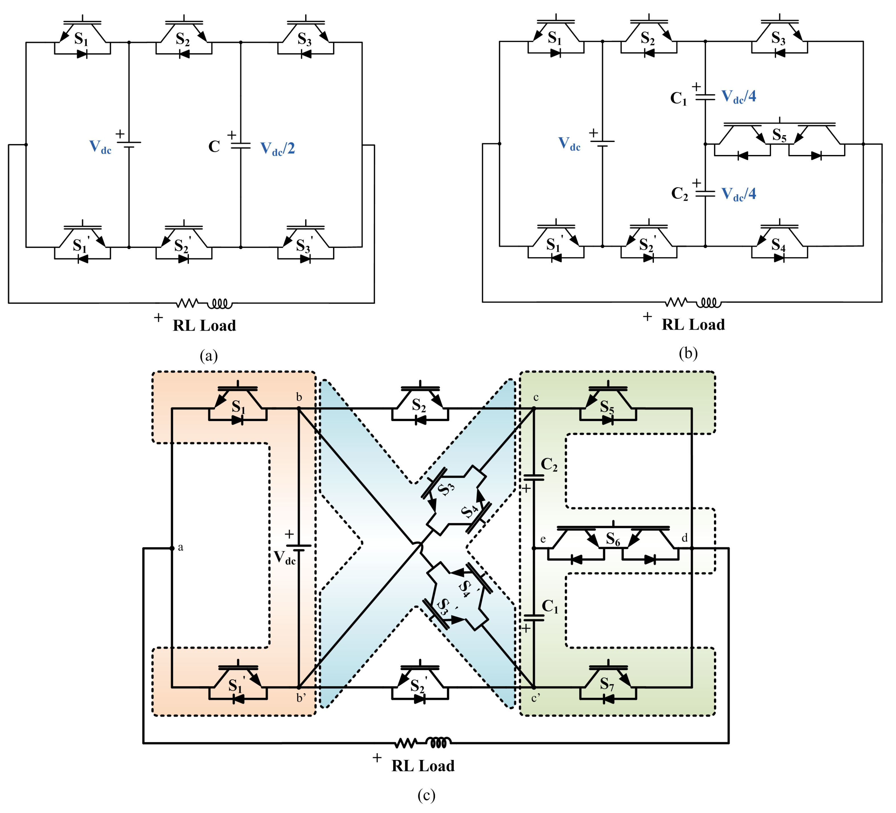
2. The UXE-Type Inverter

2.1. UXE-Type Inverter Circuit
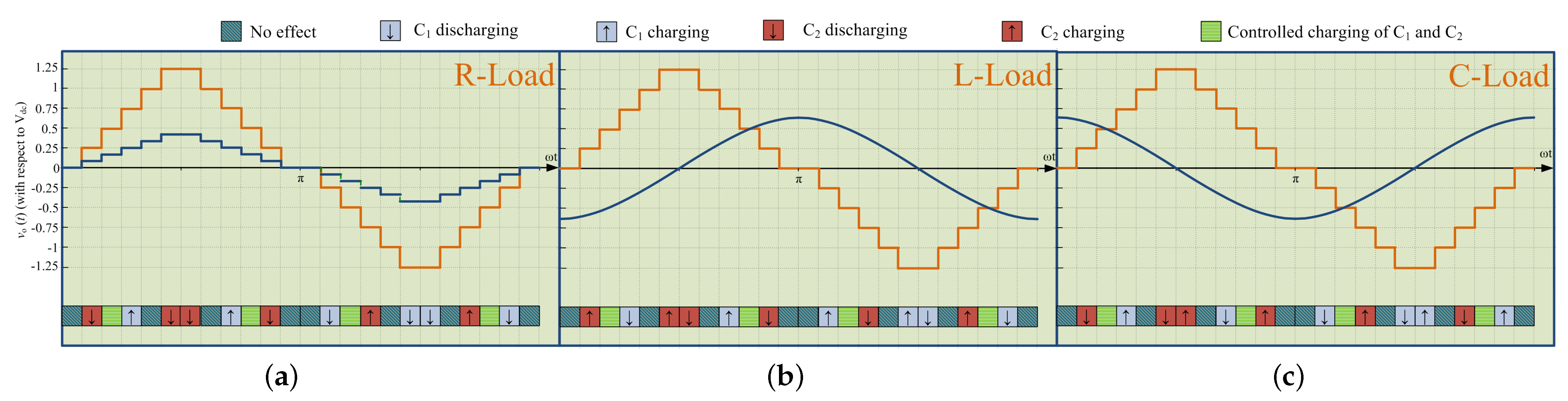
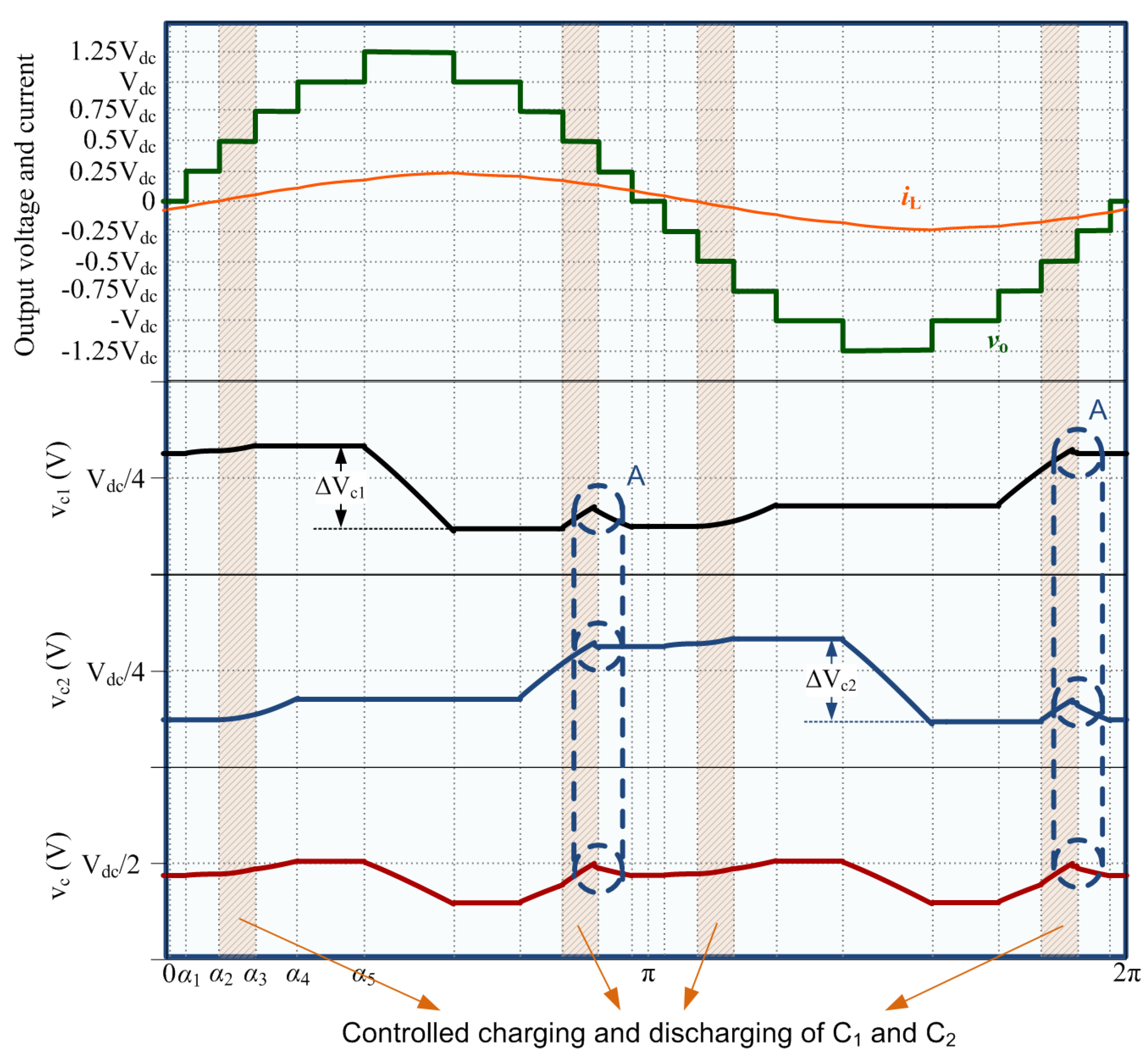
Figure 1 presents the evolution from [9,18], and the circuit schematic of the presented UXE-type 11-level inverter topology. The arrangement consist of a DC source and two capacitors C 1 and C 2 , six switches with antiparallel diodes, four switches without antiparallel diodes, and two switches connected in antiseries forming an AC-switch. Instead of capacitors in the auxiliary DC-link, batteries or PV source can be used. S 1 and S 1 along with the DC source forms U; S 2 , S 2 , S 3 , S 3 and S 4 , S 4 form an X; and S 5 , the AC-switch S 6 and S 7 forms the alphabet E. Thus, the inverter is named UXE-type inverter.
This topology produces a 1.25 boosted output using a single source. A single voltage sensor and across the auxiliary DC-link voltage a current sensor in the load path is sufficient to balance the voltages across the capacitors C 1 and C 2 .

2.2. Voltage Balancing of C 1 and C 2

Figure 2 exhibits the capacitors engaged in the formation of each level. The successful 11-level operation of the UXE inverter can be ascertained by maintaining the voltages of the capacitors of the auxiliary DC-link at V d c / 4 . For this, the redundant states available at the level of V d c / 2 and V d c / 2 are used (see Table 1 and Figure 3). Controlled charging and discharging at levels V d c / 2 , V d c / 2 can be achieved with either direction of current flowing through the capacitors.
Figure 4 shows the durations of charging and discharging of the capacitors C 1 and C 2 at various loads. It is apparent from the figure that the sufficient durations are available to maintain the individual capacitors at V d c / 4 by using the redundant states (available at V d c / 2 and V d c / 2 ). This will result in a DC-link voltage of V d c / 2 with V d c / 4 across each capacitor. Thus, only one voltage sensor is utilized to balance the voltage across the auxiliary DC-link instead of two sensors. The algorithm exhibited in Figure 5 is used to ensure a contained discharging and charging of the capacitors. The voltage ripple of C 1 and C 2 are shown in Figure 6. At A (shown in Figure 6) it is visualized that with the auxiliary DC-link voltage reaching V d c / 2 , the algorithm ascertains the redundant state’s activation according to Figure 5 and thus the capacitors discharge.
Further, the capacitor’s voltage ripple and the load current’s magnitude are used to find the value of the capacitors. The limit on the dip in the ripple is maintained at 5% of V d c / 4 . The change in the energy with a plunge of Δ V c 1 and Δ V c 2 in the capacitor voltages can be given as:
Δ Q c i = 1 2 C i Δ V c i
With a consideration of 5% ripple, the value of the capacitors can be defined as:
C i = 80 Q c i V d c
The energy of the capacitors is dependent on the load can be determined by the method utilized in [34]. The capacitors of 2500 μF are considered for this work.

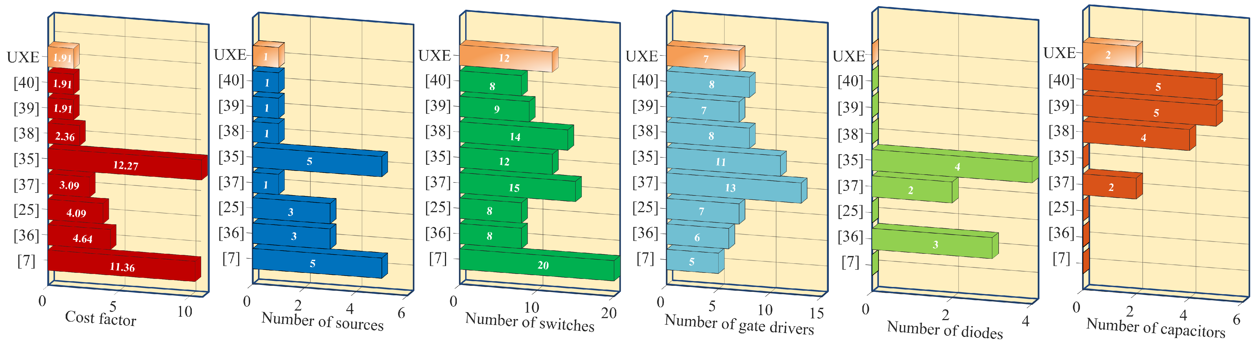
3. Comparison with Recent Inverters

The presented UXE-11 inverter is compared with recent 11-level inverters in this section. The analysis is performed according to the number of IGBTs ( N T ), number of sources ( N S ), gate driver circuits ( N d r ), passive elements ( N C and N L ), number of diodes ( N D ) and the cost factor (CF). The CF is a function of these parameters and is given as:
C F = N C + N L + N T + N d + N d r N s N l e v e l s
The comparison is presented in Figure 7 and Table 2. The topology introduced by Hassan et al. in [35] exhibits highest CF of 12.27 as it employs 5 sources. Moreover, some switches of higher PIV rating are required. The CHB by cascading 5 units will require 20 switches driven by 5 drivers and 5 same magnitude sources [7]. The larger amount of switches tends to a higher CF. However, this structure is still attractive due to its key feature of modularity. An 11-level topology presented by Tjokro et al. in [36] require 3 sources of different magnitudes, 8 switches and 3 diodes. Due to different sources, the boosting capability cannot be described in these inverters. Siddiqui et al. in [25] presents an 11-level topology driven by 3 sources and uses 8 switches and 7 gate drivers. A single-source topology is discussed by Babu et al. in [37] and uses 15 switches, 2 capacitors and 2 inductors as passive elements and 2 diodes, leading to a CF of 3.09. Karimi et al. [38] demonstrates a single-source topology using 14 switches that are driven by 8 driver circuits and 4 capacitors. Rooholahi et al. presents a single-source topology with nine switches driven by seven driver circuits in [39]. The circuit also requires 5 capacitors for a successful 11-level output, which leads to an additional cost of the inverter, and reduces reliability. A circuit using one source, 8 switches, 5 capacitors and 8 driver circuits is presented in [40]. This topology exhibits no boosting. In comparison to these MLIs, the UXE-11 inverter uses a single DC-source, two capacitors, 12 switches that are driven by 7 drivers, which results in a low CF of 1.91.

4. Modulation of the UXE-11 Inverter

The inverters are generally controlled by Pulse Width Modulation (PWM) techniques. The examples of high-switching frequency PWM techniques are sine-PWM and space-vector modulation. These methods exhibit a reduced efficiency due to higher switching losses, but are helpful in closed loop control of motor drive systems [7]. On the other hand, the low switching frequency methods like Nearest level control (NLC) and selective harmonic elimination (SHE) exhibit low switching losses and better low-order harmonic control. This work uses a modified NLC (MNLC) and SHE to generate 11-level voltage output of the inverter.

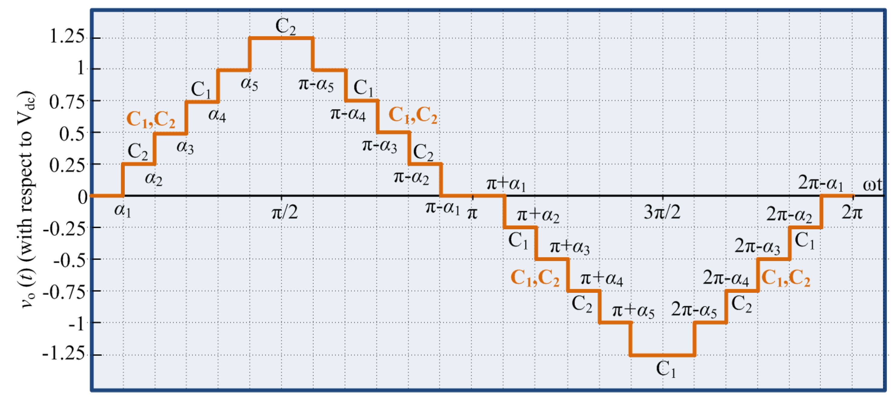
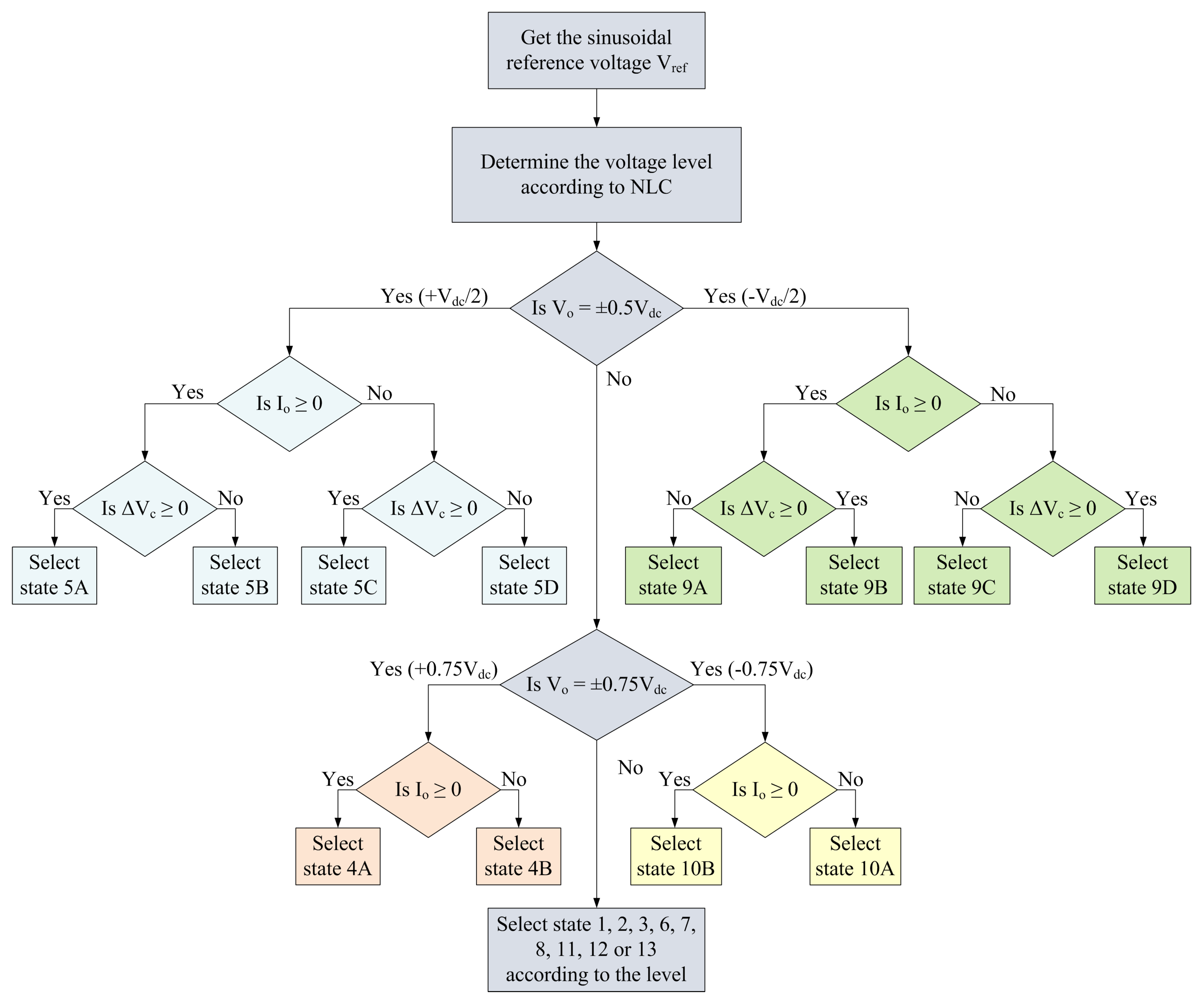
4.1. Nearest Level Control of UXE-11 Inverter

A modified NLC is applied to the converter by considering both zero states which. NLC ensures a near to sinusoid performance of the inverter ensuring a low lower order harmonic content in the voltage across the output terminals. The concept is exhibited pictorially in Figure 8. Firstly, the angles are yielded by comparison of the y-axis midpoints between the levels and the reference voltage V r e f . Then the switching of the inverter is ensured at these angles by applying the logical diagram shown in Figure 9. The definition of angles for 11-level operation is expressed as:
α j = sin 1 2 j 1 10
where, j < N / 2 and j is an index of the angle being calculated. The value of j will be lesser than the levels in one-quarter of a fundamental frequency cycle.
The midpoint signals L 1 to L 10 are shown in Figure 8. These signals in a general form are defined as:
L k = 1.35 0.25 k
where, k = 1 , 2 , , 10 . Further, in the Figure 8, The constant 0 generates a zeroth level L 0 . This in all leads to a formation of 11 signals namely D 0 to D 10 , exhibited in Figure 9. The signals are shown in red in Figure 8. The logical operations shown in Figure 9 synthesize the 11 states from state 0 to 10. Corresponding to conventionally employed NLC, here the operation is performed by application of both the zero states shown in Table 1. The two zero states are shown as 0 I and 0 I I in Figure 8 and Figure 9. This ensures equal amount of switching of the complementary operating switches. Finally, the gate driver are selected to drive the switches corresponding to these states.

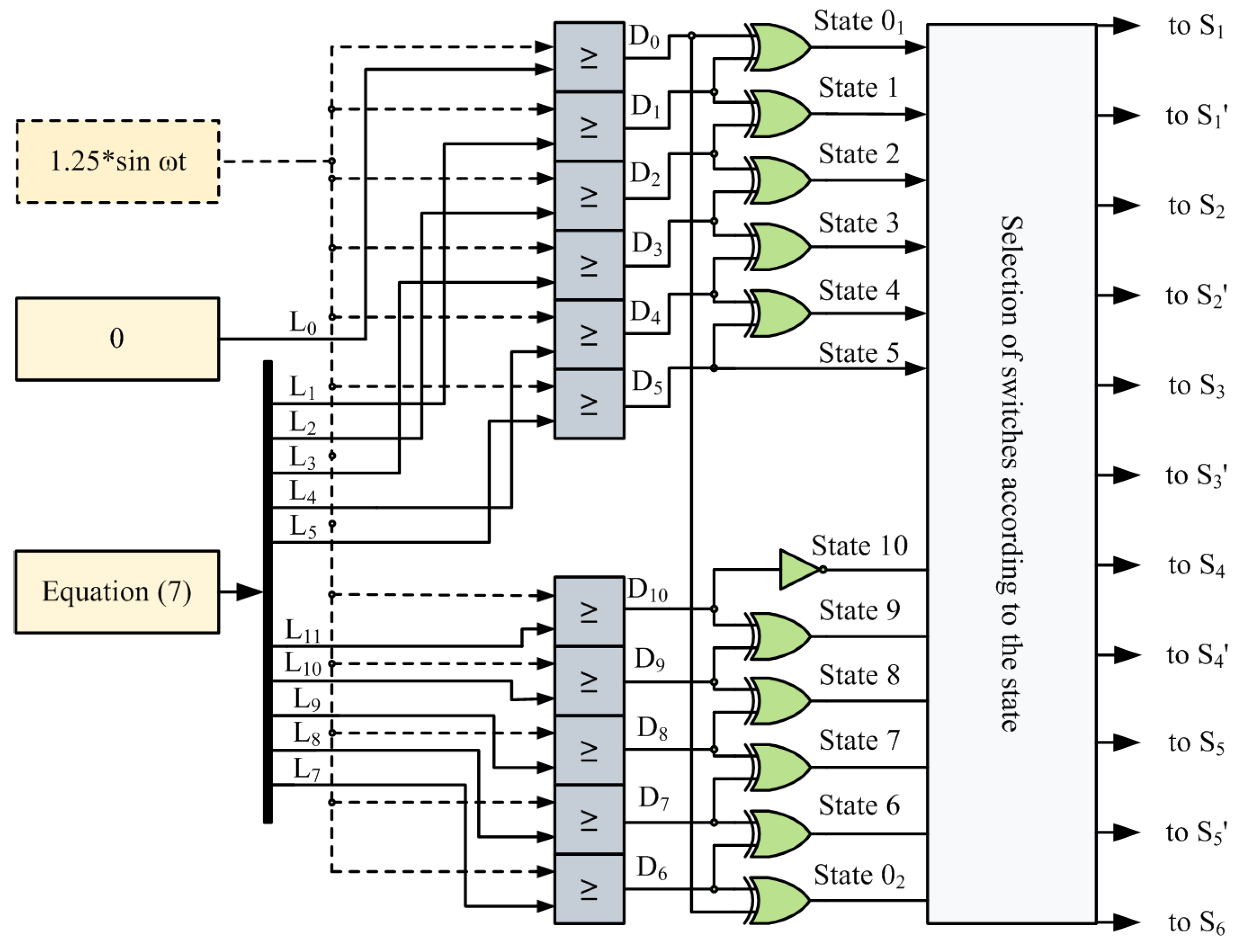
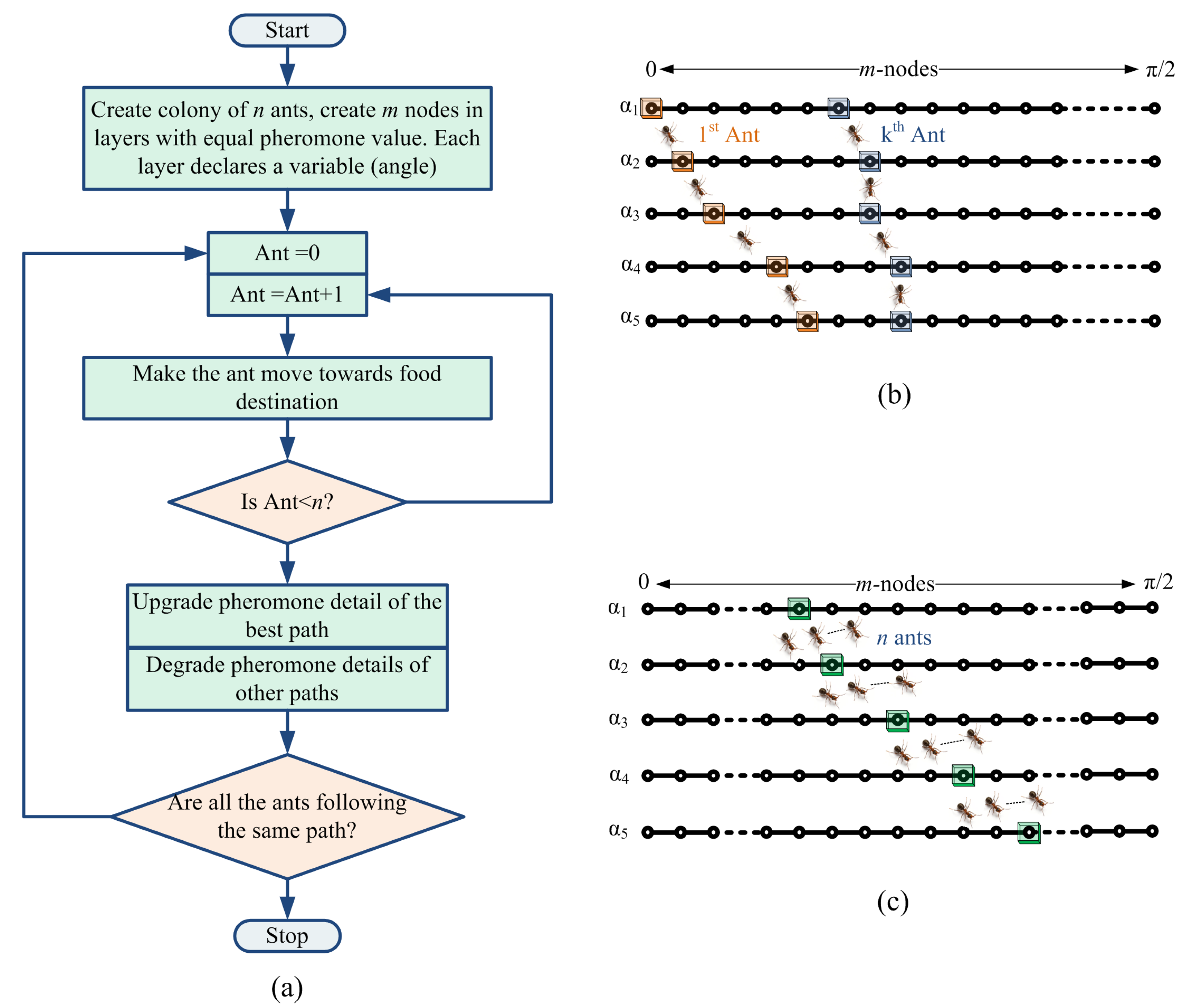
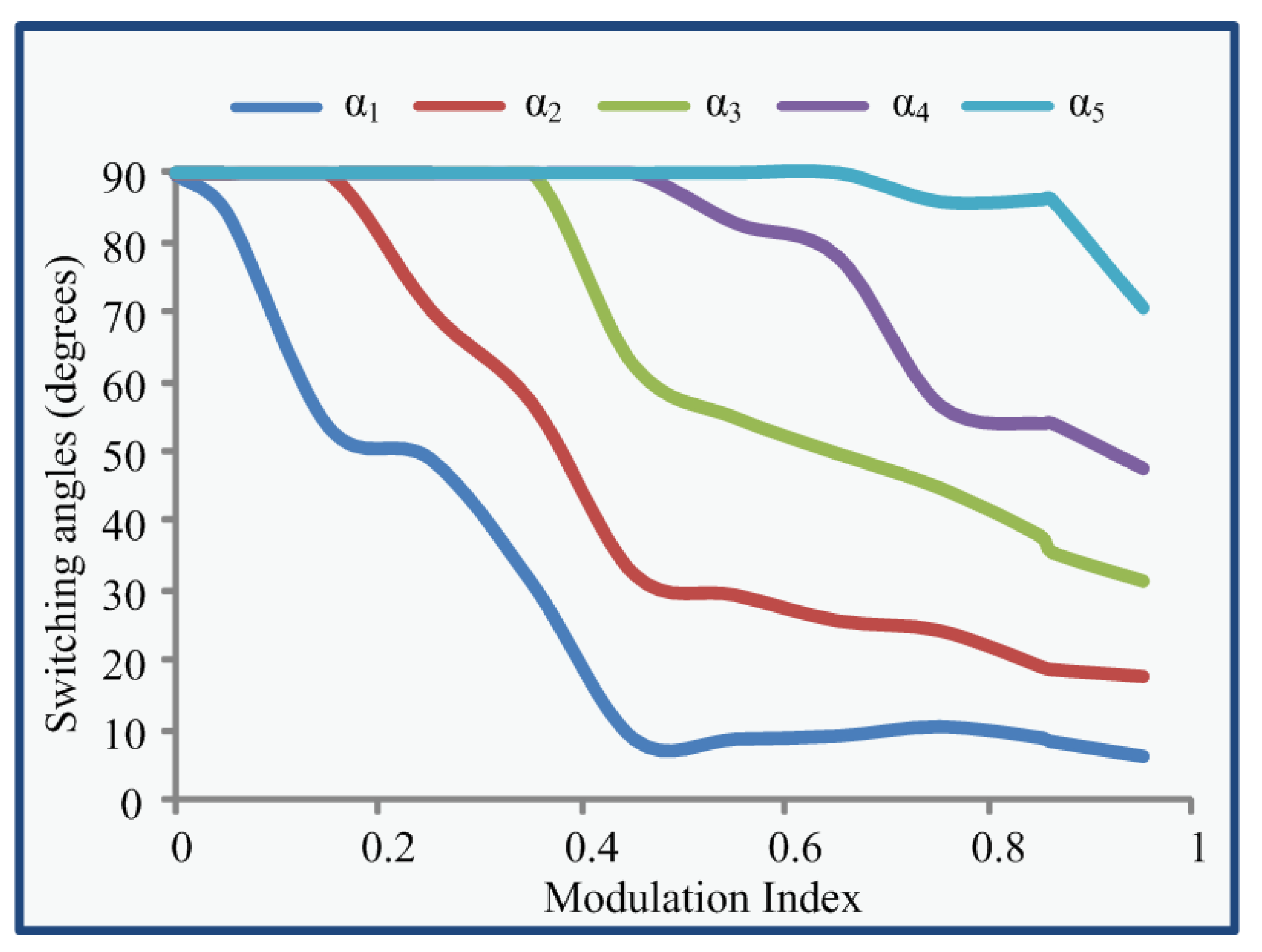
4.2. ACO-SHE Based Selective Harmonic Elimination

SHE is a low-switching frequency technique where the switching angles are selected to eliminate the low order harmonics in the output voltage waveform. Generally, m 1 harmonics are eliminated for m level operation. The angles can be derived by solving the transcendental equations. The solution of these equations are either based on mathematical analysis [28] or by using nature-inspired metaheuristic techniques [16]. In this work a swarm based ant colony optimization (ACO) technique is employed. The waveform shown in Figure 2 can be expanded as a Fourier expression:
v o ( θ ) = n = 0 A n cos θ + B n sin θ + A o
where, θ = ω t ; A n , B n and A o are the coefficients of even harmonics, the odd harmonics and the DC component, respectively. In the modulation strategy it is ensured that half-wave symmetry and quarter-wave symmetry are preserved to eliminate the even harmonics and the DC component. The expression can now be written as:
v o ( θ ) = n = 0 B n sin θ
where, B n is:
B n = 4 V d c n π j = 1 , 3 , 5 m cos n α j
As five angles are the tunable parameters, the control over the selected four harmonic voltages and the fundamental can be achieved. As the lower harmonics are to be eliminated, here 3rd, 5th, 7th and 9th harmonic voltages are chosen for elimination. The transcendental expressions are derived from (8) as follows:
cos α 1 + cos α 2 + cos α 3 + cos α 4 + cos α 5 = V d m a x π 4 V d c cos 3 α 1 + cos 3 α 2 + cos 3 α 3 + cos 3 α 4 + cos 3 α 5 = 0 cos 5 α 1 + cos 5 α 2 + cos 5 α 3 + cos 5 α 4 + cos 5 α 5 = 0 cos 7 α 1 + cos 7 α 2 + cos 7 α 3 + cos 7 α 4 + cos 7 α 5 = 0 cos 9 α 1 + cos 9 α 2 + cos 9 α 3 + cos 9 α 4 + cos 9 α 5 = 0
where, V d m a x is the desired fundamental voltage’s peak value. Further, for multiple modulation index operation:
M I = π V d m a x 2 × N l e v e l s m a x 1 × V d c
where, N l e v e l s m a x are the maximum levels achieved by an inverter, which is 11 here. The solution of the expressions is performed under constraints which are expressed as follows:
0 < α 1 < α 2 < α 3 < α 4 < α 5 < π / 2
Ant colony optimization (ACO) is a search based algorithm that is inspired by ant’s food searching behavior. Ants choose the shortest path to reach their food, and this feature was utilized as an optimization tool by Dorigo in [41]. The algorithm is depicted in Figure 10a. The variables to be determined are arranged in layers as array of solutions to the objective function, with each layer dedicated to a variable. Initially, each node of the array in the layer can be a solution; and thus each node is given equal probability of being a solution to the minimization problem. This probability is defined as pheromone in ACO, which is named due to its resemblance with the natural pheromone deposited by natural ants while searching their food. The optimization problem is a minimization function developed from (9), whose behavior is constrained by (11).
In the initial step, the ants are allowed to randomly choose a node in all the layers as shown in Figure 10b. While moving across the layers, the ants leave a trail by enhancement of the pheromone quantity. All the paths (or solutions) are tested for their fitness towards the objective function. The solution that produces minimum value gets the priority and the pheromone of its paths are enhanced. Meanwhile, the other path’s pheromones are degraded, which is also known as pheromone evaporation. The probability (or the pheromone quantity) is not rendered zero as there is still a possibility of having solutions in those paths. This single iteration is repeated multiple times till the ants follow the most optimized trail as shown in Figure 10c.
The code for ACO algorithm was written in MATLAB. The required five angles were obtained as solution of the algorithm. The angles were derived for a wide spectrum of MI from 0 to 1. The optimum angles with respect to modulation index (MI) are developed as Figure 11.

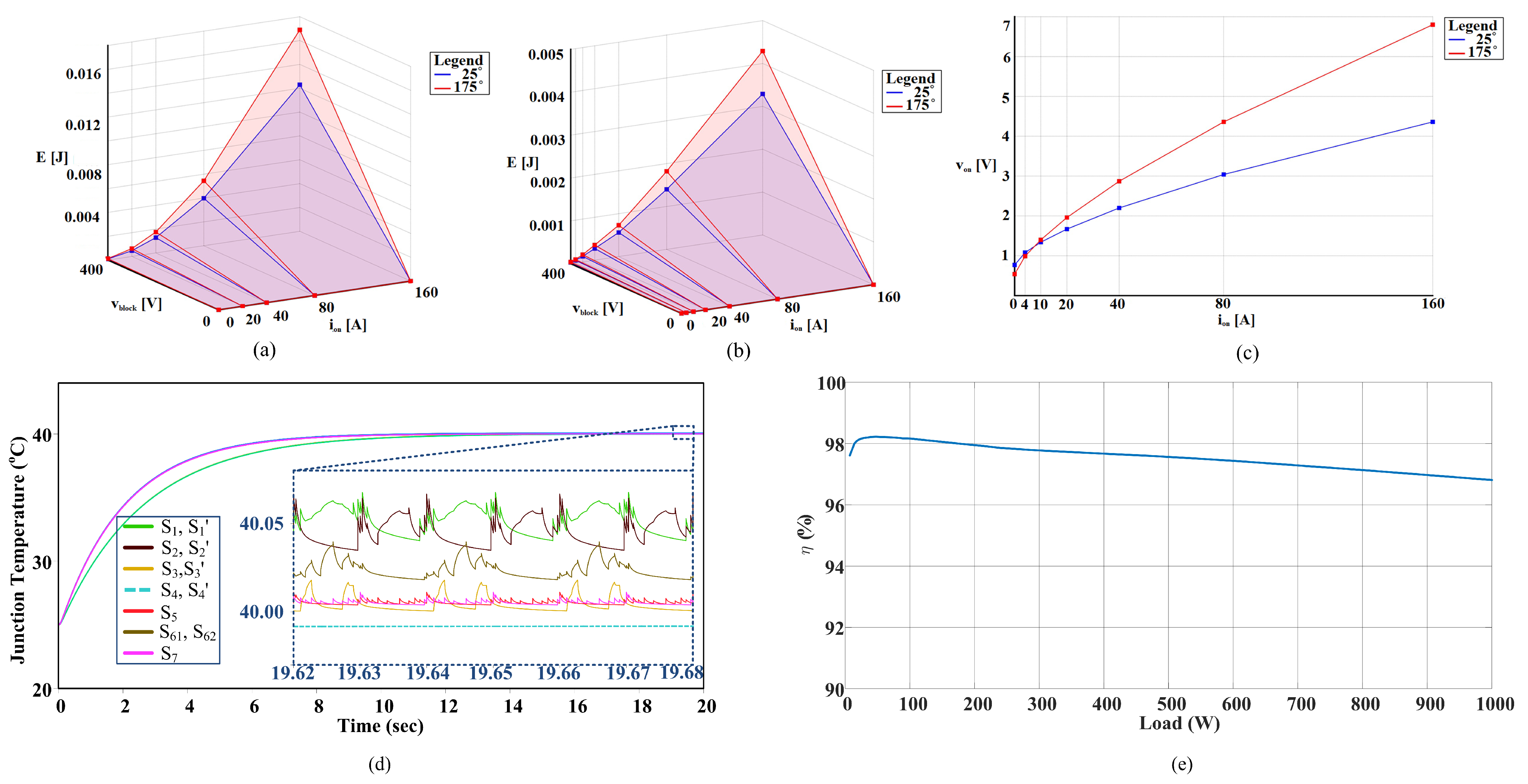
5. Analysis of Power Loss

The analysis of power loss includes the losses occurring during conduction of the diodes and switches, and, their switching losses. The analysis of these losses is presented analytically and in the PLECS software.

5.1. Switching Losses

Switching losses occur due the turn-on and turn-off of the switches and diodes. For a singe switch, the turn-on loss is defined as:
e i o n = 0 t o n v ( t ) i ( t ) d t = 0 t o n V s i t o n I o n t o n t o n t = 1 6 V s i t o n 2 I o n .
Similarly, during the turning-off condition:
e i o f f = 0 t o f f v ( t ) i ( t ) d t = 0 t o f f V s i t o f f I o f f t o f f t o f f t = 1 6 V s i t o f f 2 I o f f
where, I o f f and I o n define the currents before and after the turning-off and turning-on of the switch, respectively. V s i is the voltage across the switch during turning-off state. The total switching loss is thus:
P s w = 1 T i = 1 N s w i t c h j = 1 N i o n e i j o n + j = 1 N i o f f e i j o f f .

5.2. Conduction Losses

Conduction losses are ohmic losses occurring during the conduction of the semiconductor devices. It can be defined as:
e P c i = R s i γ ( t ) + V s i ( t )
where, V s is the on-state voltage drop, R s is the switch’s resistance and, γ is a constant described in the switch’s data sheet. This loss is now described as follows:
P c = 1 T 0 2 π i = 1 N s w i t c h P c i ( t ) .
The total losses of the converter are finally found as:
P l o s s = P c + P s w .
The losses of the inverter are determined by using the PLECS software. The analysis is performed by employing IKFW50N60DH3E-IGBT model. Figure 12a,b exhibit the turning-on and turning-off losses relative to V s i and I o n . Figure 12c presents the relationship of the conduction loss with the on-state conduction current ( I o n ). Figure 12d exhibits the temperature of the switches’ junction at 40 °C. Figure 12e exhibits the inverter’s efficiency curve, where the maximum efficiency is found to be 98.1%.

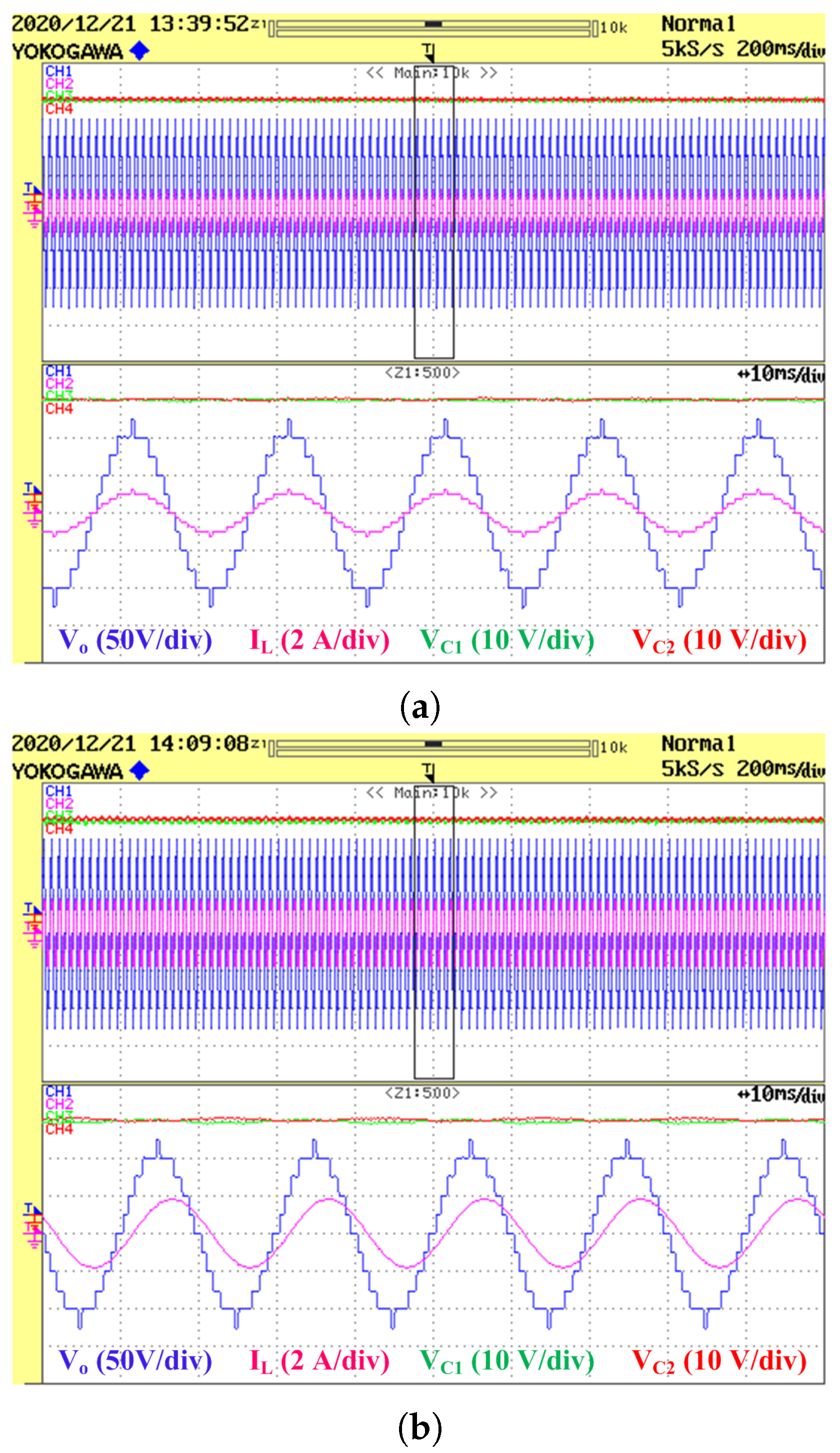
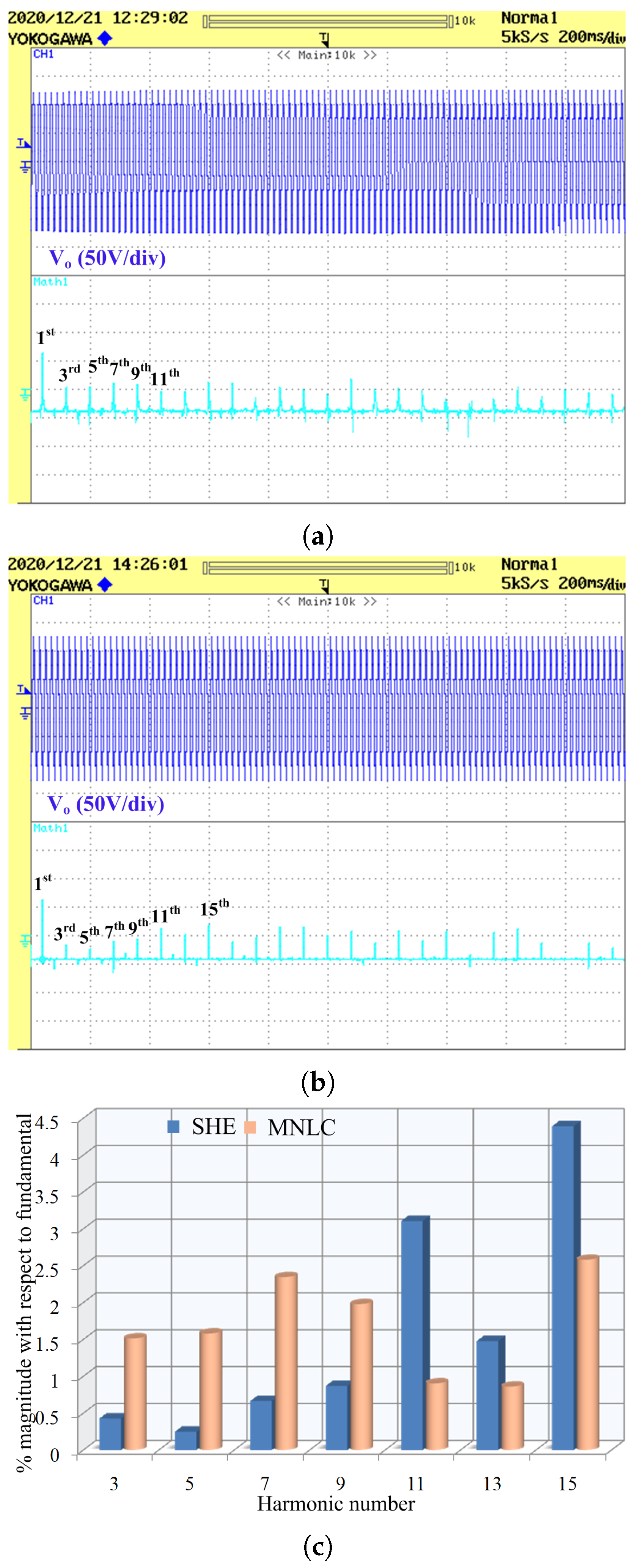
6. Hardware-in-the-Loop Validation

The investigation of the UXE-11 inverter is performed on various loading conditions with NLC and ACO-SHE modulation. The SHE is performed at 0.85 modulation index. Both the methods are validated on the HIL platform of Typhoon. For the SHE, the inverter is switched after the determined of angles in offline mode, as discussed in Section 4.2. The DC-source magnitude is taken as 100 V. During the operation of the inverter, the voltage balance algorithm (Figure 5) must be capable of maintaining 50 V across the capacitor bank, and 25 V each across both the capacitors. A voltage with 125 V peak with a boosting of 1.25 will be achieved. The DC-link capacitors of 2500 μF, 50 V and 0.001 Ω ESR is used. The parameters are also shown in Table 3.
The inverter’s behavior with 50 Ω (R-load) is shown in Figure 13a. The initial behavior suggests that with capacitors completely discharged, 100 V (or V d c ) will appear at the output. With time, as the capacitor’s value attain 25 V, the DC-link voltage of 50 V is achieved, as desired. The capacitor voltages are recoded with a 0.5 division offset for better visibility. Figure 13b exhibits inverter performance with 50 Ω, 100 mH and at 0.94 modulation index. This forms a load of approximately 0.8 lagging power factor. Figure 13c shows the output and capacitor behavior with a load changing from 50 Ω to 100 Ω, 100 mH. As visible, the capacitor’s voltages have a higher ripple at the starting of the change, but it comes down with steady state condition of the capacitors is reached. Moreover, the ripple content is more prominent with the inductive load compared to purely resistive load, suggesting that the ripple behavior depends on the type of load employed.
The results with the SHE operation of UXE-type inverter with R-load of 100 Ω are shown in Figure 14a. Similarly, the operation of the inverter with RL-load of 50 Ω, 100 mH is shown in Figure 14a. The fast Fourier transform (FFT) analysis of the voltage waveforms with the MNLC and SHE are shown in Figure 15. Figure 15a,b shows the FFT of the voltgae wavefrom with the MNLC and SHE. The harmonics are marked from the fundamental to the 11th harmonic. With SHE, the 15th harmonic has the highest value. The values in the oscilloscope are in dBV. The conversion of these values in volts (peak) are shown in Table 4. The comparison of these harmonics with both techniques is shown in Figure 15c. The figure suggests that the low-order harmonics, i.e., 3rd, 5th, 7th and 9th are lower than 1% and also lower than the MNLC. These harmonics were controlled by employing optimum angles obtained from ACO technique. Further, with the increment in harmonic number, the magnitude of the harmonics in SHE is more than the MNLC. This suggests that although the lower order harmonics are controlled by SHE, the energy is transferred to higher order harmonics.

7. Conclusions

In this work, the UXE inverter was considered for 11-level operation. Its detailed circuit analysis consisting of a single DC-source with 12 semiconductor switches was presented. The UXE-11 inverter’s comparison with recent eleven level topologies showed that the topology has a low cost factor. The algorithm using the redundant states was defined to balance the voltage across the DC-link around V d c / 2 under permissible ripple. The 11-level operation using this algorithm was successfully implemented on the inverter in the Typhoon HIL environment using two switching methods. The first method was the nearest level control in which both zero states of the converter were used. Moreover, the other method was the selective harmonic elimination where the ant colony optimization technique was utilized to find the instances of switching. The magnitudes of each lower order harmonic in voltage and current were less than the permissible limit of 1% after their elimination. The inverter’s loss analysis was performed on the PLECS environment with the inverter’s maximum efficiency achieved at 98.1%.
A low-switch count single-phase topology is investigated, which produces 11-level operation. The topology and its modulation strategy result in better output AC waveforms with low hardware investment compared to conventional large-device count topologies. This topology can be effectively considered for low-voltage renewable energy integration and electrical vehicle chargers.

Author Contributions

Conceptualization, M.A. and M.T.; methodology, M.A. and M.T.; Writing-original draft, M.A. and B.A.; Writing—review and editing, M.A., C.-H.L., R.K.C., M.J.R., A.A.; visualization, M.A.; supervision, M.T and R.K.C. All authors contributed collectively to the manuscript preparation. All authors have read and agreed to the published version of the manuscript.

Funding

The authors would like to acknowledge the financial support from Taif University Researchers Supporting Project Number (TURSP-2020/121), Taif University, Taif, Saudi Arabia; and in part from the Collaborative Research Grant Scheme (CRGS) Project CRGS/MOHD TARIQ/01 sponsored by the Capability Systems Centre, UNSW, Canberra to the Hardware-In-the-Loop (HIL) Lab, Department of Electrical Engineering, Aligarh Muslim University, India and from the Ministry of Science and Technology, Taiwan, R.O.C., grant number MOST 110-2221-E-011-081, MOST 110-2622-E-011-004.

Institutional Review Board Statement

Not applicable.

Informed Consent Statement

Not applicable.

Acknowledgments

The authors acknowledge the technical support provided by the Hardware-In-the-Loop (HIL) Lab, Department of Electrical Engineering, Aligarh Muslim University, India.

Conflicts of Interest

The authors declare no conflict of interest.

References

  1. Mishra, N.; Singh, B. Modified reduced switch converter for grid interfaced systems. In Proceedings of the 2018 IEEE Industry Applications Society Annual Meeting (IAS), Portland, OR, USA, 23–27 September 2018; pp. 1–8. [Google Scholar] [CrossRef]
  2. Salem, A. Design, implementation and control of a SiC-Based T5MLC induction drive system. IEEE Access 2020, 8, 82769–82780. [Google Scholar] [CrossRef]
  3. Gupta, K.K.; Ranjan, A.; Bhatnagar, P.; Sahu, L.K.; Jain, S. Multilevel Inverter Topologies with Reduced Device Count: A Review. IEEE Trans. Power Electron. 2016, 31, 135–151. [Google Scholar] [CrossRef]
  4. Kouro, S.; Malinowski, M.; Gopakumar, K.; Pou, J.; Franquelo, L.G.; Wu, B.; Rodriguez, J.; Member, S.; Pérez, M.A.; Leon, J.I. Recent Advances and Industrial Applications of Multilevel Converters. IEEE Trans. Ind. Electron. 2010, 57, 2553–2580. [Google Scholar] [CrossRef]
  5. Lai, J.S.; Peng, F.Z. Multilevel Converters-A New Breed of Power Converters. IEEE Trans. Ind. Appl. 1996, 32, 509–517. [Google Scholar] [CrossRef]
  6. Bana, P.R.; Panda, K.P.; Naayagi, R.T.; Siano, R.; Panda, G. Recently Developed Reduced Switch Multilevel Inverter for Renewable Energy Integration and Drives Application: Topologies, Comprehensive Analysis and Comparative Evaluation. IEEE Access 2019, 7, 54888–54909. [Google Scholar] [CrossRef]
  7. Malinowski, M.; Gopakumar, K.; Rodriguez, J.; Perez, M.A. A survey on cascaded multilevel inverters. IEEE Trans. Ind. Electron. 2010, 57, 2197–2206. [Google Scholar] [CrossRef]
  8. Salem, A.; Khang, H.V.; Robbersmyr, K.G.; Norambuena, M.; Rodriguez, J. Voltage Source Multilevel Inverters with Reduced Device Count: Topological Review and Novel Comparative Factors. IEEE Trans. Power Electron. 2021, 36, 2720–2747. [Google Scholar] [CrossRef]
  9. Ounejjar, Y.; Al-Haddad, K.; Grégoire, L.A. Packed U Cells Multilevel Converter Topology: Theoretical Study and Experimental Validation. IEEE Trans. Ind. Electron. 2011, 58, 1294–1306. [Google Scholar] [CrossRef]
  10. Vahedi, H.; Sharifzadeh, M.; Al-Haddad, K. Modified Seven-Level Pack U-Cell Inverter for Photovoltaic Applications. IEEE J. Emerg. Sel. Top. Power Electron. 2018, 6, 1508–1516. [Google Scholar] [CrossRef]
  11. Mohamed Ali, J.S.; Krishnasamy, V. Compact Switched Capacitor Multilevel Inverter (CSCMLI) with Self-Voltage Balancing and Boosting Ability. IEEE Trans. Power Electron. 2019, 34, 4009–4013. [Google Scholar] [CrossRef]
  12. Siddique, M.D.; Sathik, J.M.A.; Mekhilef, S.; Mustafa, A.; Sandeep, N.; Almakhles, D. Reduce Switch Count Based Single Source 7L Boost Inverter Topology. IEEE Trans. Circuits Syst. II Express Briefs 2020, 67, 3252–3256. [Google Scholar] [CrossRef]
  13. Roy, T.; Sadhu, P.K.; Dasgupta, A. Cross-Switched Multilevel Inverter Using Novel Switched Capacitor Converters. IEEE Trans. Ind. Electron. 2019, 66, 8521–8532. [Google Scholar] [CrossRef]
  14. Saeedian, M.; Adabi, M.E.; Hosseini, S.M.; Adabi, J.; Pouresmaeil, E. A Novel Step-Up Single Source Multilevel Inverter: Topology, Operating Principle, and Modulation. IEEE Trans. Power Electron. 2019, 34, 3269–3282. [Google Scholar] [CrossRef] [Green Version]
  15. Siddique, M.D.; Mekhilef, S.; Shah, N.M.; Sarwar, A.; Tayyab, M.; Ansari, M.K. Low Switching Frequency Based Asymmetrical Multilevel Inverter Topology with Reduced Switch Count. IEEE Access 2019, 7, 86374–86383. [Google Scholar] [CrossRef]
  16. Lodi, K.A.; Ali, M.; Tariq, M.; Meraj, M.; Iqbal, A.; Chakrabortty, R.K.; Ryan, M.J. Modulation with Metaheuristic Approach for Cascaded-MPUC49 Asymmetrical Inverter with Boosted Output. IEEE Access 2020, 8, 96867–96877. [Google Scholar] [CrossRef]
  17. Mishra, N.; Yadav, S.K.; Singh, B.; Padmanaban, S.; Blaabjerg, F. Binary-Quintuple Progression Based Twelve Switch Twenty-Five Level Converter with Nearest Level Modulation Technique for Grid-Tied and Standalone. IEEE Trans. Ind. Appl. 2020, 57, 3214–3223. [Google Scholar] [CrossRef]
  18. Sharifzadeh, M.; Al-Haddad, K. Packed E-Cell (PEC) Converter Topology Operation and Experimental Validation. IEEE Access 2019, 7, 93049–93061. [Google Scholar] [CrossRef]
  19. Kim, K.M.; Han, J.K.; Moon, G.W. A High Step-Up Switched-Capacitor 13-Level Inverter with Reduced Number of Switches. IEEE Trans. Power Electron. 2020, 36, 2505–2509. [Google Scholar] [CrossRef]
  20. Sotoodeh, P.; Miller, R.D. Design and implementation of an 11-level inverter with FACTS capability for distributed energy systems. IEEE J. Emerg. Sel. Top. Power Electron. 2014, 2, 87–96. [Google Scholar] [CrossRef]
  21. Saggu, T.S.; Singh, L.; Gill, B.; Member, S. Harmonics Mitigation in a Steel Industry Using 11-Level Cascaded Multilevel Inverter-Based DSTATCOM. Can. J. Electr. Comput. Eng. 2017, 40, 110–115. [Google Scholar]
  22. Routray, A.; Kumar Singh, R.; Mahanty, R. Harmonic Minimization in Three-Phase Hybrid Cascaded Multilevel Inverter Using Modified Particle Swarm Optimization. IEEE Trans. Ind. Inform. 2019, 15, 4407–4417. [Google Scholar] [CrossRef]
  23. Routray, A.; Singh, R.K.; Mahanty, R. Harmonic Reduction in Hybrid Cascaded Multilevel Inverter Using Modified Grey Wolf Optimization. IEEE Trans. Ind. Appl. 2020, 56, 1827–1838. [Google Scholar] [CrossRef]
  24. Shuvo, S.; Hossain, E.; Islam, T.; Akib, A.; Padmanaban, S.; Khan, M.Z.R. Design and Hardware Implementation Considerations of Modified Multilevel Cascaded H-Bridge Inverter for Photovoltaic System. IEEE Access 2019, 7, 16504–16524. [Google Scholar] [CrossRef]
  25. Siddique, M.D.; Mekhilef, S.; Shah, N.M.; Memon, M.A. Optimal Design of a New Cascaded Multilevel Inverter Topology with Reduced Switch Count. IEEE Access 2019, 7, 24498–24510. [Google Scholar] [CrossRef]
  26. Sharifzadeh, M.; Babaie, M.; Sebaaly, F.; Mehrasa, M.; Chouinard, G.; Al-Haddad, K. Low Switching Frequency Operation of PEC9 Multilevel Inverter Using Modified SHM-PWM. In Proceedings of the IECON 2020: The 46th Annual Conference of the IEEE Industrial Electronics Society, Singapore, 18–21 October 2020; pp. 4215–4220. [Google Scholar]
  27. Taheri, A.; Rasulkhani, A.; Ren, H.P. An Asymmetric Switched Capacitor Multilevel Inverter with Component Reduction. IEEE Access 2019, 7, 127166–127176. [Google Scholar] [CrossRef]
  28. Al-Hitmi, M.; Ahmad, S.; Iqbal, A.; Padmanaban, S.; Ashraf, I. Selective Harmonic Elimination in a Wide Modulation Range using Modified Newton-Raphson and Pattern Generation Methods for a Multilevel Inverter. Energies 2018, 11, 458. [Google Scholar] [CrossRef] [Green Version]
  29. Lodi, K.A.; Azeem, A.; Tariq, M.; Ali, M.; Bharatiraja, C. Harmonic Minimization in Modified PUC-5 Inverter Using Genetic Algorithm. In Proceedings of the 2018 IEEE International Conference on Power Electronics, Drives and Energy Systems (PEDES), Chennai, India, 18–21 December 2018; pp. 1–6. [Google Scholar] [CrossRef]
  30. Ali, M.; Iqbal, A.; Anees, M.A.; Khan, M.R.; Rahman, K.; Ayyub, M. Differential evolution-based pulse-width modulation technique for multiphase MC. IET Power Electron. 2019, 12, 2224–2235. [Google Scholar] [CrossRef]
  31. Tayyab, M.; Sarwar, A.; Tariq, M.; Chakraborty, R.K.; Ryan, M.J. Hardware-In-the-Loop Implementation of projectile target search algorithm for selective harmonic elimination in a 3-phase multilevel converter. IEEE Access 2020, 9, 30626–30635. [Google Scholar] [CrossRef]
  32. Dorigo, M.; Gambardella, L.M.; Martinoli, M.; Poli, R.; Stützle, T. Ant Colony Optimization and Swarm Intelligence. In Proceedings of the 5th International Workshop, ANTS 2006, Brussels, Belgium, 4–7 September 2006. [Google Scholar]
  33. Zhang, Y.; Hu, C.; Wang, Q.; Zhou, Y.; Sun, Y. Neutral-point potential balancing control strategy for three-level ANPC converter using SHEPWM scheme. Energies 2019, 12, 4328. [Google Scholar] [CrossRef] [Green Version]
  34. Samadaei, E.; Kaviani, M.; Bertilsson, K. A 13-Levels Module (K-Type) with Two DC Sources for Multilevel Inverters. IEEE Trans. Ind. Electron. 2019, 66, 5186–5196. [Google Scholar] [CrossRef]
  35. Hassan, A.M.M.; Yang, X.; Ali, A.I.M. A Study of Level- Shifted PWM Single-phase 11-Level Multilevel Inverter. In Proceedings of the 21st International Middle East Power Systems Conference (MEPCON), Cairo, Egypt, 17–19 December 2019; pp. 170–176. [Google Scholar]
  36. Tjokro, C.; Pratomo, L.H. Design and Simulation of an Asymmetrical 11-Level Inverter for Photovoltaic Applications. In Proceedings of the 2018 5th International Conference on Information Technology, Computer, and Electrical Engineering (ICITACEE), Semarang, Indonesia, 27–28 September 2018; pp. 93–98. [Google Scholar] [CrossRef]
  37. Babu, S.M.; Narasimharaju, B.L.; Rathore, A.K. New Single-Stage Boost Multilevel Inverter. In Proceedings of the 2019 IEEE Transportation Electrification Conference (ITEC-India), Bengaluru, India, 17–19 December 2019; pp. 1–4. [Google Scholar]
  38. Karimi, M.; Kargar, P.; Varesi, K. A Novel High-Gain Switched-Capacitor Based 11- Level Inverter Topology. In Proceedings of the 2019 International Power System Conference (PSC), Tehran, Iran, 9–11 December 2019; pp. 404–409. [Google Scholar] [CrossRef]
  39. Rooholahi, B. A New Transformerless Single-Phase Eleven-Level Inverter with Reduction of Switches Based on Model Predictive Control Method. In Proceedings of the 2020 2nd Global Power, Energy and Communication Conference (GPECOM), Izmir, Turkey, 20–23 October 2020; pp. 102–107. [Google Scholar]
  40. Shahrukh, M.; Usmani, A.A.; Shrivastava, P.; Kidwai, S. New Single Phase 11 Level Inverter Topology usng Multilevel PWM Switching with Lesser Components Count. In Proceedings of the 2018 IEEE Texas Power and Energy Conference (TPEC), College Station, TX, USA, 8–9 February 2018; pp. 1–6. [Google Scholar]
  41. Dorigo, M. Optimization, Learning and Natural Algorithms. Ph.D. Thesis, Politecnico di Milano, Milan, Italy, 1992. [Google Scholar]
Figure 1. The evolution of presented Inverter: (a) The 5-level PUC [9], (b) The 9-level PEC [18], and (c) the presented UXE-11 topology.
Sustainability 13 09035 g001
Figure 2. Eleven-level stepped waveform of the UXE-11 inverter with the capacitors engaged in level formation.
Sustainability 13 09035 g002
Figure 3. All the states of the 11-level UXE-type Inverter.
Sustainability 13 09035 g003
Figure 4. Capacitor C 1 and C 2 charging and discharging states with (a) resistive, (b) inductive and (c) capacitive loads.
Sustainability 13 09035 g004
Figure 5. Flowchart to exhibit the algorithm used to control the charging and discharging of C 1 and C 2 .
Sustainability 13 09035 g005
Figure 6. Capacitors C 1 and C 2 voltages with MNLC operation of the inverter.
Sustainability 13 09035 g006
Figure 7. Graphical representation of the comparison of UXE-11 inverter with 11-level topologies.
Sustainability 13 09035 g007
Figure 8. Pulse generation in the modified nearest level control.
Sustainability 13 09035 g008
Figure 9. Logical diagram to generate pulses modified nearest level control.
Sustainability 13 09035 g009
Figure 10. (a) Flowchart of ACO, (b) initial stage of ants, and (c) final stage of ants.
Sustainability 13 09035 g010
Figure 11. Variation in switching angles produced by ACO with variation in modulation index.
Sustainability 13 09035 g011
Figure 12. IGBT (a) Turning-on characteristics, (b) Turning-off characteristics, (c) Conduction losses, (d) Switch junction temperatures at 40 °C, and (e) Inverter efficiency curve.
Sustainability 13 09035 g012
Figure 13. Results exhibiting the output voltage, load current and voltages across C 1 and C 2 with (a) R-load of 100 Ω, (b) RL load of 50 Ω, 100 mH, (c) loading change from 50 Ω, 100 mH to 100 Ω, 100 mH.
Sustainability 13 09035 g013
Figure 14. Results exhibiting the output voltage, load current and, voltages across C 1 and C 2 with SHE with (a) R-load (100 Ω), and (b) RL-load (50 Ω, 100 mH), at modulation index of 0.86.
Sustainability 13 09035 g014
Figure 15. Results showing FFT of the the output voltage (a) with MNLC, and (b) SHE, and; (c) comparison of lower order harmonics with both techniques.
Sustainability 13 09035 g015
Table 1. The presented UXE-11 Inverter states.
State S 1 S 1 S 2 S 2 S 3 S 3 S 4 S 4 S 5 S 6 S 7 V o I o C 1 C 2
1A.100100000101.25E+D-
1B.100100000101.25EC-
2A.10010000001E+--
2B.10010000001E--
3A.100010000100.75E+-C
3B.100000100100.75E-D
4A.100010000010.5E+CC
4B.010100001000.5E+DD
4C.010100001000.5ECC
4D.100000100010.5EDD
5A.010100000100.25E+D-
5B.010100000100.25EC-
6A.101000001000--
6B.010100000010--
7A.10100000010−0.25E+-C
7B.10100000010−0.25E-D
8A.10100000001−0.5E+CC
8B.01000001100−0.5E+DD
8C.01000100100−0.5ECC
8D.10100000001−0.5EDD
9A.01000100010−0.75EC-
9B.01000001010−0.75E+D-
10A.01100000100−E+--
10B.01100000100−E--
11A.01100000010−1.25E+-D
11B.01100000010−1.25E-C
E = V d c , D = discharging, C = charging, and - = neither charging nor discharging.
Table 2. Comparison of UXE-11 with 11-level MLIs.
MLI N level N S N T N D N dr N C N L BC CF
[35]1151241100ND12.27
CHB [7]115200500No11.36
[36]11383600ND4.64
[25]11380700ND4.09
[37]1111521322Yes3.09
[38]111140840Yes2.36
[39]11190750No1.91
[40]11180850No1.91
[11]91110920Yes2.44
UXE-11121110720Yes1.91
N L = number of inductors, N C = number of capacitors, N D = not defined, BC = boosting capability.
Table 3. Table of parameters.
S. No.ParametersValue
1.DC-Source Voltage100 V
2.Capacitors2500 μF, 50 V
3.Resistive Load50 & 100 Ω
4.Inductive Load100 mH
5.Power frequency50 Hz
Table 4. Analysis of FFT of voltages with MNLC and SHE.
MI α 1 α 2 α 3 α 4 α 5
0.868.46118.94135.82254.19586.228
FFT analysis with MNLC (MI = 0.94)
Unit1st3rd5th7th9th
dBV38.5452.1482.5205.9474.4727
Peak (V)119.611.8111.8902.80462.367
FFT analysis with SHE (MI = 0.86)
dBV37.734−9.627−14.336−5.8008−3.477
peak (V)108.950.4670.2720.7250.947
Publisher’s Note: MDPI stays neutral with regard to jurisdictional claims in published maps and institutional affiliations.

