Review

Delamination-and Electromigration-Related Failures in Solar Panels—A Review

by
Abdulwahab A. Q. Hasan
1,
Ammar Ahmed Alkahtani
1,*,
Seyed Ahmad Shahahmadi
1,
Mohammad Nur E. Alam
2,
Mohammad Aminul Islam
3 and
Nowshad Amin
1
1
Institute of Sustainable Energy, Universiti Tenaga Nasional, Jalan IKRAM-UNITEN, Kajang 43000, Selangor, Malaysia
2
School of Science, Edith Cowan University, 270 Joondalup Drive, Joondalup, WA 6027, Australia
3
Department of Electrical Engineering, Faculty of Engineering, University of Malaya, Jalan Universiti, Kuala Lumpur 50603, Selangor, Malaysia
*
Author to whom correspondence should be addressed.
Sustainability 2021, 13(12), 6882; https://doi.org/10.3390/su13126882
Submission received: 13 April 2021 / Revised: 1 June 2021 / Accepted: 6 June 2021 / Published: 18 June 2021

Abstract

:
The reliability of photovoltaic (PV) modules operating under various weather conditions attracts the manufacturer’s concern since several studies reveal a degradation rate higher than 0.8% per year for the silicon-based technology and reached up to 2.76% per year in a harsh climate. The lifetime of the PV modules is decreased because of numerous degradation modes. Electromigration and delamination are two failure modes that play a significant role in PV modules’ output power losses. The correlations of these two phenomena are not sufficiently explained and understood like other failures such as corrosion and potential-induced degradation. Therefore, in this review, we attempt to elaborate on the correlation and the influence of delamination and electromigration on PV module components such as metallization and organic materials to ensure the reliability of the PV modules. Moreover, the effects, causes, and the sites that tend to face these failures, particularly the silicon solar cells, are explained in detail. Elsewhere, the factors of aging vary as the temperature and humidity change from one country to another. Hence, accelerated tests and the standards used to perform the aging test for PV modules have been covered in this review.

1. Introduction

The energy transformation from fossil fuels to zero-carbon energy is just around the corner as the solar energy sector expands rapidly across the globe. By 2050, the World Energy Council aims to shift from fossil fuel to solar energy as an alternative energy source [1]. However, the efficiency, reliability, and performance of photovoltaic modules become more crucial, although the average lifetime of the photovoltaic (PV) modules is about 25 years. The performance of PV modules depends not only on their features but also on other conditions, including climate and installation configurations [2,3]. There are several reports in the literature regarding the severe environmental conditions that can severely affect the PV modules’ performance. Among all the environmental conditions, humidity, heat, extreme weather, dust, and cloud shading affect the PV modules’ performance drastically and may degrade their lifetime [4,5,6,7]. It is also reported that snail trails due to water vapor [5] can be the cause of discolorations on solar cells and indicators of cell cracks. However, more research and investigation are still needed to confirm the major effects of snail trails on PV modules; however, today, it is assumed that the snail trails can significantly reduce the output power of the PV modules and thus reduce their lifetime [5,6,7,8,9]. Robust, reliable, and best-performing PV modules are now the foremost apprehension of commercial solar cell manufacturers to keep the PV modules working with the best output efficiency throughout their life span. Hence, the mechanisms related to the failure of PV modules must be understood. In the early stage of PV solar cell development, identifying the failure mechanisms was difficult. However, technological advancement has boosted up the development of highly efficient solar cells recently. Several failure mechanisms, such as cell crack, delamination, discoloration, and potential-induced degradation (PID), have been reported in the literature.
Indeed, understanding the most significant long-term degradation mechanisms has contributed to measure the long-term performance and lifetime of PV modules, which makes today’s qualification tests of PV modules more valuable [10,11]. Thus, the most popular certification check used currently is based on the International Electrotechnical Commission (IEC) Certification (i.e., IEC 61215 standard for crystalline silicon (c-Si) modules and IEC 61646 for thin-film modules (TF)) [12]. These standards indicate early product life failures of the PV module because of poor design, assembly, or materials choice [10]. Based on a pass or fail criteria, a set of experiments, such as damp heat (DH), thermal cycling, ultraviolet (UV) light, and other tests, were conducted to estimate the infant failures that affected long-term performance [13]. Moreover, the defined percentage of power loss to pass the qualification standards should not exceed more than 5% for c-Si modules and 10% for TF modules, whereas more than 5% in power loss is considered to fail [14]. Conversely, accelerated lifetime tests (ALTs) are vital tools for the industry of PV modules and researchers. ALTs encourage the manufacturers to test the modules’ real lifetime behavior using different structures or submaterials. For every new unit they make, they ensure to develop more robust, reliable, and high-efficiency PV modules. For example, according to the IEC 61215, the back sheet and the encapsulation of a PV module were investigated via a dump heat test with 85% RH, 85 °C, and 1000 h [15].
Packaging material degradation such as glass breakage, cell cracking, and back-sheet cracking could occur during shipment or deployment that are the first important phases in a PV panel’s lifetime. Although these failures do not affect the PV module’s efficiency at the beginning of field operation, they can induce and trigger other environment-related failures such as failed electrical insulation, delamination, discoloration, corrosion, and PID [11,16,17]. Conversely, electromigration (EM) has a tremendous impact on the photovoltaic modules’ metallization and interconnections [18]. A high flow of current through the PV module can cause voltage stress and potentially lead to the cause of EM. The failures due to this phenomenon, which influence the growth of etch pits at the metal/semiconductor interface, can vary, and the formation of hillocks and protuberances that cause shorts (shunts) and the formation of voids in the conductor eventually result in an open circuit [19]. Both the front and back junctions intersect the cell wall within the small shunt defect area, diminishing the solar cell’s quality. Silver and its past components were identified on ethylene-vinyl acetate (EVA) sample taken (over the finger area) from a 20-year-old outdoor exposure c-Si PV module [18]. The author stated that the transfer of Ag was because of the adhesion loss at the Ag–Si interface. However, this study did not show the root cause of this transport, which we believe has a strong relationship with the EM mechanism. There have been suggestions for further investigations on the material migration of the solar cell’s metallization (fingers and busbar) especially for new metallization techniques such as the Ni–Cu plating metallization [20]. Ni–Cu metallization is believed to be an alternative method to the current dominant screen-printed metallization in conventional silicon solar cells [20]. Additionally, since the width of Ag fingers is minimized to approximately 35 μm in 2019 from 100 μm in 2010 [21], these fingers will be more susceptible to EM failure.
Additionally, because of the compromised front junction and the blocking activity of the back contact, the open-circuit voltage (VOC) and fill factor (FF) of the PV modules get affected [22]. The small shunted area causes profound changes in the IV behavior of the entire cell because of a very permeable diode disorder. Conversely, the formation of the void increases the series resistance and leads to the fall of the FF and the short-circuit current density (JSC) of the solar cells. The systematic approach began in studying EM in the early 1950s while electronic industries are booming; however, interest in studying EM existed already in the 20th century. At the end of the 1960s, the first signs of damages caused by EM in integrated circuits (ICs) were observed on metal film interconnects in chips [23]. The concept of “electron wind” as a flow of charge carriers that mechanically affect the conductor’s lattice atoms started to take shape. Some of the research studies use the aluminum ribbon as an interconnection model for the high-efficiency c-Si, but they did not mention the reliability issues such as EM failure [24]. Additionally, EM phenomena have been reported in c-Si solar cells [25,26], rare passivated Si solar cells [27], passivated emitter and rear cells [28], CdTe solar cells [22], and perovskite solar cells [29].
Conversely, the most widely observed deterioration of encapsulants is discoloration and delamination [30]. Delamination occurs because of the loss in the interfacial bonds, resulting in gaps between glass–EVA, EVA–cell, cell–EVA, and EVA–back sheet of a PV module. Additionally, the delamination of the PV module is considered to be one of the major failure modes. According to SolarWorld (a German-based company), delamination failure has been seen in over 90% of the restored modules [31]. However, there is no reason to believe that it is related to the manufacturers. This phenomenon is mostly observed and recorded under extreme weather (very hot and humid) conditions [18,32]. Reduced the module’s performance by inducing the moisture ingress, leading to power output degradation, and increased series resistance are the effects of delamination [33]. Delamination has been addressed in various studies. For example, Li et al. [34] investigated two major failures: delamination and corrosion on Si PV modules exposed to high temperatures and humidity. Corrosion and delamination are mainly the results of electrochemical reactions on the metallization of the cell. They are leakage current dependent because of the high potential between the frame and the metallization, which induces a leakage current via an electric field on the cell’s antireflective coating, glass, and encapsulant. Then, the hydrogen gas starts accumulating on the metal surface and induces delamination failure. Additionally, the authors concluded that the hydroxide ions start changing the local environments close to the metallization, causing serious damages to the bonds between the encapsulant and the solar cell. However, they only reported the effects of high temperatures and humidity but did not provide a solution or remedy to avoid these effects.
Many research groups have investigated the delamination and corrosion that occurs because of finger contacts on the PV modules. The corrosion increases the series resistance (Rs) on the PV modules and thus results in power loss [35]. Conversely, delamination in the front and back contact regions may also raise the Rs of the string. Xiong et al. [36] investigated the corrosion with three different settings of aging experiments. The cells were assembled in an enclosed environment (25°C, 45% RH, 0–2 months), cells immersed in moisture atmosphere (25 °C, 85% RH, 0–240 h), and acetic acid atmosphere (25 °C, 85% RH, 0–240 h). They found that the corrosion in the cell’s alumina paste layer provokes a smooth oxide coating, thinner Al–Si eutectic layer, and looser structure. The corrosion was also observed by adding discoloration and oxide coating to the cell’s rear electrode. Finally, they concluded that the conventional modules’ power (Pmax) deterioration was found to lower before 2000 h; however, the Pmax degradation rate has increased when the time was more than 2000 h. Their article, however, concentrated only on the corrosion manner of multi c-Si solar cells, specifically at the rear side of the cell and did not mention any solution for it.
PID is believed to attract sodium (Na) to the cell’s surface via the negative voltage biasing imposed on the cell’s circuit, resulting in delamination due to the decrease in the strength of adhesion (bonds) of the EVA and the cell [37]. PID is reported to be the cause of the loss of power in PV megawatt systems [38]. It is also found that the PID in single c-Si PV panels or solar cells initially affects the FF and the VOC [39]. The regular occurrence of high voltage leakage current during the operation of PV modules can deteriorate the electrical contacts or the absorber layer’s material and/or cause layer delamination, usually resulting in performance degradation, increased series resistance, or a possible failure [40]. Masuda and Hara [41] analyzed the PID’s characteristics on TF Si PV modules. Findings from this article indicated a major difference in the PID characteristic of both TF Si PV panels and c-Si PV panels. For example, a p-type c-Si PV panel was distinguished by a dramatic decrease in VOC and shunt resistance. The TF Si PV panel was distinguished by a decrease in ISC, VOC, FF, and Pmax and delamination all over the transparent conductive oxide (TCO) layer. Furthermore, similar PID characteristics associated with delamination have been found in TF Si PV panels operating outdoors for several years. In terms of the ALT, PID aging variables for PV module are temperature, external bias voltage, and humidity, with rates of 1000 V, 50 °C, and 50%, respectively [2], or 600 V, 65 °C, and 85%, respectively [42].
Factors that could lead to an increase in the temperature of solar cells are short circuit, any defect that occurs inside the cell or neighboring cells, and the nonuniformity of the finger structure. Therefore, these very tiny fingers will suffer from carrying high current beyond their maximum capacity (current crowding). Consequently, heat may generate at areas that facilitate the occurrence of EM (a type of material migration that occurs because of the high potential current flow through metal electrodes). In the long run, organic materials in PV modules such as the EVA encapsulations are too sensitive to heat and may degrade rapidly (delamination is referred to as “the detachment/separation of any interface within PV module packaging such as glass/encapsulant and cell/encapsulant”). Furthermore, a PV module experiences a high temperature during the working operation, which can reach up to >70 °C.
There has been less previous evidence for the causes of EM, particularly in large-scale PVs, and delamination-related degradations in solar cell technologies such as silicon solar cells are promoted under long-term heat exposures at outdoor conditions. Additionally, the concern of the EM concept in silicon solar cell contact metallization is increasing again because of the rapid advances in contact metallization by reducing the fraction area of fingers and busbars. Thus, this review aims to analyze the latest studies conducted for both EM and delamination in different types of PVs at different levels and to find their possible correlations on the basis of the data collected from laboratory experiments and field research. Moreover, the correlation between the material properties and the two degradation modes with corrosion and PID occurrence is highlighted in this review.

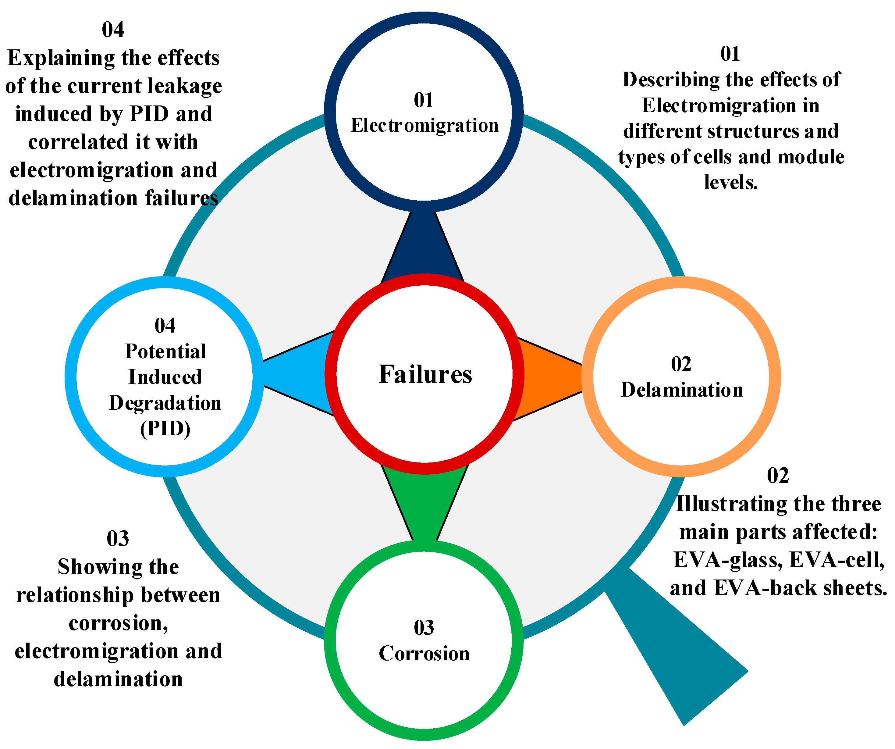
2. Summary of the Discussed Failure Modes

As a consequence of the installation’s geographical position, the degree to which the various degradation mechanisms impact the different PV technologies does not appear to be similar. It rather depends on the implemented technology, topology operations, and the cumulative background of exposure to meteorological conditions; subsequently, the rated PV power degrades at different levels. In this review, various sample tests conducted in different countries such as the United States, German, Mexico, South Korea, and Russia have been checked and presented. However, the results concluded from the experiments vary from one country to another even though they have the same exposure period. Figure 1 shows the typical failure modes discussed in this review.

3. Delamination Failures

3.1. ALTs for Delamination Failures

ALTs are stresses subjected to the PV module until the failure occurs, whereas specific durations of stresses are assigned in qualification certificate testing [43]. Some of the delamination failures can be easily observed on the PV modules operating in the field via visual inspection. Additionally, certain test procedures in the laboratory experience the same failures seen in the field. To improve the reliability of photovoltaic modules, multiple ATLs were developed on the industry side to predict the lifetime of the PV modules. ALTs are also used to mimic delamination failures. For instance, DH, whose parameters are 85 °C/85% RH for 1000 h, is required for IEC [44], humidity freeze, and UV exposure. However, some of the PV modules in the field that passed the IEC of DH test show a severe degradation rate [33]. Hence, some of the researchers change these parameters by increasing or decreasing to explore more about the failures. Table 1 is showing different ATLs with different parameters utilized to predict the delamination failure and the characterization tools.
Issa Faye et al. [44] investigated the consumer-type of minimodules where they were used in severe climate conditions in Senegal. Two modules were evaluated by the DH test for 1000 and 1300 h, respectively, using 85 °C and 85% RH. The other two modules (named C and D) were exposed to 55 and 66 cycles of thermal cycle (TC) test using a thermal chamber with diagnostic tools such as infrared (IR) thermal image, IV curve analysis, and electroluminescence (EL). The visual inspection confirmed that the modules were affected by corrosion, bubbles, and delamination. However, by observing the EL image of the modules C and D that had been through 66 and 55 cycles of TC, respectively, as shown in Figure 2, they summarized their findings:
  • Cells with a disrupted finger contact lead to darker areas in the solar cell’s active areas.
  • Dark spots in the cell region resulted from the solar cell cracks and/or metallization interruption: the 55-cycle minimodule displays five dark areas. The 66-cycle minimodule shows two dark region cells. The dark regions within the active region of a solar cell, as shown in Figure 2, suggest full disconnection, which may be triggered by the front or backside metallization interruptions.
  • Cells with discoloration provoked by corrosion undergo a rapid transition from dark to lighter regions.
Their overall result indicated that almost all defects found on the module were due to the impacts of exposure conditions. Consequently, the study’s findings suggest that the consumer-type c-Si minimodules may not be suitable for hot and humid African climates [44].

3.2. Encapsulation Delamination

The encapsulant used in Si modules is a polymeric substance, and it functions to grant an adhesion to the solar cell and the glass, the back sheet and solar cell, and any location within the back sheet and the glass. Moreover, it gives mechanical assistance to the module structure and cell configuration while providing enough optical binding, PV cell protection against electrical agents, and other external actions [49]. For approximately three decades, the materials utilized as encapsulants are the EVA copolymers and EVA materials encapsulated nearly 80% of PV modules. However, EVA is the most generally used investor in encapsulated Si-based PV modules [50,51].
Various studies have reported that encapsulant delamination was among the most significant common field failures for PV modules [52,53]. Figure 3 illustrates the structure of the c-Si PV module. Encapsulant is one of the essential materials of the PV module. Hence, it should be more reliable to optimize the module efficiency.
Meena et al. [55] examined the delaminated and discolored encapsulant degradation of 20-year-old c-Si solar panels. Findings show that the gray delaminated EVA deterioration is associated with the reflection effects at high wavelengths. By contrast, the absorption at low wavelengths is referred to as the brown discolor that appeared on the EVA. Their results indicated that the influence of these effects on panel output was observed as a loss in short-circuit current, with a further power loss due to cell failure. Furthermore, simulation for the degraded region’s effect showed a loss in the solar panel’s output power of more than 40%. All in all, they demonstrated the qualitative impacts of predominant EVA deterioration that are possibly beneficial for developing the EVA design and production for PV modules factories.
In Wohlgemuth et al. [56], during the visit for PV arrays, the National Renewable Energy Laboratory (NREL) community observed any changes in PV modules. Three different observations of delamination have been reported in this paper: encapsulant–glass delamination, encapsulant–cell delamination, and back-sheet delamination [56]. Remarkably, the encapsulant delamination is considered to be one of the main degradations that affect the PV modules’ overall performance. As discussed previously, various forms of encapsulant delamination were identified in the field, including front glass–encapsulant delamination, cells, interconnecting ribbons, and back sheet [57,58]. Conversely, they mostly share some of the effects, causes, and mechanisms, and they differ in impacting PV modules. For instance, the EVA–cell and EVA–glass delaminations are more damaging than the EVA–back-sheet delamination [45,59]. Table 2 illustrates the differences of these three types.
A similar observation has been demonstrated by N. C. Park et al. [59] during the failure analysis of a PV module. They confirmed that delamination happened at the EVA sheet and glass interfaces, following the EVA sheet and solar cell. Moreover, delamination exists at the back sheet, as shown in Figure 4 [59]. The electrical properties of the 25-year-old module located in Yeosu, South Korea, show a decreasing Pmax by 17.9%, ISC by 17.7%, and VOC by 1.9% from the initial measurement. The leading cause of this reduction was suggested to be the minimizing of transmittance light, which occurred because of the discoloration and delamination that directly affect the ISC.
Other mechanisms that help the occurrence of encapsulant delamination are chemical reactions that break the bond interface because of the humidity or material contamination and photothermal reaction that break the bond interface due to UV light and high temperature [43,56]. Lastly, the effects of the mentioned mechanisms could resemble a power drop beyond the warranty limit, promoting corrosion and moisture ingress to the structure of the PV module.

3.3. Delamination Associated with Corrosion

Li et al. [34] claimed that corrosion and delamination are cooperative and encourage mutual development between them. They observed the electrochemical reduction reaction of water with the metallization via dump heat test (1000 h, 85% RH, and 85 °C) followed by the biasing test (−1000 V, 292 h, 95% RH, and 72 °C) for a mini-PV module as shown in Figure 5 [34]. They confirmed that the degree of corrosion depends on the encapsulant resistance against the alkaline solution. It has also been reported that electrochemical reaction mechanisms in the PV modules drive the leakage current that primarily contributes to the occurrence of corrosion and delamination [34,61,62]. In this case, hydroxide ions and hydrogen gas are caused by the electrochemical reduction reactions of an ionic factor of the leakage current subjected to negative biasing. The hydrogen gas acts as a promoting agent for delamination when it accumulates on the metal surface, whereas hydroxide ions are altering the local environment near the metallization. Therefore, the corrosion of Si or SiO2 materials in solar cells within the alkaline environment destroys the bonds that exist between the encapsulant and the cell’s surface.
Figure 6a illustrates Ag fingers’ morphology analyzed using scanning electron microscopy (SEM) and associated energy-dispersive X-ray spectroscopy (EDS) mapping of the element at the selected area in Figure 5. Granular particles, such as Na, O, and Si, were found in the SEM images on the edge of Ag’s fingers that were not detected in the unexposed cell. The EDS analysis shows that the materials’ composition was 40.9 wt % Si, 44.1-wt % O, and 7.3-wt % Na and indicated that they were Si corrosion products [34]. These materials reacted with the hydroxide ions, leading to silicate creation, as shown in Figure 6b. It should be mentioned that the hydroxide ions are heavily concentrated close to metal fingers and enter through the pinhole in the nitride layer [63,64]. The OH ions, which create an alkaline environment, damages the bonds that exist between the encapsulant and solar cell and lead to the occurrence of delamination [34]. The electrochemical reactions could be written as:
Si + 6 OH SiO 3 2 + 3 H 2 O + 4 e
2 H 2 O + 2 e H 2 + 2 OH
resulting in,
Si + 2 OH + H 2 O 2 H 2 + SiO 3 2
and SiO 2 dissolves by the acid–base reaction
SiO 2 + 2   OH   H 2 O +   SiO 3 2
Asadpour et al. [65] conducted a one-dimensional simulation focusing on the delamination and corrosion of fingers on a c-Si solar cell/module’s front side. Since the layer’s thickness is only a few millimeters, which is negligible relative to the module area, a reasonable approximation of a three-dimensional structure would be a one-dimensional simulation, as shown in Figure 7. Reportedly, the reduction of Ag finger thickness via corrosion enhances the series resistance of the cell–module and reduces the efficiency [65].
The previous report has also shown that corrosion would not be a concern for Tampa, Florida, with a temperature mean of nearly 23 °C and 79% RH for well-built systems. However, a high percentage of module output deterioration if the environmental condition is 85 °C/85% RH tends to be a severe failure relative to the field conditions. Additionally, delamination often will not be a problem if the only trigger is the moisture penetration from the glass and the encapsulant.

3.4. Delamination Associated with PID

PID has become the subject of recent research [66]. According to the authors of the article, such delamination is accompanying PID, which occurred for different commercial c-Si PV modules that share common construction, particularly at the grid fingers region. Conversely, thin films, such as CdTe and Si photovoltaic modules, are affected by the PID, which occurred because of the delamination around the TCO layer [67]. Delamination is the leading cause of PID in TF Si PV modules [41]. A PV station’s output power loss can be up to 30% when severe PID affects it [68]. The PID mode of c-Si PV modules in the field was first introduced in 2010 [69] and especially for P-type PV modules that gained much attention [70]. Through the encapsulation and front glass, PID leads to high paths of leakage between the cells and the ground [71]. Early research investigations suggested that the onset of PID included the combined impacts of EVA encapsulation, soda lime front glass sheets, and the solar cell’s antireflective coating, which is a highly traditional mixture of the attributes of commercial PV modules. Exploring PV modules’ real world showed that the PID relies more on external parameters such as high voltage, temperature, and humidity [72,73]. Na ions from soda lime glass have been demonstrated to play a significant role in the degradation cycle [74,75].
By contrast, the use of borosilicate glass that consists of alkali metal of high K and low Na could improve the initial PV performance [76]. Additionally, microscopic analyses have shown the existence of sodium precipitates on solar cell surfaces. Observing the effect of PID could be accomplished by focusing on the mobile sodium ions and other metal ions through the microscopic image [77,78] and impedance spectroscopy [79]. However, PID was also confirmed in sodium-free glass specimens and suggested that the PID resulted from some ionic strain movement and is not directly linked to Na migration [71]. Table 3 shows a similar indoor test and field PID associated with the delamination failure of different Si PV modules.
For instance, Peter Hacke et al. [37] at the NREL conducted a test on four c-Si PV modules of 250 W. PID–delamination test conducted to the four modules on the basis of the sequence of 85 °C, 85%(RH), 1000 h DH test followed by a PID test of 72 °C, 95% RH, and −1000 V. This study shows that the delamination occurred after 156 h and again after 292 h of the PID test in module #3, at the same time the power loss was observed in the three modules together with the one experienced the delamination. However, module #4 showing neither power drop nor delamination had the lowest characteristic current transfer along the experiment course, whereas module #3 showing delamination had the highest current transfer. They conclude that the factors that lead to delamination are Na accumulation at the cell’s surface develop degrading adhesion, DH, and gaseous byproducts electrochemical motivated by the negative voltage supplied to the active cell circuit.
Naumann et al. [80] provided a precise observation of the PID mechanism. Their paper showed sodium’s prevalence in decorating preferentially the deep channels correlated with silicon stacking defects that were native to the process of multicrystalline solar cell crystallization [80]. Most of these stacking faults were deep enough to channel carriers directly through the emitter area and bypass the PN junction. The mechanistic reason for the reversible shunt resistance shift is the out diffusion of sodium from the stacking faults under the inverse bias process, as shown in Figure 8. The Na ion migrates via the glass, and EVA encapsulants accumulate on the cell surface and decorate Si bulk stacking faults [81].

4. EM Failure

EM failure is considered one of the degradation mechanism modes besides the corrosion failure in contact metallization and interconnects of PV systems. Degrading the contact layer increases the value of the series resistance, whereas EM failure can influence the series and shunt resistance [82]. Mainly EM failure has been widely investigated in the ICs, especially on the interconnect’s technology of ICs since the aluminum metal is used in interconnection films. EM is a diffusion mechanism that occurs when the interconnecting tracks’ current density is high enough to allow the metal atoms to migrate (diffusion) in the electron flow direction [19]. According to Michael G. Pecht’s book [19], two factors are responsible for the occurrence of EM: the environmental and material factors.
On the one hand, material factors such as the chemical composition may trigger the metallization system’s contact, e.g., Al, prone to EM. Next, a physical composition, the crystal grain size, e.g., the number of grain boundaries and void density in the metallization. Moreover, electron current is another environmental factor that causes Al ions to migrate [19]. EM in the metal electrode in solar cells could potentially occur with the same mechanism explained in [19].
J. Li et al. [83] used a buffer layer to establish an ohmic contact in the CdTe solar cells, where this buffer layer is used to reduce the barrier height. The author experimented with the Au, Ti, and Cr as a metallization layer along with ZnTe: Cu as a buffer layer. Experimental results show that the optimum thickness of the additive Cu to the metallization is, Au:15 nm, Ti:10 nm, and Cr:5 nm, where their efficiencies are 14.5%, 14.1%, and 14%, respectively. Hence, this a good indication for a successful back contact creation. Later on, these samples undergo an ALT in dark and light stressing under a temperature of 85 °C. Dark stressing shows a sharp decrease in efficiency at the initial hours. Then, it stabilized after 100 h at 80–85%. Conversely, under illumination stress, it experiences a huge decline at the first 5 h and stabilization when the t > 125 for all the metals where Ti had the highest efficiency of 86% compared with others where they stabilized at 64% for Cr and 49% for Au. Thus, they reveal that the severe degradation under the illumination was because of the EM of (Cu+) since the cells are biased at almost the VOC of the cell. However, this study did not consider environmental factors such as humidity, which we believe has a huge contribution to the EM [84]. Moreover, the combination of humidity, temperature, and voltage (HTV) can be found in aging tests, such as PID. The degradation of metallization within the c-Si PV modules and the corrosion of the TCO layer of TF PV modules are other types of PID effects [80], where ion migration is accelerated by these three combinations HTV [84]. Particularly, Ag fingers’ corrosion and the migration of ions from interconnect ribbon to the grounded frame of PV module, which mostly happens in areas that are experiencing high moisture ingress.

4.1. EM in Metal Film Interconnects

In general, because of the high temperature and sometimes the high current density that passes through the interconnects, they are prone to EM since they are made of metals such as aluminum, copper, and silver [85,86,87,88]. Interconnection technology plays a significant role in the reliability of PV modules since it is responsible for transporting the current from one cell to another. Therefore, any damage or extra stress among the interconnects could lead to a massive drop in the efficiency in both levels of cells and modules, especially for c-Si PV. The integrity of the solder interconnection impacts the power conversion efficiency and output power as well [89]. In solar cells, especially for organic cells, Khaligh and Goldthorpe [90] showed that in an unsatisfactory short time, the silver nanowire electrodes fail specifically and wires with high-level sheet resistance and electrodes that are subject to high-level current densities fail faster. They also examined the characteristics of EM and attempted to correlate it with the failure of wires. Therefore, the reason behind the electrode’s failure is that the silver nanowires are suffering from instability at higher temperatures provoked via Joule heating.
Certain challenges arise when using Cu metal as contacts in Si solar cells, especially as a front contact. Alison Lennon [91] identified three key challenges affecting the application of copper-plated Si PVs metallization, namely, (1) increase in carrier recombination due to the use of a copper metal for contact formation, (2) reliability issues due to failures of contact integrity or adhesion, and (3) shortage of cost-effective metal plating processes and equipment. Thus, for Si PV cell contacts, the technological benefits of utilizing Cu are not as convincing as using it for IC since PV cells could withstand relatively large feature sizes, thereby reducing the criticality of the contact’s conductivity and EM properties metal. Conversely, PV cells face another challenge, like the need to function in the field for more than 25 years in different climatic conditions [91].
Another challenge that could face the interconnects of silicon PVs is the soldering process. Zarmai et al. [92] conducted a review work for the current reliability challenges of interconnection technologies and identification of the suitable technique for the solar cell interconnection assembly. Their results indicate that the trending soldering technology of interconnection ribbon in silicon solar cells is the laser soldering since it produces a more reliable interconnection joint from the front to the back of the cell’s surface. However, it induces mechanical and thermal stresses in the cell and joints, which results in series resistance and shadowing losses in crystalline silicon solar cells. Therefore, they suggested conducting more R&D to reduce the losses of series resistance [92]. In light of that, the rear and top metal contacts and the ribbons are made of copper (Cu), silver (Ag), or aluminum (Al), which are prone to EM.
EM phenomena have been reported in c-Si solar cells [25,26]. Numerous solar cell degradations could be correlated with the edge of the cell, usually erratic such as CdTe thin films. Exposure of the diode’s front and back junctions at the corners and edges makes it more susceptible to environmental pressure and EM ending in a “very shunted, very leaky” microdiode, significantly affecting the efficiency of the other 99.95% of the cell [22]. Additionally, the most susceptible metal to migration is silver because the migration process required low activation energy [93]. Ag electroplating is used to reduce the contact finger’s electrical resistance. However, because of the toxic CN ions of Ag plating, there is a safety issue that arises, and another environmental issue shows up because of the detoxication of the plating. Therefore, Kang et al. [25] studied the idea of using Cu metallization instead of Ag metallization for Si solar cells since Cu has better EM resistance.
Colwell et al. [94] studied the reliability of copper-plated front side metallization of Si solar cells by exposing them to long-range thermal tests. The sun’s VOC measurements experience a noticeable voltage bend-back shown in Figure 9 during higher intensities of more than one sun illumination followed by 200 °C for a 500 h thermal stress of laser-ablated cells with a Ni/Cu/Ag plated front metal panel. Therefore, throughout the thermal annealing, the authors revealed that huge voids could develop within the Ag capping layer and the primary Cu stack, where the effects of the presence of voids in the grid line (Ag’s fingers) are increasing the series resistance and line resistance, which also reduce the FF [94,95].
Nonetheless, another observation was that new metal layer consisting largely of diffused Cu straight over the Ag capping, as shown in Figure 10b,d for both immersion Ag cell and light-induced plating (LIP) cell; also, in Figure 11, the EDS map is the clearer image with the presence of the new layer. It was hypothesized that the voids grow through the capping metal was because of the grain boundary diffusion. This theory is backed by earlier low-temperature Cu diffusion studies along dislocations and grain boundaries of polycrystalline metals such as Au [94]. The Schottky behavior’s origin was theoretically due to higher contact resistance from the voids that are assumed to form as a consequence of Cu’s grain boundary diffusion through the Ag capping layer. However, it has been shown that the voids could collapse by “scratching” the busbar with the measuring probe, after which Schottky behavior was no longer observed in Suns–VOC curve measurements [94].
For Cu EM, the formation of voids attributed to Cu diffusion has been observed [96]. Although Cu diffusion through the capping metal could pose questions regarding the plated module’s durability, it has been demonstrated that if the thermal test was implemented at a reduced temperature of 80 °C, then void formation can be prevented. Additionally, the grain boundary diffusion is motivated by the existence of the sinks. The encapsulant around the metal might remove the sink reactions presented in this cell experiment [94]. However, this study suggests investigating the possibility of Cu diffusion via the Ag capping layers in modules with encapsulation technology and the impact if it happened [94].
Dang et al. [97] conducted another reliability testing on the plated Ni/Cu/Ag metallization for c-Si solar cells. It was indicated that this structure could be a promising replacement for Ag metal contact because of its good resistivity for EM. According to their results during the cell processing, some of the nickel particles diffused in. Another observation was for the migration of copper to the silicon surface after aging at 235 °C; however, at the Ni/Si interface, there is less Cu separation when using soft-laser ablation compared with the hard-laser ablation method. Thereby, the diffusion of copper through the silver layer has led to the formation of CuOx on the Ag layer, creating massive voids at the interface of Cu/Ag as shown in Figure 12, because the specimens were brought out periodically for electrical measurement. Hence, the impacts of the Cu migration on the cell performance require further studies, particularly for the real-life operation [97].
Kuan-Jen Chen et al. [26] studied a module’s structure (Ag/solder/Cu·Zn/Al) with a hot dipping and an electroplated Sn PV ribbon that reflowed onto the Ag electrode on a silicon solar cell was tested to estimate its feasibility over the traditional (Ag/solder/Cu/Al) module. A bias-aging test evaluates the growth of intermetallic compounds (IMCs) promoted by the bias-induced thermal diffusion and EM. However, the Ag3Sn joined with the photovoltaic Al ribbon and the silicon solar substrate, whereas the Cu6Sn5 IMC grows at the Cu/Sn interface. Additionally, the hot-dipped PV module has a thicker Ag3Sn IMC at the Sn/Ag interface compared with the electroplated (EP) PV module, which would be correlated with a higher temperature return flow [26].
Additionally, compared with the previous results, EP and HD PV modules with Ag-direction biased had a higher growth mechanism of IMCs’ Cu6Sn5 and Ag3Sn because of EM’s driving force direction. Especially, Ag3Sn IMC overgrows following the biasing of the Ag direction, increasing the module’s series resistance. Improving the Al-ribbon conductivity and decreasing IMC’s overgrowth attitude in the EP PV module has led to reducing the module architecture’s series resistance, having the potential for solar cell applications [26].

4.2. Characteristics of EM

Mainly, voids and hillocks are the characteristics of EM phenomena [98]. In metallic wires, the wind force causes preliminary damage (voids) on the cathode side and hillocks on the anode side, whereas the direct force produces void on the anode side and hillocks on the cathode side [99]. Quan Sun and his team [100] studied the effect of stress migration and thermal fatigue of silver thin films on the flexible substrate. Their results indicated that the combination of thermal fatigue and stress migration increases the number of atomic diffusions then causes the thin films to experience cracks, voids, and hillocks, which could cause the electrical conductivity to deteriorate [100]. According to Liu et al. [101], copper diffuses into the silver layer’s vacancies after the annealing process, and then the vacancies transfer to the copper layer. Thereby, suppose the copper layer does not have sinks to absorb these vacancies. In this case, this will lead to the nucleation of voids at the copper/silver interface since the vacancies will be in supersaturated condition.
EM failure in rigidly passive metal interconnecting lines is analyzed with specific respect to vacancy supersaturations and hydrostatic stresses, which could be formed under EM circumstances while blocking grain boundaries [102]. It can be seen that the elevated stresses required for homogeneous void nucleation are likely too high for EM to create, and that breakdown is more likely to involve the growth of already presented voids. A study of the EM of the already existing small voids indicates that large voids migrate quicker than smaller voids above the critical size. This may lead to a disastrous mechanism where larger voids could catch up with smaller ones and coalesce with them, expand in size and move faster as they do so. Hence, Nix and Arzt assumed that the pre-existing voids migration and coalescence is possible for the mechanism of EM failure [102].
Several methods were introduced to study EM material diffusion because of the stress of the electrical current. In situ SEM EM inspections allow mass transport to be observed by examining the time-dependent development of voids and hillocks in metallic interconnections [103]. In Cu nanowires, Qiaojian Huang et al. [103] have extensively studied EM with a thickness of 50 nm and widths of 90 and 141 nm. The experiments in situ were carried out using the measurement of in situ resistance with SEM analysis. The mean time to fail approach was measured and used to calculate the activation energy. The activation energies for a nanowire width of 90 nm were 1.06 eV, whereas for a width of 141 nm, the activation energy was 0.94 eV. The findings support the author’s statement that surface diffusion can be a significant failure mechanism of nanoscale wires from EM.
Archana Sinha et al. [48] illustrated the deterioration mechanism and impact of the subsequent mass transport of Ag from the cell gridline into EVA in high positive voltage bias stressed minimodules. The results from their study show that the corrosion of silver gridlines causes discoloration and enables adhesion failure (delamination) at the EVA/cell interface. This was attributed to the +1000 V bias, which drives the degradation and not just the DH ALT 85 °C/85% RH or 75 °C/85% RH on the samples. According to the chemical analysis, they assumed that Ag reacts with any sulfur available at the interface and then reacts with oxygen, leading to both the sulfide and the oxide species being mixed, where the source of the sulfur was from the back sheet. This finding is opposite to the −1000 bias where sodium ions migrating from the cover glass to the solar cell are liable for the deterioration. The module deterioration under +1000 bias is driven by the silver ions migrating from the cell gridlines toward the glass. As a result of the positive bias degradation in this study, the power loss was in the range of 30–32%, which is predominantly due to loss of ISC.

5. Conclusions

Precise and efficient analysis of PV technology’s performance degradation is the next logical step in achieving PVs’ advantages, as modern, more effective innovations grow with poorly understood and unclear longevity and environment capability. To better understand the deterioration of PV’s performance, there should be more insightful analyses and investigations for different levels, cells, modules, and systems to find the dominant factors behind PVs’ failures. Therefore, this review illustrated numerous studies that have been done for both delamination and EM in different PV types, levels, and provided mechanisms correlation with other failures such as corrosion and PID. Moreover, the paper shows the characteristics of EM in different electrode metals such as silver, copper, and aluminum, where they are used as front and rear contact metals and interconnects of the solar cells. Overall causes are high temperature, high moisture, and high leakage current, which also impact the organic materials such as EVA and lead them to delaminate, particularly at the fingers’ area where the generated heat may be because of the EM occurrence. Although accelerated tests prove their ability to reproduce the delamination, corrosion, and PID, EM is an open topic, and the criteria to distinguish it remain unclear in the PV technologies. Some studies show promising results for improving the PV’s performance and reliability, whereas others failed to do this, especially for EM failure. Additionally, since the metallization is improving in PV modules especially for front contacts (by reducing the thickness of fingers), EM failure should be considered. We believe that there is a strong correlation between delamination and EM. Hence, from our in-depth analysis insights of the IC technology, we suggested recommendations that should be considered for metal contact and interconnect investigations in PV technology. Future investigations should be applied to find an ideal module component as an alternative to traditional materials such as EVA used as an encapsulation material and ideal electrode and busbar materials in solar cells that can resist delamination and EM.

Author Contributions

Conceptualization, A.A.A. and N.A.; methodology, A.A.A. and N.A.; validation, M.A.I., A.A.A. and N.A.; formal analysis, S.A.S. and M.A.I.; investigation, A.A.Q.H.; resources, A.A.Q.H.; data curation, A.A.Q.H.; writing—original draft preparation, A.A.Q.H.; writing—review and editing, A.A.A., S.A.S., M.A.I. and M.N.E.A.; visualization, A.A.Q.H.; supervision, A.A.A. and N.A.; project administration, A.A.A.; funding acquisition, A.A.A. All authors have read and agreed to the published version of the manuscript.

Funding

This research is financially supported by the grant code of FRGS/1/2019/TK07/UNITEN/02/7 from the Ministry of Higher Education (MoHE) of Malaysia.

Data Availability Statement

Not applicable.

Acknowledgments

The authors wish to thank the Ministry of Higher Education of Malaysia (MoHE) for providing the research grant with the code of FRGS/1/2019/TK07/UNITEN/02/7 to support this research. Authors also acknowledge the publication support through J510050002—BOLDREFRESH2025—CENTRE OF EXCELLENCE from the iRMC of Universiti Tenaga Nasional (UNITEN).

Conflicts of Interest

The authors declare no conflict of interest.

Abbreviations

AbbreviationDefinition
PVPhotovoltaic
PIDPotential-Induced degradation
IECInternational Electrotechnical Commission
c-SiCrystalline silicon
TFThin film
DHDamp heat
UVUltraviolet
ALTsAccelerated lifetime tests
RHRelative humidity
EMElectromigration
VocOpen-circuit voltage
FFFill factor
JscShort-circuit current density
ICIntegrated circuit
SiSilicon
EVAEthylene-vinyl acetate
RsSeries resistance
PmaxMaximum power
NaSodium
TCOTransparent conductive oxide
TCThermal cycle
IRInfrared
ELElectroluminescence
NRELNational Renewable Energy Laboratory
SEMScanning electron microscopy
EDSEnergy-dispersive X-ray spectroscopy
CdTeCadmium telluride
KPotassium
AlAluminum
AuGold
TiTitanium
CrChromium
CuCopper
AgSilver
PVEPolyvinyl fluoride
PETPolyethylene terephthalate
HTVHumidity, temperature, and voltage
LIPLight-induced plating
TEMTransmission electron microscopy
EPElectroplated
HDHot dipping
IMCsIntermetallic compounds
CTECoefficient of thermal expansion

References

  1. Khan, R.; Go, Y. Assessment of Malaysia’s Large-Scale Solar Projects: Power System Analysis for Solar PV Grid Integration. Glob. Chall. 2019, 4, 1900060. [Google Scholar] [CrossRef] [PubMed] [Green Version]
  2. Phinikarides, A.; Kindyni, N.; Makrides, G.; Georghiou, G.E. Review of photovoltaic degradation rate methodologies. Renew. Sustain. Energy Rev. 2014, 40, 143–152. [Google Scholar] [CrossRef]
  3. Singla, A.; Singh, K.; Yadav, V.K. Environmental effects on performance of solar photovoltaic module. In Proceedings of the 2016 Biennial International Conference on Power and Energy Systems: Towards Sustainable Energy (PESTSE), Bengaluru, India, 21–23 January 2016; pp. 1–6. [Google Scholar]
  4. Rahman, M.; Hasanuzzaman, M.; Rahim, N. Effects of various parameters on PV-module power and efficiency. Energy Convers. Manag. 2015, 103, 348–358. [Google Scholar] [CrossRef]
  5. Meyer, S.; Timmel, S.; Gläser, M.; Braun, U.; Wachtendorf, V.; Hagendorf, C. Polymer foil additives trigger the formation of snail trails in photovoltaic modules. Sol. Energy Mater. Sol. Cells 2014, 130, 64–70. [Google Scholar] [CrossRef]
  6. Peng, P.; Hu, A.; Zheng, W.; Su, P.; He, D.; Oakes, K.D.; Fu, A.; Han, R.; Lee, S.L.; Tang, J.; et al. Microscopy study of snail trail phenomenon on photovoltaic modules. RSC Adv. 2012, 2, 11359–11365. [Google Scholar] [CrossRef]
  7. Pozza, A.; Sample, T. Crystalline silicon PV module degradation after 20 years of field exposure studied by electrical tests, electroluminescence, and LBIC. Prog. Photovolt. Res. Appl. 2015, 24, 368–378. [Google Scholar] [CrossRef] [Green Version]
  8. Ndiaye, A.; Kébé, C.M.; Charki, A.; Sambou, V.; Ndiaye, P.A. Photovoltaic Platform for Investigating PV Module Degradation. Energy Procedia 2015, 74, 1370–1380. [Google Scholar] [CrossRef] [Green Version]
  9. Ishii, T.; Masuda, A. Annual degradation rates of recent crystalline silicon photovoltaic modules. Prog. Photovolt. Res. Appl. 2017, 25, 953–967. [Google Scholar] [CrossRef]
  10. Omazic, A.; Oreski, G.; Halwachs, M.; Eder, G.; Hirschl, C.; Neumaier, L.; Pinter, G.; Erceg, M. Relation between degradation of polymeric components in crystalline silicon PV module and climatic conditions: A literature review. Sol. Energy Mater. Sol. Cells 2019, 192, 123–133. [Google Scholar] [CrossRef]
  11. Köntges, M.; Kurtz, S.; Packard, C.E.; Jahn, U.; Berger, K.; Kato, K.; Friesen, T.; Liu, H.; Van Iseghem, M. Review of Failures of Photovoltaic Modules: IEA PVPS. Available online: https://repository.supsi.ch/9645/ (accessed on 21 March 2021).
  12. Bouaichi, A.; Merrouni, A.A.; Hajjaj, C.; Messaoudi, C.; Ghennioui, A.; Benlarabi, A.; Ikken, B.; El Amrani, A.; Zitouni, H. In-situ evaluation of the early PV module degradation of various technologies under harsh climatic conditions: The case of Morocco. Renew. Energy 2019, 143, 1500–1518. [Google Scholar] [CrossRef]
  13. Gambogi, W.; Fu, O.; Bradley, A.; Stika, K.; Hamzavy, B.; Smith, R.; Sample, T. The impact of materials properties on PV module performance and durability. In Proceedings of the 27th European Photovoltaic Solar Energy Conference and Exhibition, Frankfurt, Germany, 24–28 September 2012. [Google Scholar]
  14. Kuitche, J.; TamizhMani, G. Accelerated Lifetime Testing of Photovoltaic Modules Solar America Board for Codes and Standards; A Report of Solar America Board for Codes and Standards; 2013; Available online: http://www.solarabcs.org/about/publications/reports/acceleratedtesting/pdfs/SolarABCs-33-2013.pdf (accessed on 28 March 2021).
  15. Xia, Z.; Wohlgemuth, J.H.; Cunningham, D.W. A lifetime prediction of PV encapsulant and backsheet via time temperature superposition principle. In Proceedings of the 2009 34th IEEE Photovoltaic Specialists Conference (PVSC), Philadelphia, PA, USA, 7–12 June 2009; pp. 000523–000526. [Google Scholar]
  16. Dong, N.C.; Islam, M.A.; Ishikawa, Y.; Uraoka, Y. The influence of sodium ions decorated micro-cracks on the evolution of potential induced degradation in p-type crystalline silicon solar cells. Sol. Energy 2018, 174, 1–6. [Google Scholar] [CrossRef]
  17. Sharma, V.; Chandel, S. Performance and degradation analysis for long term reliability of solar photovoltaic systems: A review. Renew. Sustain. Energy Rev. 2013, 27, 753–767. [Google Scholar] [CrossRef]
  18. Kumar, S.; Meena, R.; Gupta, R. Imaging and micro-structural characterization of moisture induced degradation in crystalline silicon photovoltaic modules. Sol. Energy 2019, 194, 903–912. [Google Scholar] [CrossRef]
  19. Jevtic, M. Guidebook for Managing Silicon Chip Reliability; Michael, G.P., Riko, R., Gopal, R., Eds.; CRC Press: Boca Raton, FL, USA, 1999; 224p, ISBN 0-8493-9624-7. [Google Scholar]
  20. Balaji, N.; Raval, M.C.; Saravanan, S. Review on Metallization in Crystalline Silicon Solar Cells. Solar Cells 2020. [Google Scholar] [CrossRef] [Green Version]
  21. Dullweber, T.; Stöhr, M.; Kruse, C.; Haase, F.; Rudolph, M.; Beier, B.; Jäger, P.; Mertens, V.; Peibst, R.; Brendel, R. Evolutionary PERC+ solar cell efficiency projection towards 24% evaluating shadow-mask-deposited poly-Si fingers below the Ag front contact as next improvement step. Sol. Energy Mater. Sol. Cells 2020, 212, 110586. [Google Scholar] [CrossRef]
  22. McMahon, T.J.; Berniard, T.J.; Albin, D.S. Nonlinear shunt paths in thin-film CdTe solar cells. J. Appl. Phys. 2005, 97, 054503. [Google Scholar] [CrossRef]
  23. Lloyd, J. Black’s law revisited—Nucleation and growth in electromigration failure. Microelectron. Reliab. 2007, 47, 1468–1472. [Google Scholar] [CrossRef]
  24. Heimann, M.; Klaerner, P.; Luechinger, C.; Mette, A.; Mueller, J.; Traeger, M.; Barthel, T.; Valentin, O.; Wawer, P. Ultrasonic Bonding of Aluminum Ribbons to Interconnect High-Efficiency Crystalline-Silicon Solar Cells. Energy Procedia 2012, 27, 670–675. [Google Scholar] [CrossRef] [Green Version]
  25. Kang, J.; You, J.; Kang, C.; Pak, J.J.; Kim, D. Investigation of Cu metallization for Si solar cells. Sol. Energy Mater. Sol. Cells 2002, 74, 91–96. [Google Scholar] [CrossRef]
  26. Chen, K.-J.; Hung, F.-Y.; Lui, T.-S.; Lin, W.-Y. Effects of Static Heat and Dynamic Current on Al/Zn∙Cu/Sn Solder/Ag Interfaces of Sn Photovoltaic Al-Ribbon Modules. Materials 2018, 11, 1642. [Google Scholar] [CrossRef] [PubMed] [Green Version]
  27. Urrejola, E.; Peter, K.; Plagwitz, H.; Schubert, G. Silicon diffusion in aluminum for rear passivated solar cells. Appl. Phys. Lett. 2011, 98, 153508. [Google Scholar] [CrossRef] [Green Version]
  28. Urban, T.; Mette, A.; Heitmann, J. Influence of Silver-Aluminium Alloy at Solar Cell Rear Side on Series Resistance and Open Circuit Voltage. Energy Procedia 2016, 92, 236–241. [Google Scholar] [CrossRef] [Green Version]
  29. Zhang, J.; Gao, X.; Deng, Y.; Zha, Y.; Yuan, C. Comparison of life cycle environmental impacts of different perovskite solar cell systems. Sol. Energy Mater. Sol. Cells 2017, 166, 9–17. [Google Scholar] [CrossRef]
  30. Chattopadhyay, S.; Dubey, R.; Kuthanazhi, V.; John, J.J.; Solanki, C.S.; Kottantharayil, A.; Arora, B.M.; Narasimhan, K.L.; Kuber, V.; Vasi, J.; et al. Visual Degradation in Field-Aged Crystalline Silicon PV Modules in India and Correlation with Electrical Degradation. IEEE J. Photovolt. 2014, 4, 1470–1476. [Google Scholar] [CrossRef]
  31. Kleiss, G.; Kirchner, J.; Reichart, K. Quality and Reliability-sometimes the customer wants more. In Proceedings of the NREL Photovoltaic Reliability Workshop, Golden, CO, USA, 24–27 February 2015. [Google Scholar]
  32. Bouraiou, A.; Hamouda, M.; Chaker, A.; Necaibia, A.; Mostefaoui, M.; Boutasseta, N.; Ziane, A.; Dabou, R.; Sahouane, N.; Lachtar, S. Experimental investigation of observed defects in crystalline silicon PV modules under outdoor hot dry climatic conditions in Algeria. Sol. Energy 2018, 159, 475–487. [Google Scholar] [CrossRef]
  33. Li, H.; Lv, F.; Diao, H.; Chen, X.; Wang, W. Evaluation of temperature and humidity on PV module degradation- in field degradation analysis of crystalline silicon module. In Proceedings of the 2019 IEEE 46th Photovoltaic Specialists Conference (PVSC), Chicago, IL, USA, 16–21 June 2019; pp. 1986–1990. [Google Scholar]
  34. Li, J.; Shen, Y.-C.; Hacke, P.; Kempe, M. Electrochemical mechanisms of leakage-current-enhanced delamination and corrosion in Si photovoltaic modules. Sol. Energy Mater. Sol. Cells 2018, 188, 273–279. [Google Scholar] [CrossRef]
  35. Sangpongsanont, Y.; Chenvidhya, D.; Chuangchote, S.; Kirtikara, K. Corrosion growth of solar cells in modules after 15 years of operation. Sol. Energy 2020, 205, 409–431. [Google Scholar] [CrossRef]
  36. Xiong, H.; Gan, C.; Yang, X.; Hu, Z.; Niu, H.; Li, J.; Si, J.; Xing, P.; Luo, X. Corrosion behavior of crystalline silicon solar cells. Microelectron. Reliab. 2017, 70, 49–58. [Google Scholar] [CrossRef]
  37. Hacke, P.L.; Kempe, M.D.; Wohlgemuth, J.; Li, J.; Shen, Y.C. Potential-induced degradation-delamination mode in crystalline silicon modules. In Proceedings of the 2016 Workshop on Crystalline Silicon Solar Cells and Modules: Materials and Processes, Vail, CO, USA, 28–31 August 2016. [Google Scholar]
  38. Spataru, S.V.; Sera, D.; Hacke, P.; Kerekes, T.; Teodorescu, R. Fault identification in crystalline silicon PV modules by complementary analysis of the light and dark current-voltage characteristics. Prog. Photovolt. Res. Appl. 2015, 24, 517–532. [Google Scholar] [CrossRef]
  39. Islam, M.A.; Oshima, T.; Kobayashi, D.; Matsuzaki, H.; Nakahama, H.; Ishikawa, Y. Carrier dynamics in the potential-induced degradation in single-crystalline silicon photovoltaic modules. Jpn. J. Appl. Phys. 2018, 57, 08RG14. [Google Scholar] [CrossRef]
  40. Del Cueto, J.A.; Rummel, S.R. Degradation of photovoltaic modules under high voltage stress in the field. In Proceedings of the Reliability of Photovoltaic Cells, Modules, Components, and Systems III, San Diego, CA, USA, 19 August 2010; Volume 7773. [Google Scholar] [CrossRef] [Green Version]
  41. Masuda, A.; Hara, Y. Potential-induced degradation of thin-film Si photovoltaic modules. Jpn. J. Appl. Phys. 2017, 56, 04CS04. [Google Scholar] [CrossRef] [Green Version]
  42. Cotfas, D.T.; Cotfas, P.A.; Floroian, D.I.; Floroian, L. Accelerated Life Test for Photovoltaic Cells Using Concentrated Light. Int. J. Photoenergy 2016, 2016, 1–7. [Google Scholar] [CrossRef] [Green Version]
  43. Ndiaye, A.; Charki, A.; Kobi, A.; Kébé, C.M.; Ndiaye, P.A.; Sambou, V. Degradations of silicon photovoltaic modules: A literature review. Sol. Energy 2013, 96, 140–151. [Google Scholar] [CrossRef]
  44. Faye, I.; Ndiaye, A.; Gecke, R.; Blieske, U.; Kobor, D.; Camara, M. Experimental study of observed defects in mini-modules based on crystalline silicone solar cell under damp heat and thermal cycle testing. Sol. Energy 2019, 191, 161–166. [Google Scholar] [CrossRef]
  45. Tracy, J.; Bosco, N.; Dauskardt, R. Encapsulant Adhesion to Surface Metallization on Photovoltaic Cells. IEEE J. Photovolt. 2017, 7, 1635–1639. [Google Scholar] [CrossRef]
  46. Shi, W.; Theelen, M.; Gevaerts, V.; Illiberi, A.; Barreau, N.; Butterling, M.; Schut, H.; Egger, W.; Dickmann, M.; Hugenschmidt, C.; et al. Positron Annihilation Studies on the Damp Heat Degradation of ZnO:Al Transparent Conductive Oxide Layers for CIGS Solar Cells. IEEE J. Photovolt. 2018, 8, 1847–1851. [Google Scholar] [CrossRef]
  47. Martin, I.; Oyster, T.M.; Mansfield, L.M.; Matthews, R.; Pentzer, E.B.; French, R.H.; Peshek, T.J. Interfacial modifiers for enhanced stability and reduced degradation of Cu(In, Ga)Se2 devices. In Proceedings of the 2016 IEEE 43rd Photovoltaic Specialists Conference (PVSC), Philadelphia, PA, USA, 7–12 June 2016; pp. 1489–1493. [Google Scholar]
  48. Sinha, A.; Moffitt, S.L.; Hurst, K.; Kempe, M.; Han, K.; Shen, Y.-C.; Miller, D.C.; Hacke, P.; Schelhas, L.T. Understanding interfacial chemistry of positive bias high-voltage degradation in photovoltaic modules. Sol. Energy Mater. Sol. Cells 2021, 223, 110959. [Google Scholar] [CrossRef]
  49. López-Escalante, M.; Caballero, L.J.; Martín, F.; Gabás, M.; Cuevas, A.; Ramos-Barrado, J. Polyolefin as PID-resistant encapsulant material in PV modules. Sol. Energy Mater. Sol. Cells 2016, 144, 691–699. [Google Scholar] [CrossRef]
  50. Peike, C.; Purschke, L.; Weiss, K.-A.; Kohl, M.; Kempe, M.D. Towards the origin of photochemical EVA discoloration. In Proceedings of the 2013 IEEE 39th Photovoltaic Specialists Conference (PVSC), Tampa, FL, USA, 16–21 June 2013; pp. 1579–1584. [Google Scholar]
  51. Jiang, S.; Wang, K.; Zhang, H.; Ding, Y.; Yu, Q. Encapsulation of PV Modules Using Ethylene Vinyl Acetate Copolymer as the Encapsulant. Macromol. React. Eng. 2015, 9, 522–529. [Google Scholar] [CrossRef]
  52. Tamizmani, G. Reliability Evaluation of PV Power Plants Input Data for Warranty, Bankability and Energy Estimation Models. In Proceedings of the PV Module Reliability Workshop 2014, Golden, CO, USA, 25 February 2014. [Google Scholar]
  53. Jordan, D.C.; Wohlgemuth, J.H.; Kurtz, S.R. Technology and Climate Trends in PV Module Degradation; National Renewable Energy Lab. (NREL): Golden, CO, USA, 2012.
  54. Farrell, C.; Osman, A.; Doherty, R.; Saad, M.; Zhang, X.; Murphy, A.; Harrison, J.; Vennard, A.; Kumaravel, V.; Al-Muhtaseb, A.; et al. Technical challenges and opportunities in realising a circular economy for waste photovoltaic modules. Renew. Sustain. Energy Rev. 2020, 128, 109911. [Google Scholar] [CrossRef]
  55. Meena, R.; Kumar, S.; Gupta, R. Comparative investigation and analysis of delaminated and discolored encapsulant degradation in crystalline silicon photovoltaic modules. Sol. Energy 2020, 203, 114–122. [Google Scholar] [CrossRef]
  56. Wohlgemuth, J.H.; Hacke, P.; Bosco, N.; Miller, D.C.; Kempe, M.D.; Kurtz, S.R. Assessing the causes of encapsulant delamination in PV modules. In Proceedings of the 2016 IEEE 43rd Photovoltaic Specialists Conference (PVSC), Portland, OR, USA, 5–10 June 2016; pp. 248–254. [Google Scholar]
  57. de Oliveira, M.C.C.; Cardoso, A.S.A.D.; Viana, M.M.; Lins, V.D.F.C. The causes and effects of degradation of encapsulant ethylene vinyl acetate copolymer (EVA) in crystalline silicon photovoltaic modules: A review. Renew. Sustain. Energy Rev. 2018, 81, 2299–2317. [Google Scholar] [CrossRef]
  58. Wohlgemuth, J.; Silverman, T.; Miller, D.C.; McNutt, P.; Kempe, M.; Deceglie, M. Evaluation of PV module field performance. In Proceedings of the 2015 IEEE 42nd Photovoltaic Specialist Conference (PVSC), New Orleans, LA, USA, 14–19 June 2015; pp. 1–7. [Google Scholar]
  59. Park, N.; Jeong, J.; Kang, B.; Kim, D. The effect of encapsulant discoloration and delamination on the electrical characteristics of photovoltaic module. Microelectron. Reliab. 2013, 53, 1818–1822. [Google Scholar] [CrossRef]
  60. Oh, W.; Bae, S.; Kim, S.; Park, N.; Chan, S.-I.; Choi, H.; Hwang, H.; Kim, D. Analysis of degradation in 25-year-old field-aged crystalline silicon solar cells. Microelectron. Reliab. 2019, 100–101, 113392. [Google Scholar] [CrossRef]
  61. Osterwald, C.; McMahon, T.; del Cueto, J. Electrochemical corrosion of SnO2:F transparent conducting layers in thin-film photovoltaic modules. Sol. Energy Mater. Sol. Cells 2003, 79, 21–33. [Google Scholar] [CrossRef]
  62. Asadpour, R.; Sun, X.; Alam, M.A. Electrical Signatures of Corrosion and Solder Bond Failure in c-Si Solar Cells and Modules. IEEE J. Photovolt. 2019, 9, 759–767. [Google Scholar] [CrossRef]
  63. Mon, G.R.; Ross, R.G., Jr. Amorphous-silicon module intercell corrosion. AIP Conf. Proc. 1987, 157, 350–357. [Google Scholar]
  64. Yen, B.K.; White, R.L.; Waltman, R.J.; Dai, Q.; Miller, D.C.; Kellock, A.J.; Marchon, B.; Kasai, P.H.; Toney, M.F.; York, B.R.; et al. Microstructure and properties of ultrathin amorphous silicon nitride protective coating. J. Vac. Sci. Technol. A 2003, 21, 1895–1904. [Google Scholar] [CrossRef] [Green Version]
  65. Asadpour, R.; Chavali, R.V.K.; Alam, M.A. Physics-Based computational modeling of moisture ingress in solar modules: Location-specific corrosion and delamination. In Proceedings of the 2016 IEEE 43rd Photovoltaic Specialists Conference (PVSC), Portland, OR, USA, 5–10 June 2016; pp. 840–843. [Google Scholar]
  66. Kaden, T.; Lammers, K.; Möller, H.J. Power loss prognosis from thermographic images of PID affected silicon solar modules. Sol. Energy Mater. Sol. Cells 2015, 142, 24–28. [Google Scholar] [CrossRef]
  67. Masuda, A.; Hara, Y.; Shiina, Y.; Okamoto, S.; Okamoto, T. Similarity of potential-induced degradation in superstrate-type thin-film CdTe and Si photovoltaic modules. Jpn. J. Appl. Phys. 2019, 58, SBBF07. [Google Scholar] [CrossRef]
  68. Jiang, F.; Liu, H.; Zou, X. Test and Analysis of Potential Induced Degradation in Crystalline Silicon PV Modules. In Proceedings of the 2018 Chinese Control and Decision Conference (CCDC), Shenyang, China, 9–11 June 2018; pp. 4993–4996. [Google Scholar]
  69. Oh, W.; Bae, S.; Chan, S.-I.; Lee, H.-S.; Kim, D.; Park, N. Field degradation prediction of potential induced degradation of the crystalline silicon photovoltaic modules based on accelerated test and climatic data. Microelectron. Reliab. 2017, 76–77, 596–600. [Google Scholar] [CrossRef]
  70. Oh, W.; Bae, S.; Kim, D.; Park, N. Initial detection of potential-induced degradation using dark I–V characteristics of crystalline silicon photovoltaic modules in the outdoors. Microelectron. Reliab. 2018, 88–90, 998–1002. [Google Scholar] [CrossRef]
  71. Pingel, S.; Frank, O.; Winkler, M.; Daryan, S.; Geipel, T.; Hoehne, H.; Berghold, J. Potential Induced Degradation of solar cells and panels. In Proceedings of the 2010 35th IEEE Photovoltaic Specialists Conference, Honolulu, HI, USA, 20–25 June 2010; Institute of Electrical and Electronics Engineers (IEEE); pp. 002817–002822. [Google Scholar]
  72. Ebneali, F.; Tatapudi, S.; Tamizhmani, G. Potential induced degradation of pre-stressed photovoltaic modules: Influence of polarity, surface conductivity and temperature. In Proceedings of the 2013 IEEE 39th Photovoltaic Specialists Conference (PVSC), Tampa, FL, USA, 16–21 June 2013; pp. 1548–1553. [Google Scholar]
  73. Hoffmann, S.; Koehl, M. Effect of humidity and temperature on the potential-induced degradation. Prog. Photovolt. Res. Appl. 2012, 22, 173–179. [Google Scholar] [CrossRef]
  74. Naumann, V.; Geppert, T.; Großer, S.; Wichmann, D.; Krokoszinski, H.-J.; Werner, M.; Hagendorf, C. Potential-induced Degradation at Interdigitated Back Contact Solar Cells. Energy Procedia 2014, 55, 498–503. [Google Scholar] [CrossRef]
  75. Oh, W.; Kim, J.; Kang, B.; Bae, S.; Lee, K.D.; Lee, H.-S.; Kim, D.; Chan, S.-I. Evaluation of potential-induced degradation in crystalline Si solar cells using Na fault injection. Microelectron. Reliab. 2016, 64, 646–649. [Google Scholar] [CrossRef]
  76. Muzzillo, C.P.; Glynn, S.; Hacke, P.; Moutinho, H.R.; Young, M.R.; Teeter, G.; Repins, I.L.; Mansfield, L.M. Potential-Induced Degradation of Cu(In,Ga)Se2 Solar Cells: Alkali Metal Drift and Diffusion Effects. IEEE J. Photovolt. 2018, 8, 1337–1342. [Google Scholar] [CrossRef]
  77. Naumann, V.; Lausch, D.; Graff, A.; Werner, M.; Swatek, S.; Bauer, J.; Hähnel, A.; Breitenstein, O.; Großer, S.; Bagdahn, J.; et al. The role of stacking faults for the formation of shunts during potential-induced degradation of crystalline Si solar cells. Phys. Status Solidi (RRL) Rapid Res. Lett. 2013, 7, 315–318. [Google Scholar] [CrossRef]
  78. Bauer, J.; Naumann, V.; Großer, S.; Hagendorf, C.; Schütze, M.; Breitenstein, O. On the mechanism of potential-induced degradation in crystalline silicon solar cells. Phys. Status Solidi (RRL) Rapid Res. Lett. 2012, 6, 331–333. [Google Scholar] [CrossRef]
  79. Katayama, N.; Osawa, S.; Matsumoto, S.; Nakano, T.; Sugiyama, M. Degradation and fault diagnosis of photovoltaic cells using impedance spectroscopy. Sol. Energy Mater. Sol. Cells 2019, 194, 130–136. [Google Scholar] [CrossRef]
  80. Naumann, V.; Lausch, D.; Hähnel, A.; Bauer, J.; Breitenstein, O.; Graff, A.; Werner, M.; Swatek, S.; Großer, S.; Bagdahn, J.; et al. Explanation of potential-induced degradation of the shunting type by Na decoration of stacking faults in Si solar cells. Sol. Energy Mater. Sol. Cells 2014, 120, 383–389. [Google Scholar] [CrossRef]
  81. Peshek, T.J.; Fada, J.S.; Martin, I. Degradation Processes in Photovoltaic Cells. In Durability and Reliability of Polymers and Other Materials in Photovoltaic Modules; Elsevier BV: Amsterdam, The Netherlands, 2019; pp. 97–118. [Google Scholar]
  82. Kumar, M.; Kumar, A. Performance assessment and degradation analysis of solar photovoltaic technologies: A review. Renew. Sustain. Energy Rev. 2017, 78, 554–587. [Google Scholar] [CrossRef]
  83. Li, J.; Ohno, T.R.; Wolden, C.A. The impact of different metallization layers on CdTe solar cells contacted with ZnTe:Cu buffer layers. In Proceedings of the 2016 IEEE 43rd Photovoltaic Specialists Conference (PVSC), Portland, OR, USA, 5–10 June 2016; pp. 1474–1479. [Google Scholar]
  84. Hacke, P.; Kempe, M.; Terwilliger, K.; Glick, S.; Call, N.; Johnston, S.; Kurtz, S.; Bennett, I.; Kloos, M. Characterization of Multicrystalline Silicon Modules with System Bias Voltage Applied in Damp Heat. In Proceedings of the 25th European Photovoltaic Solar Energy Conference and Exhibition/5th World Conference on Photovoltaic Energy Conversion, Valencia, Spain, 6–10 September 2010; pp. 3760–3765. [Google Scholar] [CrossRef]
  85. de Orio, R.; Ceric, H.; Selberherr, S. Physically based models of electromigration: From Black’s equation to modern TCAD models. Microelectron. Reliab. 2010, 50, 775–789. [Google Scholar] [CrossRef]
  86. Vanstreels, K.; Czarnecki, P.; Kirimura, T.; Siew, Y.K.; De Wolf, I.; Bömmels, J.; Tőkei, Z.; Croes, K. In-situ scanning electron microscope observation of electromigration-induced void growth in 30 nm ½ pitch Cu interconnect structures. J. Appl. Phys. 2014, 115, 74305. [Google Scholar] [CrossRef]
  87. Ceric, H.; Selberherr, S. Electromigration in submicron interconnect features of integrated circuits. Mater. Sci. Eng. R: Rep. 2011, 71, 53–86. [Google Scholar] [CrossRef]
  88. Theelen, M.; Daume, F. Stability of Cu(In,Ga)Se 2 solar cells: A literature review. Sol. Energy 2016, 133, 586–627. [Google Scholar] [CrossRef]
  89. Nyarko, F.K.; Takyi, G.; Amalu, E.H. Robust crystalline silicon photovoltaic module (c-Si PVM) for the tropical climate: Future facing the technology. Sci. Afr. 2020, 8, e00359. [Google Scholar] [CrossRef]
  90. Khaligh, H.H.; Goldthorpe, I.A. Failure of silver nanowire transparent electrodes under current flow. Nanoscale Res. Lett. 2013, 8, 235. [Google Scholar] [CrossRef] [Green Version]
  91. Lennon, A.; Colwell, J.; Rodbell, K.P. Challenges facing copper-plated metallisation for silicon photovoltaics: Insights from integrated circuit technology development. Prog. Photovolt. Res. Appl. 2019, 27, 67–97. [Google Scholar] [CrossRef] [Green Version]
  92. Zarmai, M.T.; Ekere, P.N.N.; Oduoza, C.; Amalu, E.H. A review of interconnection technologies for improved crystalline silicon solar cell photovoltaic module assembly. Appl. Energy 2015, 154, 173–182. [Google Scholar] [CrossRef]
  93. Berhe, T.A.; Su, W.-N.; Chen, C.-H.; Pan, C.-J.; Cheng, J.-H.; Chen, H.-M.; Tsai, M.-C.; Chen, L.-Y.; Dubale, A.A.; Hwang, B.-J. Organometal halide perovskite solar cells: Degradation and stability. Energy Environ. Sci. 2016, 9, 323–356. [Google Scholar] [CrossRef]
  94. Colwell, J.; Hsiao, P.-C.; Shen, X.; Zhang, W.; Wang, X.; Lim, S.; Lennon, A. Impact of contact integrity during thermal stress testing on degradation analysis of copper-plated silicon solar cells. Sol. Energy Mater. Sol. Cells 2018, 174, 225–232. [Google Scholar] [CrossRef]
  95. Raval, M.C.; Solanki, C.S. Review of Ni-Cu Based Front Side Metallization for c-Si Solar Cells. J. Sol. Energy 2013, 2013, 1–20. [Google Scholar] [CrossRef] [Green Version]
  96. Cao, L.; Ganesh, K.J.; Zhang, L.; Aubel, O.; Hennesthal, C.; Hauschildt, M.; Ferreira, P.J.; Ho, P.S. Grain structure analysis and effect on electromigration reliability in nanoscale Cu interconnects. Appl. Phys. Lett. 2013, 102, 131907. [Google Scholar] [CrossRef] [Green Version]
  97. Dang, C.; Labie, R.; Simoen, E.; Poortmans, J. Detailed structural and electrical characterization of plated crystalline silicon solar cells. Sol. Energy Mater. Sol. Cells 2018, 184, 57–66. [Google Scholar] [CrossRef]
  98. Stahlmecke, B.; Zu Heringdorf, F.-J.M.; Chelaru, L.I.; Hoegen, M.H.-V.; Dumpich, G.; Roos, K.R. Electromigration in self-organized single-crystalline silver nanowires. Appl. Phys. Lett. 2006, 88, 53122. [Google Scholar] [CrossRef]
  99. Kaspers, M.R.; Bernhart, A.M.; Zu Heringdorf, F.-J.M.; Dumpich, G.; Möller, R. Electromigration and potentiometry measurements of single-crystalline Ag nanowires under UHV conditions. J. Physics: Condens. Matter 2009, 21, 265601. [Google Scholar] [CrossRef] [PubMed]
  100. Sun, Q.; Lu, Y.; Xu, X.; Huang, F.; Tang, C. Morphological evolution and migration behavior of silver thin films on flexible substrates during thermal cycle testing. Adv. Mech. Eng. 2018, 10. [Google Scholar] [CrossRef]
  101. Liu, T.-C.; Liu, C.-M.; Huang, Y.-S.; Chen, C.; Tu, K.-N. Eliminate Kirkendall voids in solder reactions on nanotwinned copper. Scr. Mater. 2013, 68, 241–244. [Google Scholar] [CrossRef]
  102. Nix, W.D.; Arzt, E. On void nucleation and growth in metal interconnect lines under electromigration conditions. Met. Mater. Trans. A 1992, 23, 2007–2013. [Google Scholar] [CrossRef]
  103. Huang, Q.; Lilley, C.M.; Divan, R. Anin situinvestigation of electromigration in Cu nanowires. Nanotechnology 2009, 20, 075706. [Google Scholar] [CrossRef]
Figure 1. Failure modes discussed in this review.
Sustainability 13 06882 g001
Figure 2. EL image of the C and D minimodules. Adapted with permission from ref. [44]. Copyright 2019, Elsevier.
Sustainability 13 06882 g002
Figure 3. c-Si PV module composition [54].
Sustainability 13 06882 g003
Figure 4. (a) Back-sheet region delamination (red arrows) and (b) cross-sectional picture for PV module, delamination appeared at the interfaces between EVA–glass and EVA–cell. Adapted with permission from ref. [59]. Copyright 2013, Elsevier.
Sustainability 13 06882 g004
Figure 5. Four cells initially stressed at 85 °C/85% RH, 1000 h for DH test, and then biased at (−1000 V) for 292 (the area covered by the rectangle used for SEM and EDS analyses). Adapted with permission from ref. [34]. Copyright 2018, Elsevier.
Sustainability 13 06882 g005
Figure 6. (a) SEM and EDS image of silver fingers at the delamination area; (b) silicon corrosion close to the silver fingers and at defects or pinholes in the SiOxNy during the negative biasing test. Adapted with permission from ref. [34]. Copyright 2018, Elsevier.
Sustainability 13 06882 g006
Figure 7. Schematic of moisture diffusion path inside the PV module structure. Adapted and redrawn from ref. [65].
Sustainability 13 06882 g007
Figure 8. Image of the hypothetical PID process. Adapted with permission from ref. [81]. Copyright 2019, Elsevier.
Sustainability 13 06882 g008
Figure 9. Cu-plated solar cell with a LIP Ag capping layer Suns–VOC curve measurement (sintered) before and after thermal stress at 200 °C for 500 h. Adapted with permission from ref. [94]. Copyright 2018, Elsevier.
Sustainability 13 06882 g009
Figure 10. Ni/Cu/Ag plated and sintered contacts cross-sectional FIB pictures of before and after the thermal test—(a) immersion Ag (before), (b) immersion Ag (after), (c) LIP Ag (before), and (d) LIP Ag (after). Adapted with permission from ref. [94]. Copyright 2018, Elsevier.
Sustainability 13 06882 g010
Figure 11. Ag/Cu interface EDS mapping of a sintered and plated contact (LIP capping). Adapted with permission from ref. [94]. Copyright 2018, Elsevier.
Sustainability 13 06882 g011
Figure 12. Cu/Ni/Si stack TEM images taken after accelerated aging at 235 °C. Adapted with permission from ref. [97]. Copyright 2018, Elsevier.
Sustainability 13 06882 g012
Table 1. Summary of accelerated lifetime tests with different parameters used for delamination failure investigations—see the abbreviation.
Paper ReferenceTest TypePV TechnologyParametersAffected RegionFailure ResultDiagnostic Tool
[44]Damp heatc-SiPhase 1: 85 °C, 85% RH, 1300 h
Phase 2: 85 °C, 85% RH, 1000 h
Delamination and corrosionISC reduced by more than 85% from the initial value.Visual inspection
[45]Damp heatc-Si85 °C, 85% RH, 1000 hEVA–silver interface (after 300 h only)More than 90% loss in adhesion energyVisual inspection
[46]Damp heatTF85 °C, 85% RH, 683 hDelamination of TCO layerEfficiency reduced from 14% to 5.3% and increased RsVisual inspection
[47]Damp heatTF85 °C, 85% RH, 1000 hDelamination of AZO layerNAVisual inspection
[18]Damp heatc-Si85 °C, 85% RH, 3000 hAdhesion loss of Si-Ag interfaceDecrease in FF by (12–14%) because of migration of tin metal (from the solder joints)EL image and SEM, EDX image
[34]Combined
stress
c-Si(85 °C, 85% RH, damp
heat 1000 h) (72 °C, 95% RH, bias −1000 V, 292 h)
Front EVA and cell interface delaminationCorrosion of Si and SiOxNySEM and EDX
[48]Combined
stress
c-Si85 °C, 85% RH, damp heat 1000 h). Additionally, 72 °C, 95% RH, bias +1000 V dwell time was extended to 3 monthsEVA discoloration and enable delamination caused by migration of Ag ions oxide and/or Ag sulfide30–32% power losses are mainly attributed to ISC loss. ISC (16–25%), FF (<12%), and a slight reduction in VOC (<6%)X-ray photoelectron spectroscopy (XPS)
Table 2. Different delamination failures associated with EVA and their main causes and effects.
Type of Encapsulation DegradationFigureCausesEffects
Encapsulant–glass delaminationEVA–glass delamination has a propensity to occur either directly over the junction box or at the corner areas [56]
Sustainability 13 06882 i001
UV exposure at higher temperature and humidity
Contamination of the glass and EVA materials
Increase the light reflection of the glass
Water penetration into the module structure
Encapsulant–cell delaminationMostly, occurring around the interconnect ribbons and metallization [60]
Sustainability 13 06882 i002
High current leakage (by enhancing the flow of ions like sodium)
Fluxing cycle issues by leaving residues
Insufficient EVA flowing under the tabbing ribbon leaves voids below the ribbon where water can intensify at the cool condition and evaporate, creating a bubble in a hot condition
Major transmission loss
Major loss in power output of the module greater than EVA glass
Enhance the occurring of corrosion due to the condensation of sodium ions
Encapsulant–back sheet delaminationOccur between the encapsulant and the back sheet or between layers of the back sheet itself [57]
Sustainability 13 06882 i003
Residual and external stresses, which weaken the adhesion between the encapsulant and the back sheetIn terms of PV performance, back sheets do not play a role as important as EVA–glass and EVA–cell encapsulant
Table 3. Similar indoor test and field PID associated with the delamination failure of different Si PV modules.
Paper Reference[37][41]
Type of solar cellMulti c-SiTandem TF
PVstructureGlass/EVA/mc-Si cell/EVA/(PVF/PET/PVF back sheet)Substrate glass (SLG)/ a-Si:H/µc-Si:H cell/EVA/(PVF/PET/PVF backsheet)
PID test structureAluminum foil used to cover the front glass (72 °C and 95% RH) while applying the system voltage of −1000 V for 292 hAl plate/conductive rubber sheet/substrate SLG/Tandem TF cell/EVA/back sheet), positive and negative shorted electrodes then −1000 V applied from the grounded aluminum plate to the shorted electrodes (85 °C and relative humidity of <2%)
Electrical result of the PID testHigh leakage current and power losses of the sample that are showing delamination failureISC and FF decreased by 17% and 22%, respectively, within the first 150 h. Then, this decreased become saturated after the 150 h until 300 h. Unlike VOC and Pmax, they did not show any saturation for the decreasing until 300 h (38% and 59%), respectively.
Remark for PID testField and stressed samples exhibit delamination around the bus bars: severe in field one but comparable delamination for bothLinear-shape delamination is also observed after over 150 h of the PID test. The starting point of the linear-shape delamination is located at a scribe line or near interconnector ribbons
LocationFloridaJapan
Publisher’s Note: MDPI stays neutral with regard to jurisdictional claims in published maps and institutional affiliations.

