Article

Modification of Cockcroft–Walton-Based High-Voltage Multipliers with 220 V and 50 Hz Input for Non-Thermal Food Processing Apparatus

1
Faculty of Engineering, King Mongkut’s Institute of Technology Ladkrabang, Ladkrabang, Bangkok 10520, Thailand
2
Department of Information Electronics, Fukuoka Institute of Technology, Fukuoka 811-0295, Japan
*
Author to whom correspondence should be addressed.
Sustainability 2020, 12(16), 6330; https://doi.org/10.3390/su12166330
Submission received: 30 June 2020 / Revised: 31 July 2020 / Accepted: 1 August 2020 / Published: 6 August 2020
(This article belongs to the Section Sustainable Chemical Engineering and Technology)

Abstract

:
A design of high-voltage multipliers to generate underwater shockwaves is one of the most important factors for successfully providing non-thermal food processing in a cost-effective manner. To be capable of fully utilizing the Cockcroft–Walton-based high-voltage multipliers for underwater shockwave generation, this paper presents a topological modification of three interesting design approaches in bipolar structure for 220 V and 50 Hz AC input to generate more than 3.5 kV DC output within short time periods. In addition to Cockcroft–Walton multipliers (CWMs), the first modified scheme employs a positive full-wave rectifier (FWR) and positive voltage multiplier block (VMB), the second modified scheme employs positive/negative half-wave rectifiers (HWRs), and the last modified scheme employs a switched-capacitor AC-AC converter. To comparatively analyze their performances, the digitally controlled operations of the modified realization schemes as well as their electrical characteristic estimation based on a four-terminal equivalent model are described in detail. The effectiveness of three modified circuit configurations and the correctness of the given theoretical analysis are verified through SPICE (Simulation Program with Integrated Circuit Emphasis) simulation results. The formulas achieved from theoretical estimation are particularly useful when designing the proposed high-voltage multipliers (HVMs) because good agreement between the theoretical and simulation results can be achieved.

1. Introduction

It is widely accepted that underwater shockwaves produced by high electric discharge can be effectively used for non-thermal food processing with minimal impact on nutritional properties and at low costs because several benefits, such as short processing time and low energy consumption, can be achieved [1,2,3,4,5]. The underwater shockwave can be generated by utilizing gap discharge [6,7], wire explosion [8,9], wire discharge of dual electrodes [10], or two pairs of restoration electrodes [11]. A typical non-thermal food processing system using underwater shockwaves consists of a high-voltage generator, big capacitor, high-voltage switch, and pressure vessel [10,12]. Generally, a high-voltage multiplier (HVM) that can produce a high DC voltage such as 3.5 kV from a low AC voltage is utilized as the high-voltage generator. The big capacitor acts as a discharging circuit to produce a spark between two electrodes, which are placed in water stored inside the pressure vessel. The high-voltage switch is employed to control the charging/discharging status by connecting/disconnecting the big capacitor to/from the HVM. The output voltage of the HVM is charged to the big capacitor when turning off the high-voltage switch. On the other hand, in the case of turning on the high-voltage switch, the electric charge stored in the big capacitor is discharged from two electrodes to generate the shockwave in the pressure vessel. The target food is then processed by the mechanism of spall fracture [6] or spalling destruction [13].
The HVM, as well as its discharge technique, is obviously an important component in underwater shockwave generation [10,11]. For example, an HVM that can produce underwater shockwaves at high speed can provide high production capacity for non-thermal food processing [12]. The other basic requirements for good HVMs used in non-thermal food processing are small size, light weight, and high voltage efficiency [14]. One of the most famous switched-capacitor approaches that can usually be employed to realize HVMs is through the use of the traditional Cockcroft–Walton multiplier (CWM), which is an arrangement of capacitors and diode switches in various stages and in different capacitance values [15,16,17,18]. The key attractive feature of the half-wave CWM is that low-voltage components can be used in circuit realization because voltages across each capacitor and diode switch do not exceed two times the maximum value of the AC input voltage [19]. This causes the size of the CWM circuit configuration to be smaller than that of a voltage multiplier utilizing high-voltage components. However, there are two major limitations in the designed circuit with the traditional CWM. The first limitation is that increasing the number of multiplier stages increases output voltage drop under load conditions because the voltage drops in all previous connecting capacitors are added up at the output terminal [20]. The second limitation is that the operational speed of the traditional CWM is slow because it is driven by a sinusoidal waveform applied by a commercial power supply [21]. Various design techniques to overcome these limitations have been proposed [22,23,24,25,26,27,28,29]. For example, to provide high voltage gain, transformer-less voltage multipliers made by combining the CWM with a boost-converter have been presented in 2013 [22] and in 2015 [23]. In addition, voltage multipliers in a bipolar topology and hybrid symmetrical topology have been introduced in 2007 [24] and 2014 [25], respectively, to minimize the voltage drop as well as to enhance the transient response. The bipolar voltage multiplier in [24] is realized by using two multipliers with opposite polarities—a positive multiplier and a negative multiplier. The output of the bipolar structure is the sum of the positive multiplier output and the negative multiplier output. These positive/negative multipliers used are driven in parallel by a commercial AC voltage source. The hybrid symmetrical voltage multiplier in [25] is realized by a cascading diode-bridge rectifier and symmetrical voltage multiplier. However, a high-voltage transformer is required to implement these two voltage multipliers. Thus, the usefulness of the bipolar and hybrid symmetrical voltage multipliers is rather limited. Alternatively, inductor-less HVMs in bipolar structure have been suggested in 2014 [26], in 2015 [27,28], and in 2017 [29]. The status of diodes placed in these bipolar HVMs is digitally controlled by rectangular pulses to produce a high DC output voltage at high speed. The bipolar HVM in [26] consists of two switched-capacitor-based DC-DC converters in parallel, while the bipolar HVM in [27] consists of two positive CWMs and two negative CWMs in parallel. The bipolar HVM in [28] consists of two positive/negative CWMs in series. In order to reduce the number of circuit components, an HVM designed by combining a bipolar multiplier and the AC-AC converter has been proposed in 2017 [29]. Nevertheless, the HVMs in [26,27,28,29] have been introduced for generating the output voltage between 3.5 to 4.0 kV by supplying 100 V and 50 Hz or 100 V and 60 Hz input. If there exists an HVM which can be applied with other AC inputs, then there are advantages of non-thermal food processing by using underwater shockwaves to be gained.
The goal of this paper is to propose a topological modification of three interesting design techniques for realizing bipolar HVMs with 220 V and 50 Hz input to produce the DC output between 3.5 and 4.0 kV, which is suitable to generate underwater shockwaves for non-thermal food processing apparatus. Three proposed HVMs, called HVM-A, HVM-B, and HVM-C, were modified from the CWM-based circuit configurations in [10,12,28,29], respectively. The design of the circuit topology of each HVM for 220 V and 50 Hz input requires considerable modification of the sub-circuits used for performing multiplication or amplification because the input signal requirement is changed. The electrical characteristics of each modified scheme can be estimated and compared from the results of theoretical analysis by using a four-terminal equivalent model. Moreover, simulation results verifying their performances are also given.
The rest of this paper is organized as follows. The proposed modification to realize the HVMs and theoretical analysis to illustrate the performances are detailed in Section 2 and Section 3, respectively. Simulation results to verify the validity of the proposed modification are shown in Section 4. Lastly, the discussion, conclusions, and possible future work are given in Section 5.

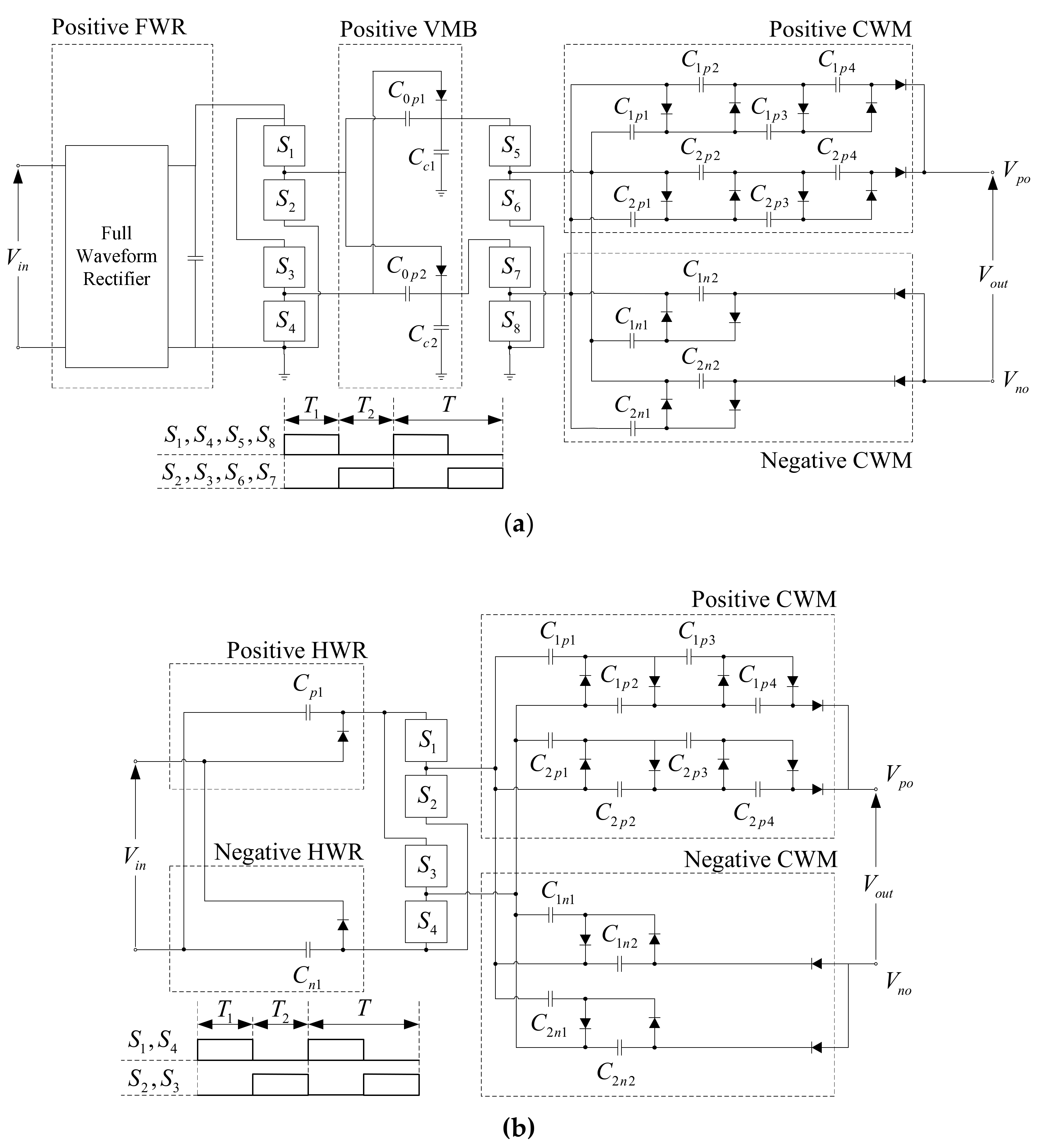
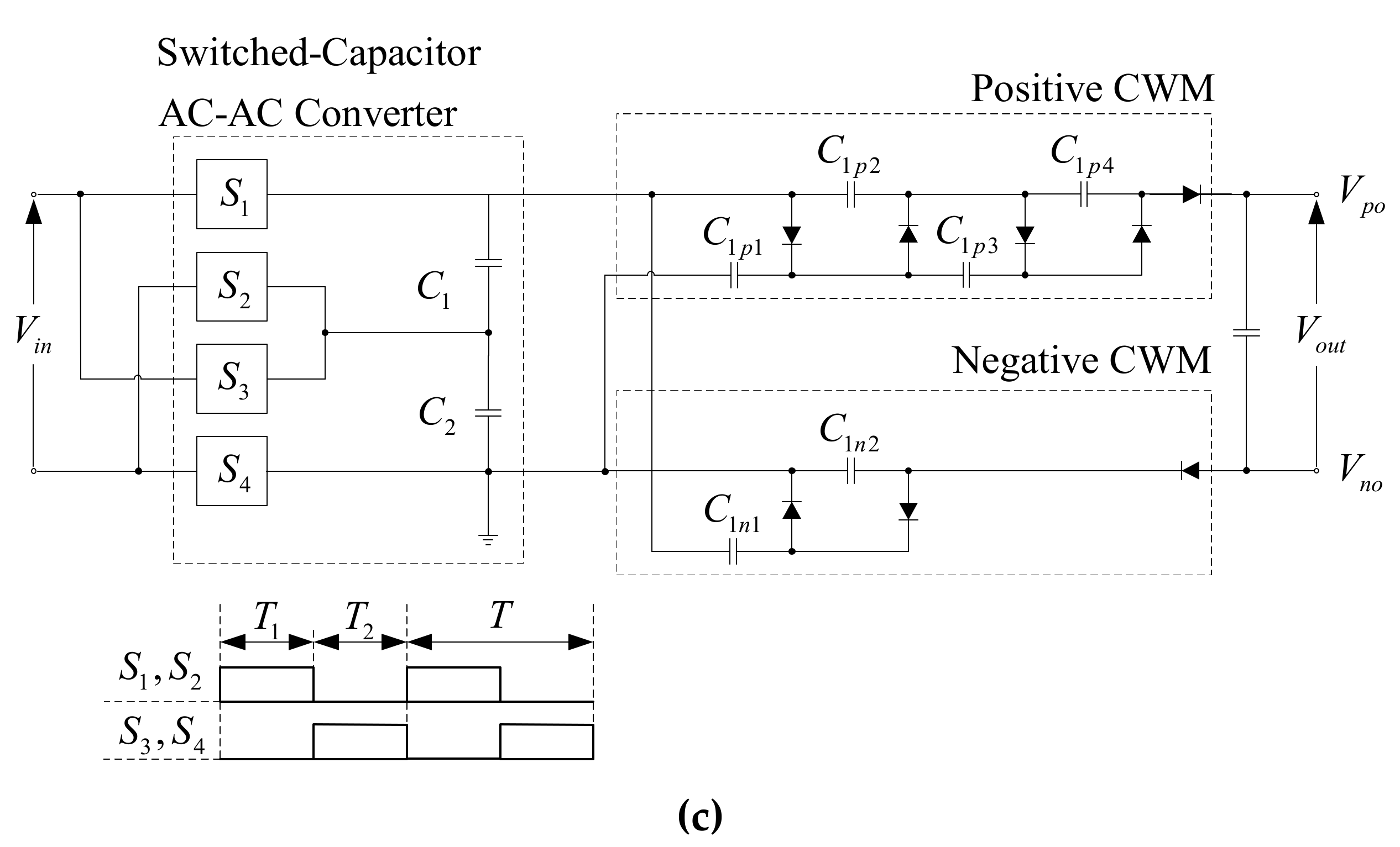
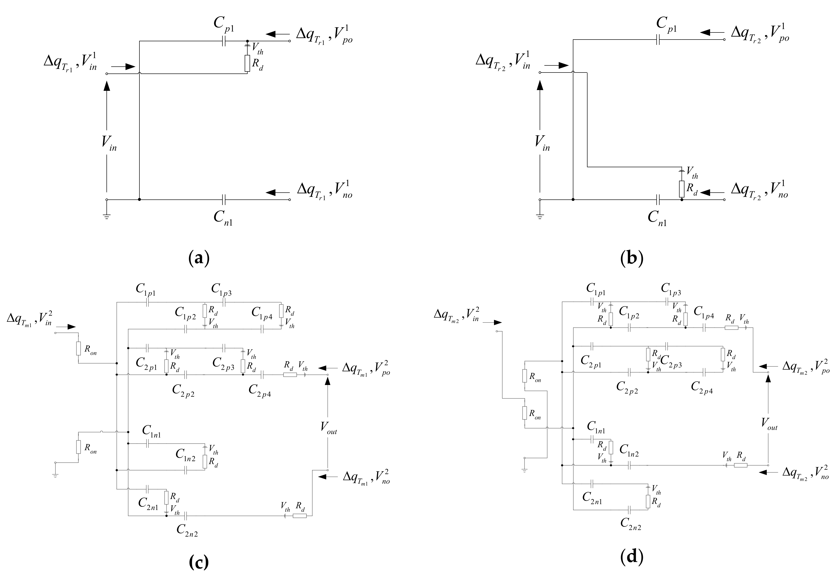
2. Proposed Modification

Figure 1 shows the topological diagrams of three modified HVMs in bipolar structure. Their sequential operations are digitally controlled by non-overlapping two-phase clock pulses, where T1 and T2 are the ‘on’ periods of the first and second clock signals, respectively, and T = T1 + T2 is the period of clock signals. The parameters Vin and Vout = VpoVno are the input peak value and the output peak value, respectively, Vpo is the positive output, and Vno is the negative output. In order to convert the 220 V and 50 Hz input into the DC output between 3.5 and 4.0 kV, the step-up gain of three proposed HVMs is set to 14. Each proposed HVM is designed to provide two amplification stages. The gains of the first and second amplification stages are equal to 2 and 7, respectively.
The circuit configuration of the first proposed HVM, referred to as HVM-A, is shown in Figure 1a. This modified scheme is based on the design technique suggested in [28]. The main parts are the positive full-wave rectifier (FWR), the positive voltage multiplier block (VMB), and the parallel-connected positive/negative CWMs. The positive VMB, positive CWM, and negative CWM have the gains of 2, 5, and 2, respectively. The DC input provided by the positive FWR is amplified by the positive VMB, and is then amplified again by the parallel-connected positive/negative CWMs. This means that the HVM-A provides two amplification stages. Figure 1b shows the circuit realization of the second proposed HVM, referred to as HVM-B, which is based on the design technique introduced in [10,12]. The main parts of the HVM-B are the positive/negative HWRs (or AC-DC rectifier) and the parallel-connected positive/negative CWMs. The gains of the AC-DC rectifier, positive CWM, and negative CWM are 2, 5, and 2, respectively. The DC input is provided and amplified by the AC-DC rectifier, and is then amplified again by the parallel-connected positive/negative CWMs. Similarly, the HVM-B exhibits two amplifications. The circuit configuration of the third proposed HVM, referred to as HVM-C, is depicted in Figure 1c. This configuration is based on the design technique proposed in [29]. The HVM-C consists of the switched-capacitor AC-AC converter and the positive/negative CWMs. The AC-AC converter, positive CWM, and negative CWM provide the gains of 2, 5, and 2, respectively. The AC input is amplified by the AC-AC converter, and is then amplified again and converted into the DC output by the positive/negative CWMs. Thus, the HVM-C also provides two amplifications.
Table 1 summarizes the outputs Vpo, Vno, and Vout of all proposed HVMs, where Vth denotes the forward threshold voltage of the diode. It is seen that the voltage outputs of the HVM-A and HVM-B are most affected by the diode switch non-idealities, whereas the voltage outputs of the HVM-C are less affected by the diode switch non-idealities. However, neglecting the small voltage Vth will cause the high DC output Vout of the three proposed HVMs to closely rise to 14Vin. Hence, the step-up gain of 14 can be achieved.

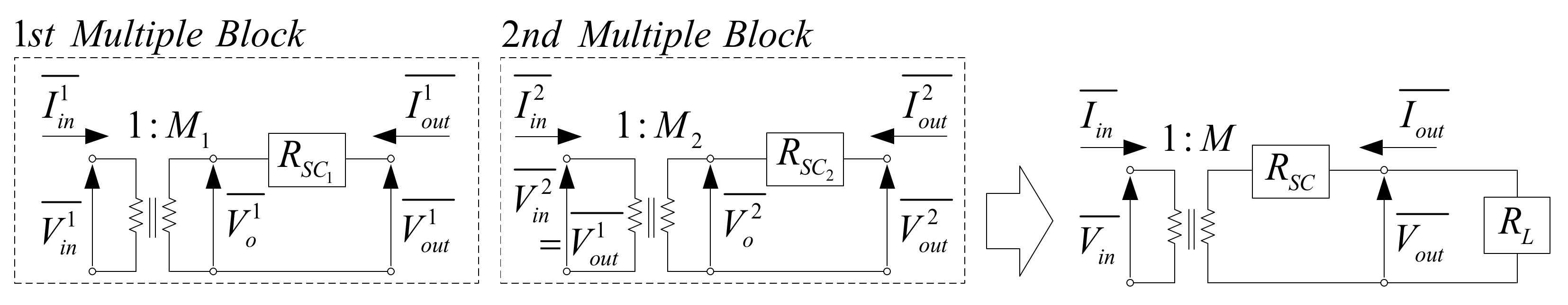
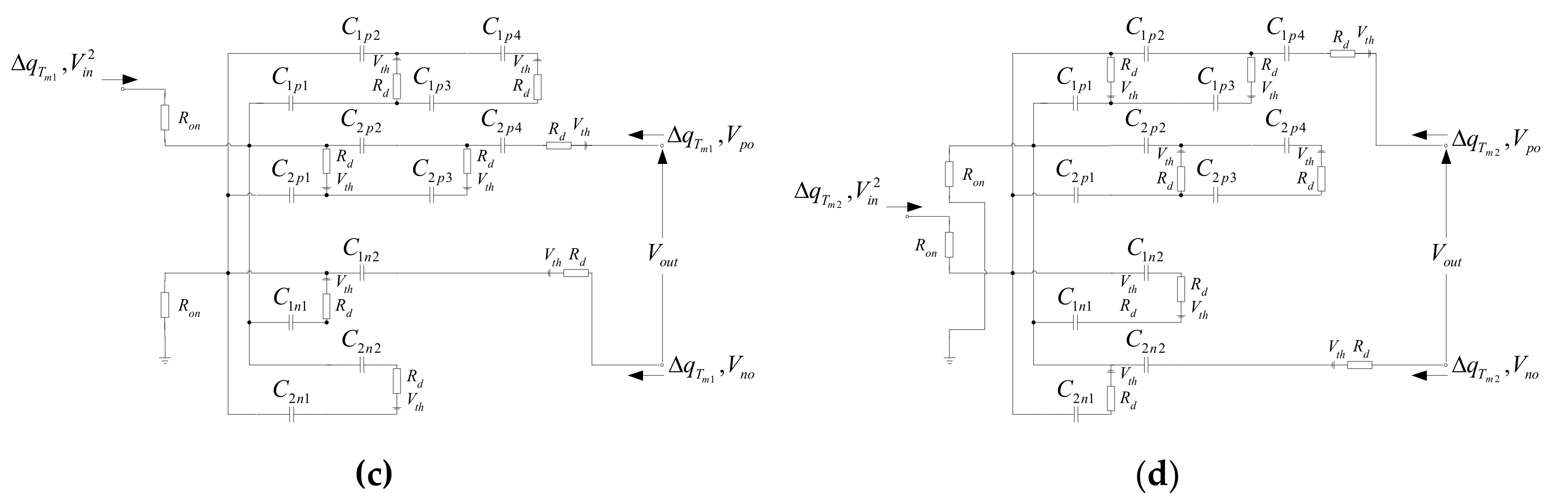
3. Theoretical Analysis

In order to provide ease of estimating and comparing the electrical characteristics of the proposed HVMs in practice, the simplified equivalent model, as shown in Figure 2, is theoretically derived. This equivalent model is a general equivalent circuit of capacitor-based converters [30,31]. It is composed of an ideal transformer with turn ratio (1: M), an internal resistance RSC, and an output load RL. To save space, only the analysis of the proposed HVM-A is described in detail under the following assumed conditions.
(1)
The dielectric loss is not considered.
(2)
The time constant of the proposed HVM-A is greater than the time period of clock pulses.
(3)
The input is a rectangular waveform.
The instantaneous equivalent circuits of HVM-A for State-Tri and State-Tmi (i = 1, 2) are shown in Figure 3a–d, respectively. The diode switch is represented as an ideal diode, an on-resistance (Rd), and a voltage source (Vth), while the transistor switch is modeled by the on-resistance (Ron). In steady state, the differential values of electric charges in C0pk (k = 1, 2), C1pq, C2pq (q = 1, 2, 3, 4), and C1nr, C2nr (r = 1, 2) can be written as
i = 1 2 Δ q T r i 0 p k = 0 ,   i = 1 2 Δ q T m i 1 p q = 0 ,   i = 1 2 Δ q T m i 2 p q = 0 ,   i = 1 2 Δ q T m i 1 n r = 0 , and i = 1 2 Δ q T m i 2 n r = 0 ,
where Δ q T r i 0 p k , Δ q T m i 1 p q , Δ q T m i 2 p q , Δ q T m i 1 n r , and Δ q T m i 2 n r denote the differential values of electric charges of the k-th, q-th, and r-th capacitors in State-Tri and State-Tmi, respectively, and the time interval of clock pulses satisfies the following conditions:
T r = i = 1 2 T r i , T m = i = 1 2 T m i   and   T r 1 = T r 2 = T r 2 , T m 1 = T m 2 = T m 2 .
The time interval Tr depends on the frequency of the AC input Vin, and the time interval Tm depends on the switching frequency for driving the transistor switch. Therefore, the relationship of differential values of electric charges in the input and output terminals ( Δ q T r 1 , V i n 1 , Δ q T r 2 , V i n 1 , Δ q T m 1 , V i n 2 , Δ q T m 2 , V i n 2 , Δ q T r 1 , V o , Δ q T r 2 , V o , Δ q T m 1 , V p o , Δ q T m 2 , V p o , Δ q T m 1 , V n o , and Δ q T m 2 , V n o ) for the symmetrical circuit structure in State-Tri and State-Tmi can be expressed as
State - T r 1     Δ q T r 1 , V i n 1 = Δ q T r 1 0 p 1 + Δ q T r 1 0 p 2   and   Δ q T r 1 , V o = Δ q T r 1 0 p 1
State - T r 2       Δ q T r 2 , V i n 1 = + Δ q T r 2 0 p 1 Δ q T r 2 0 p 2   and   Δ q T r 2 , V o = Δ q T r 2 0 p 2
State - T m 1       Δ q T m 1 , V i n 2 = Δ q T m 1 1 p 1 + Δ q T m 1 2 p 1 Δ q T m 1 2 p 2 Δ q T m 1 2 p 3 + Δ q T m 1 1 n 1 + Δ q T m 1 2 n 2 ,   Δ q T m 1 , V p o = Δ q T m 1 2 p 4   and   Δ q T m 1 , V n o = Δ q T m 1 2 n 2
State - T m 2       Δ q T m 2 , V i n 2 = Δ q T m 2 1 p 1 Δ q T m 2 1 p 2 Δ q T m 2 1 p 3 Δ q T m 2 2 p 1 + Δ q T m 2 1 n 2 + Δ q T m 2 2 n 1 ,   Δ q T m 2 , V p o = Δ q T m 2 1 p 4   and   Δ q T m 2 , V n o = Δ q T m 2 2 n 2 .
By using Kirchhoff’s current law, the input and output currents can respectively be written as
I i n ¯ = 1 T i = 1 2 Δ q T i , V i n = Δ q V i n T   and   I o u t ¯ = 1 T i = 1 2 Δ q T i , V o u t = Δ q V o u t T .
Substituting (3)–(6) into (7), the relation between the input current and the output current can be given by
I i n 1 ¯ = 2 I o u t 1 ¯ ,   I o u t 1 ¯ = I p o 1 ¯ = I n o 1 ¯   and   I i n 2 ¯ = 7 I o u t 2 ¯ ,   I o u t 2 ¯ = I p o 2 ¯ = I n o 2 ¯ .
From (8), the turn ratios M1 and M2 of Figure 2 are equal to 2 and 7, respectively. Thus, the consumed energy WT in one period of State-Tri and State-Tmi can be expressed as
W T r = W T r 1 + W T r 2 = 2 R d T r Δ q , V o u t 2 + 20 R o n T r Δ q , V o u t 2 ,   and        W T m = W T m 1 + W T m 2 = 16 R d T m Δ q , V o u t 2 + 164 R o n T m Δ q , V o u t 2 .
From (9), the consumed energy WT and the internal resistances RSC1 and RSC2 of the four-terminal equivalent model under the defined conditions can respectively be obtained as
W T = R S C Δ q V o u t 2 T
and      R S C 1 = 2 R d + 20 R o n   and   R S C 2 = 16 R d + 164 R o n .
From (11), the turn ratio (1: M) and internal resistance RSC can be calculated as
M = 14   and   R S C = 114 R d + 1144 R o n .
Therefore, the equivalent model of the proposed HVM-A can be expressed by the following matrix:
V i n ¯ I i n = 1 / 14 0 0 14 1 114 R d + 1144 R o n 0 1 V o u t ¯ I o u t .
From (13), the output voltage Vout, the output power Pout, and the power (or voltage) efficiency η for the proposed HVM-A of Figure 1a can be approximated to
V o u t = η × 14 × V i n ,   P o u t = ( V o u t ) 2 R L ,   and   η = R L R L + ( 114 R d + 1144 R o n ) .
From the above expressions, it should be noted that the outputs Vout and Pout as well as the power efficiency η are affected by the resistance values of Rd, Ron, and RL. The instantaneous equivalent circuits of the proposed HVM-B and HVM-C are depicted in Figure 4 and Figure 5, respectively. The theoretical analysis procedures for these two modified schemes follow the same analysis steps of the proposed HVM-A. The theoretical analysis results for comparing the internal resistance RSC of each modified scheme in the case of the step-up gain of 14 are summarized in Table 2.

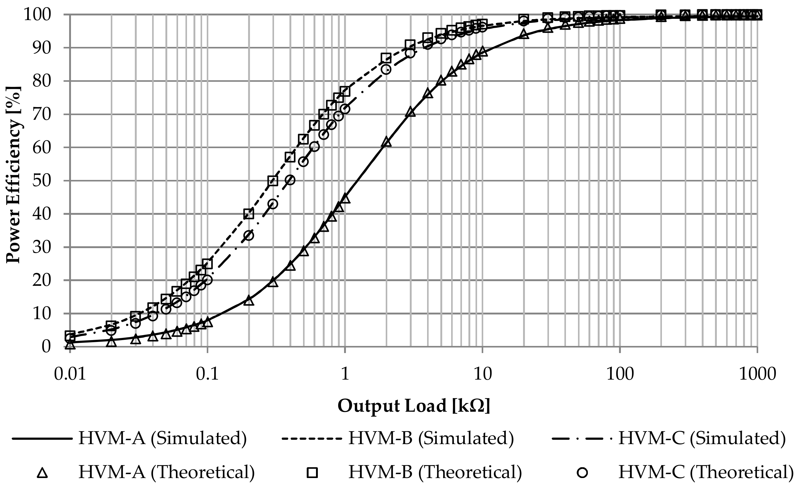
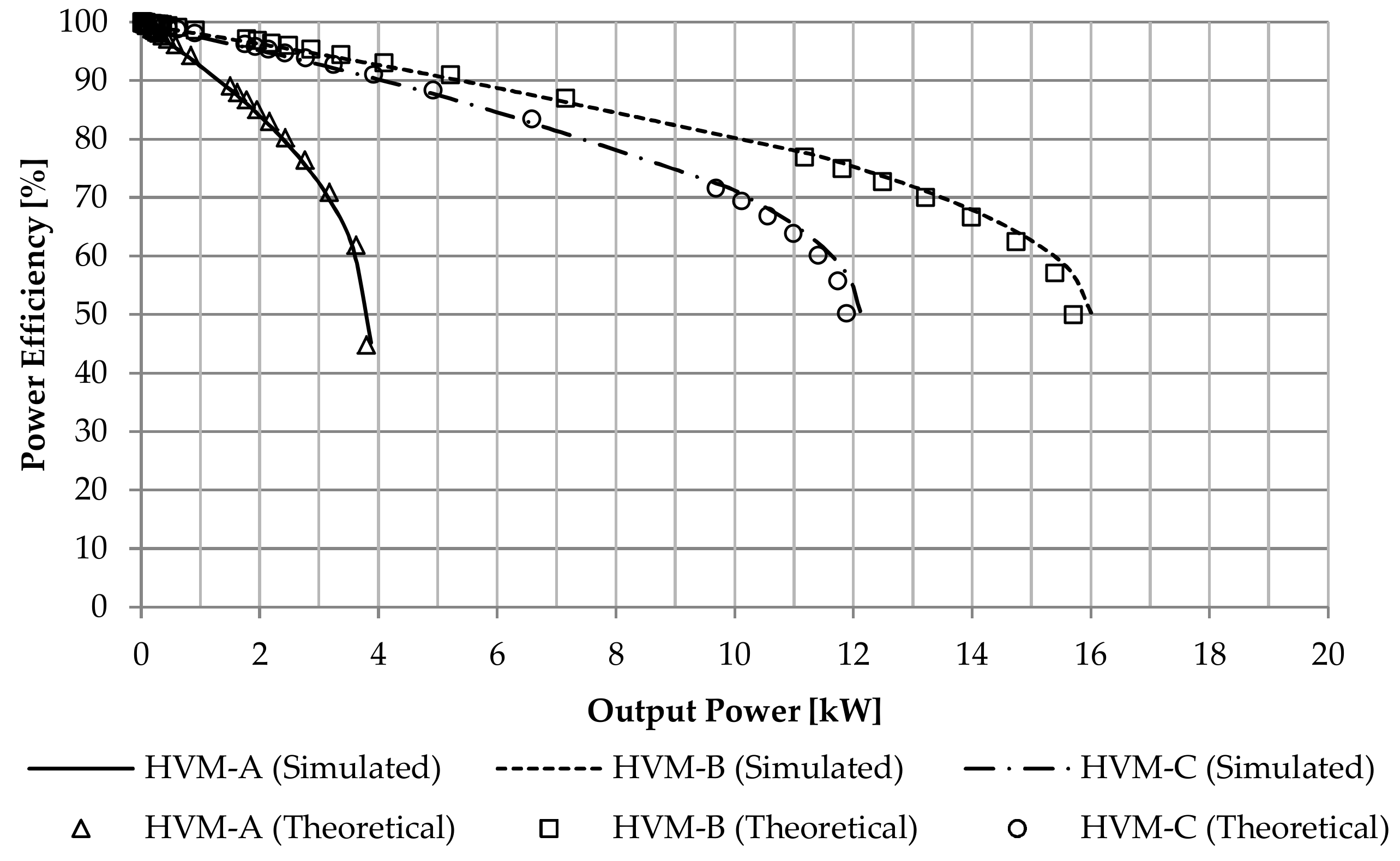
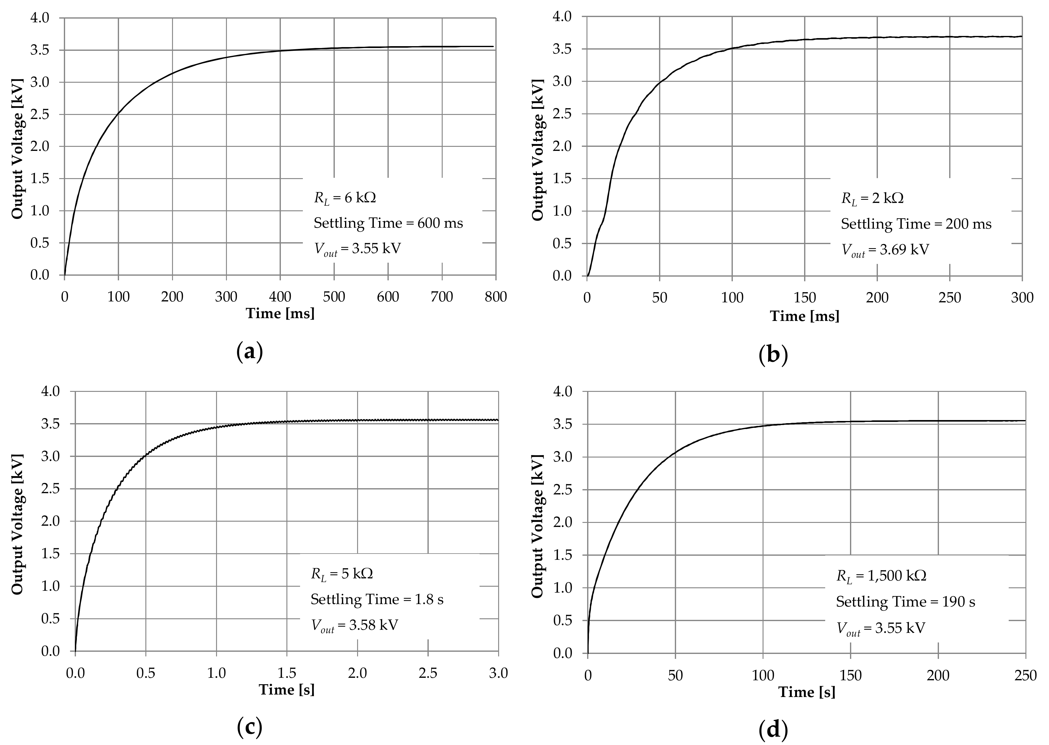
4. Simulation Results

To demonstrate the effectiveness of three proposed HVMs as well as the correctness of the given theoretical analysis, the modified schemes of Figure 1a–c were simulated with the SPICE program. In the simulations, the parameters were set to Vin = 220 V and 50 Hz, T1 = T2 = 100 µs, Ron = 1 Ω, and Cout = 100 µF. The results obtained from the simulations using SPICE and calculations using (14) are shown in Figure 6, Figure 7 and Figure 8.
Figure 6 illustrates the simulated and calculated values of the power efficiency of the HVM-A, HVM-B, and HVM-C when varying the value of the output load RL in the range of 0.01−1000 kΩ. In the case of setting RL = 5 kΩ, the simulated (calculated) values of the power efficiency of the proposed HVM-A, HVM-B, and HVM-C are approximately equal to 79.73% (80.19%), 93.85% (94.31%), and 92.16% (92.62%), respectively. In order to obtain the power efficiency greater than 80%, the values of RL for the HVM-A, HVM-B, and HVM-C should be greater than 6, 2, and 2 kΩ, respectively.
Figure 7 shows the variations of the output voltage with the output power, while Figure 8 shows the variations of the power efficiency with the output power. The HVM-A, HVM-B, and HVM-C provide the simulated (calculated) output power values of about 2.15 (2.17 kW), 7.08 (7.16 kW), and 6.52 kW (6.59 kW), respectively, when generating the output voltage of about 3.5 kV (or the power efficiency of about 80%). The average errors between the simulated values and the calculated values for the HVM-A, HVM-B, and HVM-C are approximated to 3.51%, 1.15%, and 1.98%, respectively. It is evident that the results from the simulations agree well with the results from the calculations from (14).
For comparison with the previous work, Figure 9a–c represents the simulated output voltages of the proposed HVM-A, HVM-B, and HVM-C, respectively, while Figure 9d represents the simulated output of the traditional CWM with seven stages [16]. In the performed simulations, the output load RL, shown in Figure 9, was selected to generate the target output voltage, such as 3.5 kV. From Figure 9a, the HVM-A can generate an output voltage of 3.55 kV within 600 ms when setting RL = 6 kΩ. The HVM-B can produce the output voltage of 3.69 kV within 200 ms in the case of RL = 2 kΩ, as shown in Figure 9b. From Figure 9c, the HVM-C can produce the output voltage of 3.58 kV within 1.8 s for setting RL = 5 kΩ. The traditional half-wave CWM [16] can generate an output voltage of 3.55 kV within 190 s for RL = 1500 kΩ, as illustrated in Figure 9d. It is obvious that the HVMs with different schemes can convert the 220 V and 50 Hz input into the DC output to have more than 3.5 kV within different settling time periods. This implies that the response speed values of the proposed HVMs and the traditional CWM [16] are different.

5. Discussion and Conclusions

To generate underwater shockwaves using electrical energy charge for non-thermal food processing, DC voltage in the range of 3.5–4.0 kV is required. The basic requirements for a good high-voltage multiplier (HVM) are high response speed, high voltage efficiency, and small number of components used. For utilizing the conventional Cockcroft–Walton-based HVMs with 100 V and 50 Hz or 100 V and 60 Hz proposed in [10,12,28,29] in the 220 V and 50 Hz power system, this paper presents a technique to modify their circuit realizations to be the new schemes that can apply the 220 V and 50 Hz input to produce the high DC output in the desired range.
Table 3 summarizes the realization methods of the three proposed HVMs (HVM-A, HVM-B, and HVM-C). The main sub-circuits for each modified scheme are given. Each modified scheme provides the step-up gain of 14. All proposed HVMs provide two cascaded stages to amplify the input signal, which are referred to as the first multiple block and second multiple block. The first amplification stage has a step-up gain of 2, while the second amplification stage has a step-up gain of 7. In order to enhance their response speed through bipolar structure realization [28,29], the output of the proposed HVMs can be provided by combining the outputs of the positive CWM and the negative CWM.
Table 4 shows the number of components used in the proposed HVMs and the traditional half-wave Cockcroft–Walton multiplier with seven stages [16], which include diodes, capacitors, and switches. It is seen that the proposed HVM-C uses the minimum number of devices in circuit implementation. On the other hand, the proposed HVM-A uses the maximum number of devices in circuit realization. By considering only the number of diodes used, it is found that the HVM-A and HVM-B consist of the highest number of diodes, whereas the HVM-C consists of the lowest number of diodes. The numbers of diodes shown in Table 4 support the comparison of the output voltages shown in Table 1. Moreover, the results from comparing the size, internal resistance, response speed, and power efficiency among the proposed HVMs and the traditional CWM [16] are summarized in Table 5. It is seen that not only the highest speed operations, but also the highest power (or voltage) efficiency can be provided in the proposed HVM-B. However, the HVM-A also provides a settling time of less than 1 s. From Table 5, among the three proposed HVMs, it is seen that the power efficiency is strongly dependent on the internal resistance RSC, which is in good agreement with the results shown in Table 2. By considering in terms of size of the circuit, the proposed HVM-C can be realized by using the smallest number of components. However, the settling time of the HVM-C is slower than that of HVM-A and HVM-B because the frequency of the input source is fixed at 50 Hz.
By converting the 220 V and 50 Hz input, all three proposed HVMs can produce the high DC output in the desired range of 3.5–4.0 kV. However, their electrical characteristics are different. This means that they can respond to the different requirements. The formulas given in this paper can be effectively used to estimate the circuit performances when designing the modified schemes because it appears from all figures that the simulation results are in good agreement with the theoretical values.
Lastly, to confirm the versatility of the proposed modification, the hardware implementation by using the modified high-voltage multiplier to generate underwater shockwaves for non-thermal food processing is the direction for future work.

Author Contributions

Conceptualization, K.E. and A.J. (Amphawan Julsereewong); methodology, A.J. (Anurak Jaiwanglok) and K.S.; writing—original draft preparation, A.J. (Anurak Jaiwanglok); writing—review and editing, K.E., K.S., and A.J. (Amphawan Julsereewong); project administration, A.J. (Amphawan Julsereewong). All authors have read and agreed to the published version of the manuscript.

Funding

This research received no external funding.

Conflicts of Interest

The authors declare no conflict of interest.

References

  1. Zhang, C.H.; Namihira, T.; Kiyan, T.; Nakashima, K.; Katsuki, S.; Akiyama, H.; Ito, H.; Imaizumi, Y. Investigation of Shockwave Produced by Large Volume Pulsed Discharge under Water. In Proceedings of the IEEE Pulsed Power Conference, Monterey, CA, USA, 13–15 June 2005; pp. 1377–1380. [Google Scholar]
  2. Yamashita, Y.; Oda, A.; Maehara, H.; Watanabe, T.; Motamedi, M.; Itoh, S. The numerical analysis of food processing using shock wave. Int. J. Multiphysics 2009, 3, 337–346. [Google Scholar] [CrossRef]
  3. Shimojima1, K.; Miyafuji, Y.; Naha1, K.; Higa, O.; Matsubara, R.; Higa, K.; Higa, Y.; Matsui, T.; Takemoto, A.; Tanaka, S.; et al. Development of the rice-powder manufacturing system using underwater shock wave. Int. J. Multiphysics 2012, 6, 355–363. [Google Scholar] [CrossRef]
  4. Shinzato, S.; Higa, Y.; Tamaki, T.; Iyama, H.; Itoh, S. Computational simulation of underwater shockwave propagation using smoothed particle hydrodynamics. Mater. Sci. Forum 2013, 767, 86–91. [Google Scholar] [CrossRef]
  5. Matsui, T.; Higa, K.; Matsubara, R.; Hanashiro, S.; Higa, O.; Itoh, S. Measurement of discharged energy and pressure of underwater shockwave changing materials of contact switch in high voltage power supply. Mater. Sci. Forum 2013, 767, 250–255. [Google Scholar] [CrossRef]
  6. Higa, O.; Matsubara, R.; Higa, K.; Miyafuji, Y.; Gushi, T.; Omine, Y.; Naha, K.; Shimojima, K.; Fukuoka, H.; Maehara, H.; et al. Mechanism of the shock wave generation and energy efficiency by underwater discharge. Int. J. Multiphysics 2012, 6, 89–97. [Google Scholar] [CrossRef]
  7. Higa, K.; Matsui, T.; Hanashiro, S.; Higa, O.; Itoh, S. Evaluation of the contact switch materials in high voltage power supply for generate of underwater shockwave by electrical discharge. Int. J. Multiphysics 2014, 8, 359–366. [Google Scholar] [CrossRef]
  8. Higa, O.; Yasuda, A.; Higa, Y.; Shimojima, K.; Hokamoto, K.; Itoh, S. Optical Examination of shockwave propagation induced by an underwater wire explosion. Int. J. Multiphysics 2016, 10, 343–354. [Google Scholar]
  9. Zhou, H.; Zhang, Y.; Han, R.; Jing, Y.; Wu, J.; Liu, Q.; Ding, W.; Qiu, A. Signal analysis and waveform reconstruction of shock waves generated by underwater electrical wire explosions with piezoelectric pressure probes. Sensors 2016, 16, 573. [Google Scholar] [CrossRef] [Green Version]
  10. Eguchi, K.; Jaiwanglok, A.; Julsereewong, A.; Asadi, F.; Abe, H.; Oota, I. Design of a non-thermal food processing system utilizing wire discharge of dual electrodes in underwater. IJICIC 2018, 14, 847–860. [Google Scholar]
  11. Abe, H.; Do, W.; Eguchi, K. An Efficient Non-Thermal Food Processing System by Underwater Shockwaves Using Two Pairs of Restoration Electrodes. In Proceedings of the 5th International Conference on Engineering, Applied Sciences and Technology, Luang Prabang, LAOS, 2–5 July 2019; pp. 1–4. [Google Scholar]
  12. Abe, K.; Ogata, R.; Eguchi, K.; Smerpitak, K.; Pongswatd, S. Study on non-thermal food processing utilizing an underwater shockwave. Indian J. Sci.Technol. 2017, 10, 1–5. [Google Scholar] [CrossRef]
  13. Kuraya, E.; Nakada, S.; Touyama, A.; Itoh, S. Improving the antioxidant functionality of Citrus junos Tanaka (yuzu) fruit juice by underwater shockwave pretreatment. Food Chem. 2017, 216, 123–129. [Google Scholar] [CrossRef] [PubMed]
  14. Eguchi, K.; Terada, S.; Oota, I. Design of a digitally controlled inductor-less voltage multiplier for non-thermal food processing. IJIEE 2014, 4, 438–445. [Google Scholar]
  15. Lamantia, A.; Maranesi, P.; Radrizzani, L. The Dynamic of the Cockcroft-Walton Voltage Multiplier. In Proceedings of the 21st Annual IEEE Conference on Power Electronics Specialists, San Antonio, TX, USA, 11–14 June 1990; pp. 485–490. [Google Scholar]
  16. Lamantia, A.; Maranesi, P.G.; Radrizzani, L. Small-signal model of the Cockcroft–Walton voltage multiplier. IEEE Trans. Power Electron 1994, 9, 18–25. [Google Scholar] [CrossRef]
  17. Kobougias, I.C.; Tatakis, E.C. Optimal design of a half-wave Cockcroft–Walton voltage multiplier with minimum total capacitance. IEEE Trans. Power Electron 2010, 25, 2460–2468. [Google Scholar] [CrossRef]
  18. Katzir, L.; Shmilovitz, D. Effect of the capacitance distribution on the output impedance of the half-wave Cockcroft-Walton voltage multiplier. In Proceedings of the 2016 IEEE Applied Power Electronics Conference and Exposition, Long Beach, CA, USA, 20–24 March 2016; pp. 3655–3658. [Google Scholar]
  19. Tanzawa, T. Innovation of switched-capacitor voltage multiplier: Part 1: A brief history. IEEE Solid-State Circuits Mag. 2016, 8, 51–59. [Google Scholar] [CrossRef]
  20. Park, S.; Yang, J.; Rivas-Davila, J. A hybrid Cockcroft-Walton/Dickson multiplier for high voltage generation. IEEE Trans. Power Electron 2020, 35, 2714–2723. [Google Scholar] [CrossRef]
  21. Abe, K.; Sasaki, H.; Oota, I.; Eguchi, K. Improvement of an output voltage efficiency of a high voltage generator for non-thermal food processing systems. ICIC Express Lett. 2015, 9, 3087–3092. [Google Scholar]
  22. Young, C.M.; Chen, M.H.; Chang, T.A.; Ko, C.C.; Jen, K.K. Cascade Cockcroft–Walton voltage multiplier applied to transformerless high step- up DC–DC converter. IEEE Trans. Ind. Electron. 2013, 60, 523–537. [Google Scholar] [CrossRef]
  23. Razzak, M.A.; Chakraborty, S.; Tasneem, Z. Design of a multistage 0.1/12 kV DC-DC matrix converter using Cockcroft-Walton voltage multiplier topology. Proceeding of the 2015 IEEE International WIE Conference on Electrical and Computing Engineering, Dhaka, Bangladesh, 19–20 December 2015; pp. 309–312. [Google Scholar]
  24. Iqbal, S.; Besar, R. A bipolar Cockcroft-Walton voltage multipliers for gas lasers. Am. J. Appl. Sci. 2007, 4, 793–799. [Google Scholar] [CrossRef] [Green Version]
  25. Iqbal, S. A hybrid symmetrical voltage multiplier. IEEE Trans. Power Electr. 2014, 29, 6–12. [Google Scholar] [CrossRef]
  26. Eguchi, K.; Pongswatd, S.; Terada, S.; Oota, I. Parallel-connected high voltage multiplier with symmetrical structure. Appl. Mech. Mater. 2014, 619, 173–177. [Google Scholar] [CrossRef]
  27. Eguchi, K.; Abe, K.; Terada, S.; Oota, I. A parallel-connected high voltage multiplier for non-thermal food processing. In Proceedings of the 7th International Conference on Electrical, Electronics and Civil Engineering, Pattaya, Thailand, 17–18 June 2015; pp. 14–18. [Google Scholar]
  28. Eguchi, K.; Abe, K.; Fujisawa, H.; Oota, I. Design of a High Voltage Multiplier with Series-Connected Bipolar Topology. In Proceedings of the Third International Conference on Advances in Applied Science and Environmental Technology, Bangkok, Thailand, 28–29 December 2015; pp. 113–117. [Google Scholar]
  29. Eguchi, K.; Wongjan, A.; Julsereewong, A.; Do, W.; Oota, I. Design of a high-voltage multiplier combined with Cockcroft-Walton voltage multipliers and switched-capacitor AC-AC converters. IJICIC 2017, 13, 1007–1019. [Google Scholar]
  30. Tsubomi, K.; Terada, S.; Eguchi, K.; Oota, I. Improvement and analysis of equivalent circuit for switching converter by considering power loss. Trans. IEICE C 2014, 97, 365–375. [Google Scholar]
  31. Eguchi, K.; Junsing, T.; Julsereewong, A.; Do, W.; Oota, I. Design of a nesting-type switched-capacitor AC/DC converter using voltage equalizers. IJICIC 2017, 13, 1369–1384. [Google Scholar]
Figure 1. Modified schemes of three proposed high-voltage multipliers (HVMs): (a) HVM-A; (b) HVM-B; (c) HVM-C.
Sustainability 12 06330 g001aSustainability 12 06330 g001b
Figure 2. Simplified equivalent model of the proposed HVMs.
Sustainability 12 06330 g002
Figure 3. Instantaneous equivalent circuits of HVM-A: (a) State-Tr1; (b) State-Tr2; (c) State-Tm1; (d) State-Tm2.
Sustainability 12 06330 g003aSustainability 12 06330 g003b
Figure 4. Instantaneous equivalent circuits of HVM-B: (a) State-Tr1; (b) State-Tr2; (c) State-Tm1; (d) State-Tm2.
Sustainability 12 06330 g004
Figure 5. Instantaneous equivalent circuits of HVM-C: (a) State-Tr1; (b) State-Tr2; (c) State-Tm1; (d) State-Tm2.
Sustainability 12 06330 g005
Figure 6. Simulated and calculated values of the power efficiency by varying the output load value.
Sustainability 12 06330 g006
Figure 7. Variations of the output voltage with the output power.
Sustainability 12 06330 g007
Figure 8. Variations of the power efficiency with the output power.
Sustainability 12 06330 g008
Figure 9. Simulated output voltages: (a) HVM-A; (b) HVM-B; (c) HVM-C; (d) Cockcroft–Walton multiplier (CWM) [16].
Sustainability 12 06330 g009
Table 1. Comparison of the positive output, negative output, and output voltage.
Modified SchemeVpoVnoVout
HVM-AVpo = 10Vin − 11VthVno = 4Vin − 4VthVout = 14Vin − 15Vth
HVM-BVpo = 10Vin − 11VthVno = 4Vin − 4VthVout = 14Vin − 15Vth
HVM-CVpo = 10Vin − 6VthVno = 4Vin − 3VthVout = 14Vin − 9Vth
Table 2. Comparison of internal resistance Rsc of the proposed HVMs for step-up gain of 14.
Modified SchemeStep-Up GainRSC
HVM-A14114Rd + 1144Ron
HVM-B14114Rd + 132Ron
HVM-C148Rd + 392Ron
Table 3. Summary of main parts used in the proposed HVMs.
Modified Scheme1st Multiple Block2nd Multiple Block
HVM-APositive FWRParallel-Connected Positive CWM
Positive VMBParallel-Connected Negative CWM
HVM-BPositive/Negative HWRsParallel-Connected Positive CWM
(AC-DC Rectifier)Parallel-Connected Negative CWM
HVM-CPositive/Negative VMBsPositive CWM
(SC AC-AC Converter)Negative CWM
Table 4. Comparison of the numbers of components used in the proposed HVMs.
Modified SchemeDiodeCapacitorSwitchTotal
HVM-A1816842
HVM-B1814436
HVM-C88420
Traditional CWM [16]1414-28
Table 5. Summary of comparison results.
Modified SchemeSizeInternal ResistanceResponse SpeedEfficiency
HVM-A4423
HVM-B3211
HVM-C1332
Traditional CWM [16]2144
1: Best–4: Worst.

