Article

Dual-Frequency Programmed Harmonics Modulation-based Simultaneous Wireless Information and Power Transfer System via a Common Resonance Link

1
School of Electrical and Information Engineering, Zhengzhou University of Light Industry, Zhengzhou 450002, China
2
Faculty of Electrical Engineering and Computer Science, VŠB-Technical University of Ostrava, Poruba-Ostrava 70032, Czech Republic
*
Authors to whom correspondence should be addressed.
Sustainability 2020, 12(10), 4189; https://doi.org/10.3390/su12104189
Submission received: 8 March 2020 / Revised: 9 May 2020 / Accepted: 11 May 2020 / Published: 20 May 2020

Abstract

:
Most simultaneous wireless information and power transmission (SWIPT) systems currently operate at a single frequency, where the power and information transmission affect the resonance state of each other. This paper proposes a structure using dual-frequency programmed harmonics modulation (DFPHM). The primary-side inverter outputs a dual-frequency (DF) wave containing the power transmission and information transmission frequencies, while the DF wave is coupled to the secondary side through a common inductive link. After the power and information are transmitted to the secondary side, they are demodulated in different branches. Wave trappers are designed on each branch to reduce the interference of information transmission on power transmission. There is no tight coupling transformer in the system to inject information, so the system order is not high. Experiments verified that the proposed structure based on DFPHM is effective.

1. Introduction

In recent years, simultaneous wireless information and power transmission (SWIPT) systems have become an emerging research area [1,2]. SWIPT technology has been applied in domains such as transportation [3], medical equipment [4,5], particular environments [6,7,8], and so on. For example, Vehicle-to-Grid (V2G) is a typical SWIPT application; it provides many services such as reactive power compensation, voltage regulation, harmonic filtering, and primary frequency control [9]. The SWIPT system exchanges information such as the primary and secondary voltage, power, and temperature while transmitting power [10]. It also feedbacks the battery state of wireless charging systems through the reverse transmission of information [11]. Therefore, the system requires the simultaneous wireless transmission of power and information between wireless charging electric vehicles and the power grid.
There are two main ways to transmit wireless power and information simultaneously [12,13,14]. The first is that information and power are on different physical channels [12]. They go through different transmission coils, that is, information and power are separated from the physical channel to achieve wireless transmission. The second is that information and power are in the same physical channel [13,14], and only one set of inductive coupling coils is used to synchronize the transmission of information and power through a modulation strategy.
The first method requires a communication coil and corresponding modulation and demodulation circuits on the primary and secondary sides, which increases the number of system components. Also, there is interference between the power channel and the information channel, which increases the bit error rate [15]. Finally, energy transmission is interrupted during information modulation, which affects the stability of electrical energy transmission.
The second method combines the signal with the power transmission. The SWIPT system transmitting multiple frequencies simultaneously has advantages in terms of standard compatibility, cost, and volume. On one hand, there are multiple charging standards in the field of wireless charging, and the transmission frequency prescribed by each is not uniform. In the Qi standard, two transmission frequencies are specified: one for transmitting power and the other for information. Therefore, if multi-frequency SWIPT technology can be compatible with the transmission frequency requirements of different standards, it will definitely bring great convenience to consumers. On the other hand, a multi-frequency SWIPT system does not require additional information channels, thereby simplifying the system structure and helping to reduce the size and cost of the system. Therefore, multifrequency SWIPT is a technology with great potential.
At present, SWIPT systems with shared coupling channels mostly use tightly coupled transformers to inject information into the power transmission channel. When information is transmitted bidirectionally, up to four transformers are used for information injection and demodulation [16], which will undoubtedly raise the order of the system, make the coupling process complicated, and increase the system volume. Dual-frequency programmed harmonics modulation (DFPHM) is a good way to solve this problem [17,18,19], and has been applied in the field of wireless power transfer (WPT). In the approach proposed in this paper, there is only one inverter on the primary side, which outputs a PWM voltage wave with two frequencies at the same time, and simultaneously transmits two frequencies to the secondary via a common inductive link. The two frequency waves are then demodulated in the power and information channels of the secondary side, and the number of coupling loops is greatly reduced.
However, when DFPHM is used in a SWIPT system, it still faces some challenges. In SWIPT systems, the fundamental is usually used to transmit power, and the higher harmonics are used to transmit information. If a harmonic frequency is close to the fundamental, e.g., the 3rd or 5th harmonic [17,18], it will have an adverse effect on power transmission and reduce the information transmission rate. DFPHM removes the tight coupling transformer of the information transmitter, but the tight coupling receiver still makes the system structure complicated [19]. This paper proposes a SWIPT structure without a tight coupling receiver by using DFPHM. In this structure, there is only one inverter on the primary side; the two frequencies of power and information transmission are simultaneously transmitted to the secondary side via a common inductive link. The frequencies are decoupled in their respective transmission channels by wave trappers. The wave trapper is equivalent to an open circuit at resonance, so it can be ignored when analyzing the corresponding channel, and the order of the entire system is not very high.
The paper is organized as follows. Section 2 provides an overview of the system and describes the principle of dual-frequency programmed harmonic modulation. Section 3 analyzes the wave trapper. In Section 4, the power transmission and information demodulation are verified by experiments. Section 5 presents the conclusion.

2. System Structure and Principle

2.1. System Structure

The circuit diagram of the proposed SWIPT system is shown in Figure 1. The light purple block represents the transmitting side, and the light blue block indicates the receiving side. The inverter generates waveforms of frequencies ω a and ω b . On the primary side, the L p acts as an inductor to form two frequency paths with C p a and C p b , respectively. On the secondary side, L s , C s a and C s b form two paths receiving power and information, respectively. In each branch, there is a wave trapper (noted as WT 1 , WT 2 , WT 3 and WT 4 in Figure 1) composed of a parallel resonant tank to block undesired frequencies. R A and R B represent the load of power and information branch, respectively.
The wave trapper has a blocking effect on the target frequency, while the nontarget frequency can still pass [16]. The influence of the wave trapper needs to be considered when determining the values of the four compensation capacitors C p a , C p b , C s a and C s b in the four frequency channels, so that resonance occurs when the target frequency flows through the paths. Table 1 shows the resonance frequencies of the corresponding branches and the cut-off frequencies of the wave trappers.
In the proposed SWIPT structure, the different frequency waves flow through different channels. As shown in Figure 2, the red path resonates at frequency ω a , where the wave trapper cuts off frequency ω b . Meanwhile, the blue path resonates at frequency ω b , where the wave trapper cuts off frequency ω a . Therefore, the power with frequency ω a flows in the red channel, and the signals with frequency ω b flow through the blue channel.

2.2. System Operation Principle

There is only one inverter on the primary side, which outputs a dual-frequency wave, i.e., one for transmitting power, and one for transmitting information, so the entire system works in a joint operating mode of two frequencies

2.2.1. DFPHM Switching Angles

Figure 3 shows the structure diagram of the dual-frequency (DF) inverter. Using a FPGA controller, the dual-frequency switching signals are modulated onto the active bridge; then, the DF-inverter outputs a dual frequency wave which can be regarded as the superposition of two frequency waves. In the inverter, the actions of MOSFETs S1 and S4 (marked in red), and MOSFETs S2 and S3 (marked in blue) are synchronized.
The Fourier expansion of the quarter symmetric unipolar waveform is
ν ( ω t ) = n = 1 , 3 , 5 4 V d c n π [ c o s ( n θ 1 ) c o s ( n θ 2 ) + c o s ( n θ 3 ) + c o s ( n θ m ) ] s i n ( n ω t )
According to the principle of Fourier series, a periodic square wave signal can be formed by superimposing a series of sine waves at the integer multiple of the frequency. By controlling the coefficients of s i n ( n ω t ) in (1), the different frequency sine wave components of the Fourier series are controlled. The coefficients of Fourier expansion of DFPWM can be expressed as
{ 4 V d c π ( 1 2 c o s θ 1 + 2 c o s θ 2 + 2 c o s θ m ) = V L F 4 V d c 3 π ( 1 2 c o s 3 θ 1 + 2 c o s 3 θ 2 + 2 c o s 3 θ m ) = 0 4 V d c ( 2 k 1 ) π [ 1 2 c o s ( 2 k 1 ) θ 1 + 2 c o s ( 2 k 1 ) θ 2 + 2 c o s ( 2 k 1 ) θ m ] = V H F 4 V d c n π ( 1 2 c o s n θ 1 + 2 c o s n θ 2 + 2 c o s n θ m ) = 0
where θ represents the turn-on and turn-off moment, m represents the number of switching angles, and V L F and V H F are the amplitude voltage of the waveforms at low and high frequencies, respectively, as shown in Figure 3. The 2 k 1 term represents the general term of the amplitude with an arbitrary order of harmonics. The solution of Equation (2) can be found using the evolution algorithm [20].
The solution θ m of formula (2) is the sequence of switching angles in a quarter cycle, as shown in Figure 4 in the yellow marked area. The sequence of switching angles for the rest of the cycle can be obtained according to symmetry. Then, the inverter generates a set of dual-frequency waves when working with this set of switching angles.

2.2.2. Dual-Mode Operation

In this study, dual-mode refers to a 5 kHz and 185 kHz joint operation mode. Power is continuously transmitted at a frequency of 5 kHz. Information is transmitted in OOK or 2ASK mode [21,22]. As shown in Figure 5, the system operates alternately in two sets of modes. The pink area indicates that the system outputs dual frequency signals in DFPHM mode with digital 1. When transmitting digital 1, a frequency of 185 kHz is superimposed on a frequency of 5 kHz. The blue area indicates that the system is operating in single frequency mode with digital 0. When transmitting digital 0, the inverter only outputs the frequency of 5 kHz.
In the joint operation mode, the two frequencies of power and information are demodulated in their respective transmission channels. When transmitting signals 1 and 0, the transmission of the 5 kHz power wave is not affected, so power transmission is not influenced by information transmission in this joint operation mode.
On the secondary side, receiving the binary data signal requires a data demodulation module. In Figure 1, the data demodulation module is represented by R B . The circuit of the data demodulation module is shown in Figure 6. The voltage of R B in Figure 1 is the input voltage of the demodulation module V R B . The light green area in Figure 6 represents the band-pass filter. The pass frequency of the band-pass filter is around 185 kHz, which eliminates power harmonics at 5 kHz, as well as undesired higher harmonics. The voltage waveform output by the band-pass filter is the input voltage of the envelope detector, which is marked in the red block. To get a smoother waveform, the envelope passes through a low-pass filter. The low-pass filter is marked with light blue in the figure. The voltage amplitude at this time is very low, so an amplifier, marked with orange in the figure, is needed to make the comparator more effective. Finally, the waveform output by the amplifier becomes a binary square wave signal under the action of the comparator.

3. System Parameter Design

In the circuit shown in Figure 1, the bridge inverter controlled by DFPWM outputs dual frequency signals. Therefore, two AC voltage sources connected in series represent the DF-inverter in Figure 1, which results in an equivalent circuit to that shown in Figure 7. The four wave trappers are noted as WT 1 , WT 2 , WT 3 and WT 4 .

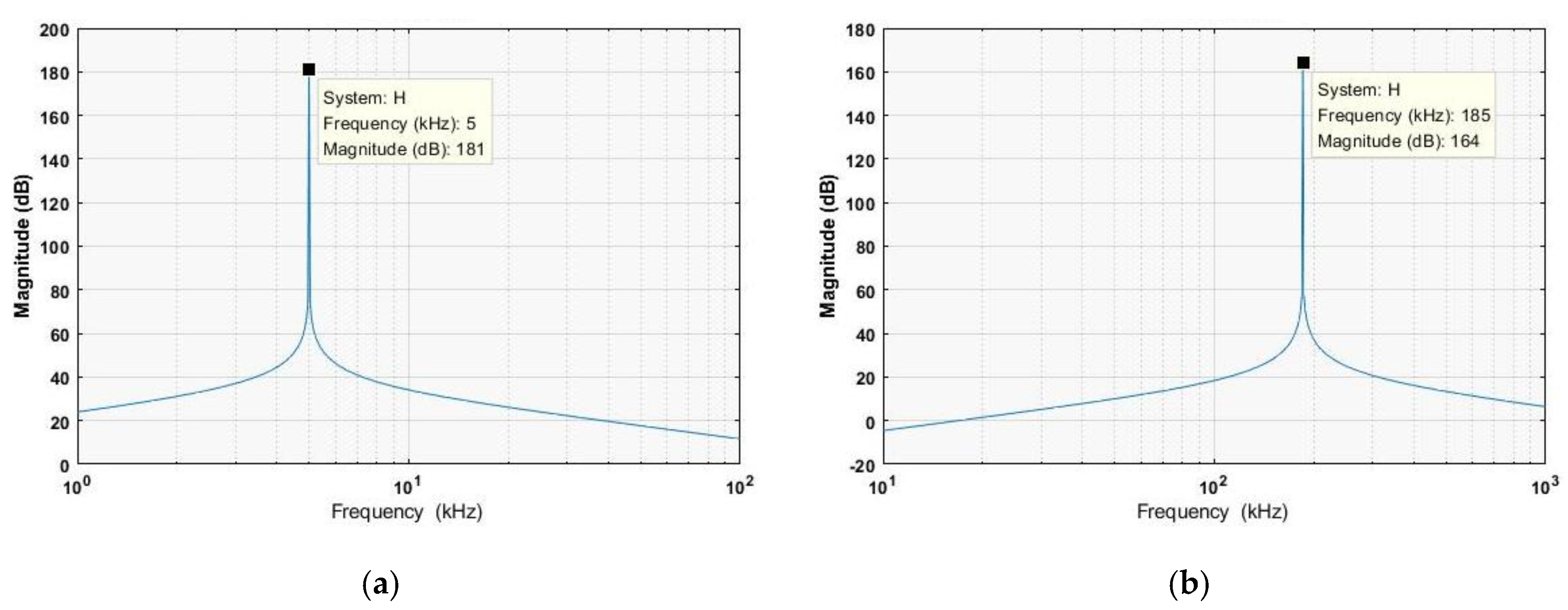
3.1. Wave Trappers Design

In Figure 7, the AC sources in series produce a composite wave of two frequencies, ω a and ω b , where ω a is used for power transmission and ω b for information transmission.
ω a < ω b
According to the relationship between the wave trapper and the cut-off frequency in Table 1, the following equations hold
{ L k s a C k s a = 1 ω b 2 L k p a C k p a = 1 ω b 2 L k s b C k s b = 1 ω a 2 L k p b C k p b = 1 ω a 2
According to the constraints of formula (4), considering the relationship between the branch resonance frequency and the wave trapper in Table 1, parameters WT 1 and WT 2 on the primary side can be obtained as
L k p a = 1 ω a 2 L p C p a ω a 2 C p a ( 1 ω a 2 ω b 2 )
C k p a = ω a 2 C p a ( 1 ω a 2 L p C p a ) × ( ω b 2 ω a 2 )
L k p b = 1 ω b 2 L p C p b ω b 2 C p b ( 1 ω b 2 ω a 2 )
C k p b = ω b 2 C p b ( 1 ω b 2 L p C p b ) × ( ω a 2 ω b 2 )
Similarly, parameters of WT 3 and WT 4 on the secondary side can be obtained as
L k s a = 1 ω a 2 L s C s a ω a 2 C s a ( 1 ω a 2 ω b 2 )
C k s a = ω a 2 C s b ( 1 ω a 2 L s C s a ) × ( ω b 2 ω a 2 )  
L k s b = 1 ω b 2 L s C s b ω b 2 C s b ( 1 ω b 2 ω a 2 )
C k s b = ω b 2 C s b ( 1 ω b 2 L s C s b ) × ( ω a 2 ω b 2 )
The above formulas (5)–(12) are the parameters of the wave trappers; they must be positive. Combined with the constraint of formula (3), the value range of the compensation capacitors are obtained:
{ C p a < 1 ω a 2 L p C p b > 1 ω b 2 L p C s a < 1 ω a 2 L s C s b > 1 ω b 2 L s
According to the above relationships, when the L p , L s , ω a , and ω b are determined, the compensation capacitors of each branch can be obtained by (13). Subsequently, the parameters of the wave trappers on each branch are determined by (4)–(12).

3.2. Analysis of Impedance

The equivalent AC power generates the two different frequencies waves of ω a and ω b . In order to verify the function of the wave trappers, the impedance of each branch is deduced as follows.
On the primary side, the impedance of the low-frequency branch working in ω a is
Z p a ( ω ) = 1 j ω C p a + Z k p a
The impedance in the branch working in ω b is
Z p b ( ω ) = 1 j ω C p b + Z k p b
The impedance of WT 1 is Z k p a . The impedance of WT 2 is Z k p b . According to (14) and (15), at the different working frequencies, the Z k p a and Z k p b have different values:
Z k p a ( ω ) = 1 1 j ω L k p a + j ω C k p a
Z k p b ( ω ) = 1 1 j ω L k p b + j ω C k p b
On the secondary side, the impedances of the two branches are
Z s a ( ω ) = 1 j ω C s a + Z k s a
Z s b ( ω ) = 1 j ω C s b + Z k s b
where Z k s a and Z k s b are the impedances of WT 3 and WT 4 .
Z k s a ( ω ) = 1 1 j ω L k s a + j ω C k s a
Z k s b ( ω ) = 1 1 j ω L k s b + j ω C k s b
In the Bode diagram of impedance at different frequencies, shown in Figure 8, the impedances corresponding to each wave trapper reach their peak values at the cut-off frequency. Consequently, the wave trappers reduce the undesired harmonics on each branch while blocking the mutual interference between the two channels.

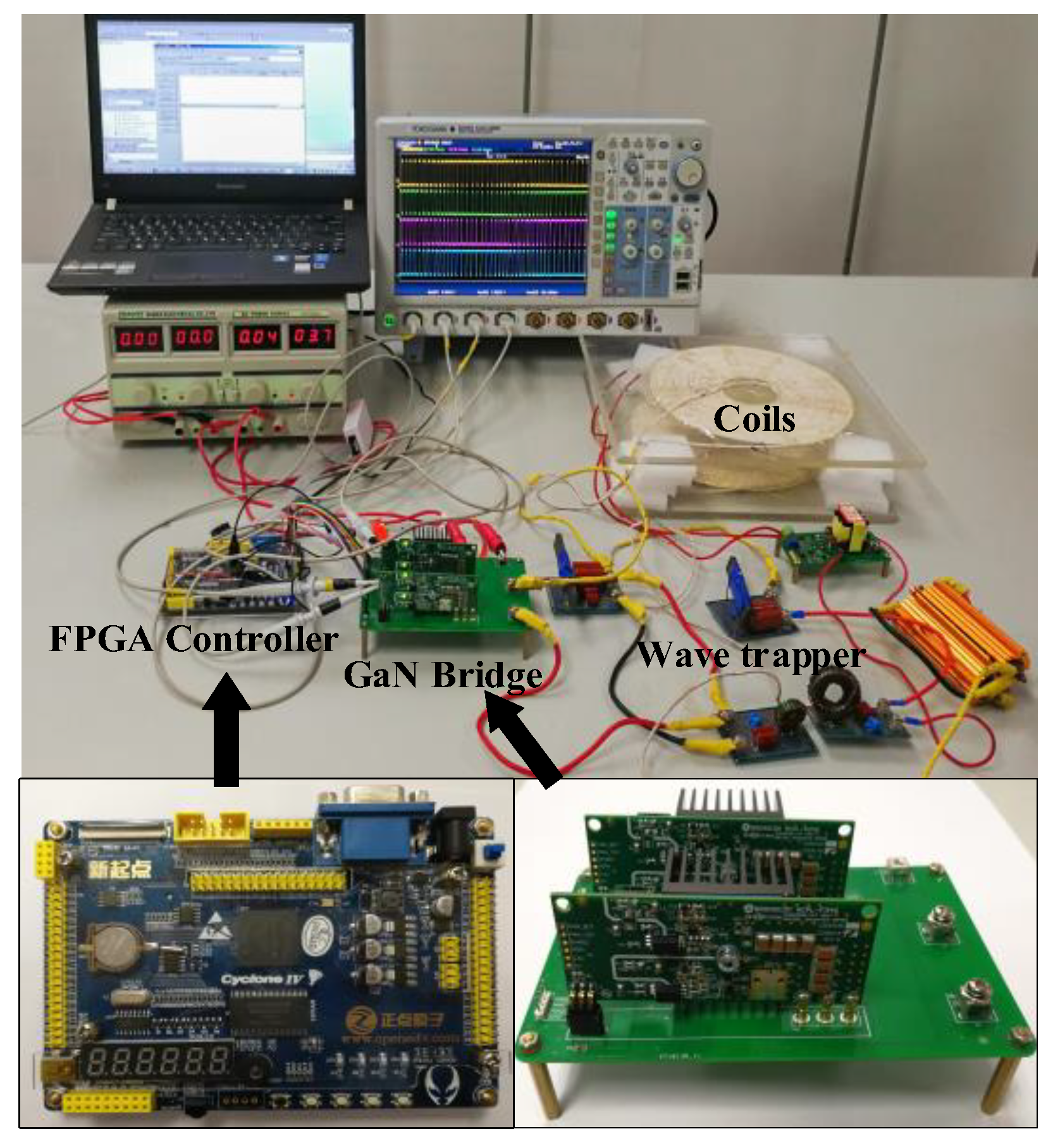
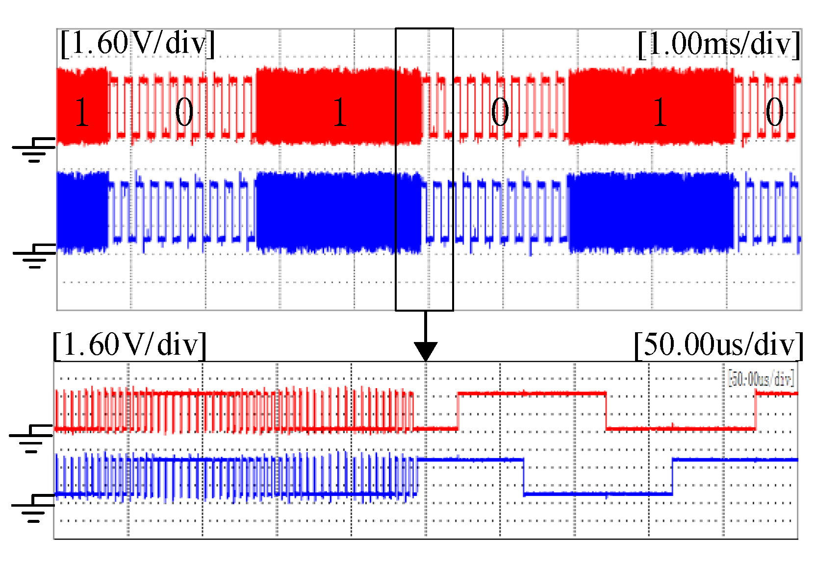
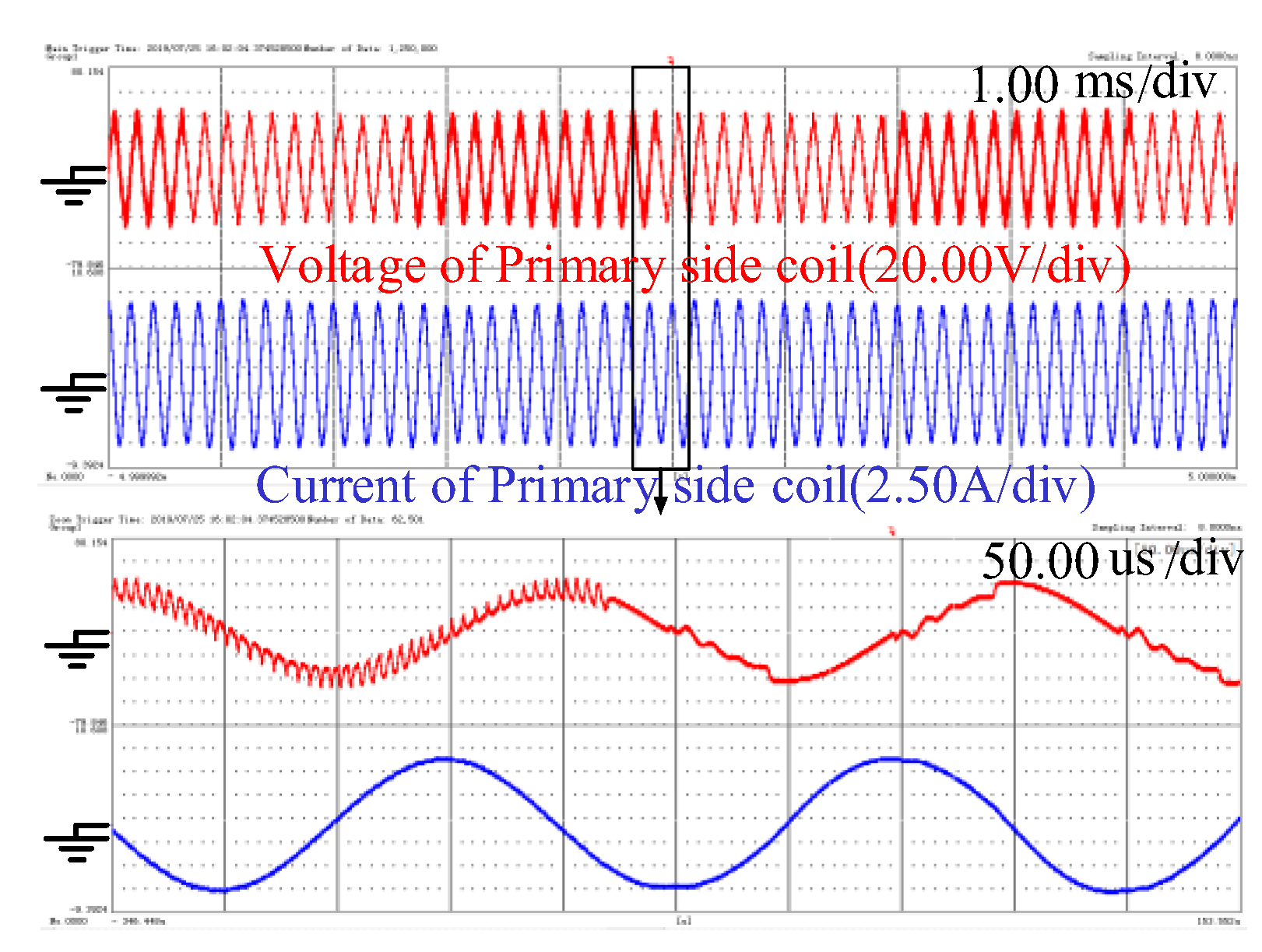
4. Experiment Verification

To verify the feasibility of the proposed structure, an experimental platform was established to analyze the effect of the DFPHM-based SWIPT system. To observe the mutual influence of two frequency waveforms, the voltages of different branches were measured and analyzed. A binary signal transmission experiment in OOK mode was performed to verify the feasibility of information transmission. A GaN-based inverter was designed in this prototype to support the high-frequency signal output, i.e., up to 2 MHz. The EP4CE10 FPGA controller with a 300 MHz system clock was used to generate the control signal. The experiment was observed through a DLM4058 oscilloscope. Figure 9 shows the prototype design, and Table 2 lists the prototype specifications.
Power is transmitted at a frequency of 5 kHz. The frequency of the power transmission is the same as the base frequency of the DFPHM. The 37th harmonic frequency of 5 kHz is 185 kHz, which is used to transmit information. The voltage of the DC source is 7V. Both of the voltage amplitudes of the waveforms at 5 kHz and 185 kHz are set to 5.6V. The first-quarter cycle switching angle of the DFPHM when the inverter outputs dual frequency waveforms is shown in Table 3. When the controller is running in DFPHM mode with the switching angle shown in Table 3, the system transmits dual-frequency signals, and the digital 1 is demodulated on the secondary side. When the system transmits a single frequency signal, the digital 0 is demodulated on the secondary side.
The FPGA controller generates four control signals to control the inverter. The GaN-based full-bridge inverter is controlled by the DFPHM signals, as shown in Figure 10. The different colored waveforms represent the control signals of the four GaN MOSFETs. As shown in the waveform generation process in Figure 3, the control signals of S1 and S4, and of S2 and S3, are synchronized.
Figure 11 shows the output voltage waveform and FFT analysis modulated by DFPHM of the GaN-based full-bridge inverter. Within measured range, the output waveform contains two components. The amplitude of both output frequency voltages is 4V. The waveform is decomposed into two components at 5 kHz and 185 kHz. No harmonics at other frequencies are detected between the two frequencies. Therefore, the full-bridge inverter based on the DFPHM method is capable of generating a dual-frequency signal.
On the secondary side, under the effect of wave trappers and resonance networks, the dual-frequency superimposed signal is demodulated in two branches at different frequencies. The effect of frequency separation was tested experimentally.
The voltage of the low-frequency resonant capacitor on the secondary side is shown in Figure 12. The observed frequency in the Fourier analysis is 5 kHz, but another harmonic frequency, i.e., 185 kHz, is negligible in strength. The dual frequency signal received by the coil is separated into two signals at 5 kHz and 185 kHz. The WT3 limits the 185 kHz signal on the low-frequency branch.
The voltage of the resonant capacitor and its FFT analysis in the 185 kHz branch are shown in Figure 13. The amplitude of the 185 kHz signal is 4.132 V, which can be picked up by the demodulation module. The signal is detected by the demodulation module, where the information is picked up from 185 kHz waveform by using OOK method.
The effect of information transmission and demodulation in OOK mode was tested in the experiments. As shown in Figure 14, the DF-inverter runs in joint operation mode, i.e., the inverter alternates between DFPHM and single frequency mode, which are marked as 1 and 0 in the figure, respectively. The red and blue waveforms represent a set of control signals that drive the inverter.
With the resonant networks, the superimposed sine wave is transferred through loose coils from the primary side to the secondary side. In Figure 15, the red line and the blue line are the voltage and the current of the primary side coil, respectively. According to Figure 15, when transmitting digital 1, the voltage of the secondary side coil is the sine wave with a high frequency harmonic. When transmitting digital 0, the voltage waveform of the secondary side coil only contains a frequency of 5 kHz.
In OOK mode, the signal received by the power load should be undistorted. At the secondary side, R A is the power load, and its voltage and current waveforms are sine waves at 5 kHz, as shown in Figure 16a, where the voltage of R A is red and the current is blue. A Fourier analysis of the voltage waveform shows that the Total Harmonic Distortion (THD) of the power load voltage is 1.66%, as shown in Figure 16b. Power transmission is not affected by information transmission.
In OOK mode, with the inverter’s alternative switching between single-frequency and dual-frequency modes, the digital 0 and 1 are transferred from the primary side to the secondary side, as shown in Figure 17. The green waveform is the current input to the demodulation module. The blue waveform is the voltage that passes through the band-pass filter after being input to the demodulation module. The red waveform is the binary output signal after the signal passes through the amplifier and the comparator. When transmitting digital 0, the demodulation module cannot capture the high-frequency signal amplitude. At this time, the output voltage of the demodulation module is 0V, which represents data 0. When transmitting digital 1, the inverter works in DFPHM mode, and the demodulation module detects the voltage of the high frequency and the output 5V DC voltage. Therefore, the information waveform is converted into binary data on the secondary side.
According to the experiment, the proposed structure can simultaneously transfer information and power via a common inductive link, and demodulate them in two branches on the secondary. No mutual interference occurs between the power transmission and information transmission channels.

5. Conclusions and Future Work

In order to solve the problem of information transmission affecting power transmission in SWIPT systems, this paper proposes a dual-frequency SWIPT structure using the DFPHM control method. In this system, continuous power transmission is not affected by information transmission. This dual-frequency structure contains only one inverter. Power and information are transmitted through a common resonance link and picked up in different branches. This structure reduces the system complexity of dual-frequency SWIPT systems. The wave trappers also reduce the influence of information transmission on power transmission. The experimental results prove the feasibility of the proposed SWIPT system.
The combination of parameters such as the resonant inductance, resonant capacitance, inductance, and capacitance of the wave trappers has an important effect on the separation of the two frequencies in their respective channels. In the future, the influence of the system parameters on dual-frequency transmission performance will be an important issue; optimizing these parameters will allow the system to achieve better performance.

Author Contributions

Conceptualization, J.W.; methodology, J.W. and V.S.; software, P.G. and Z.D.; validation, H.Z., P.G., and Z.D.; formal analysis, J.W.; investigation, J.W. and N.J.; resources, N.J.; writing—original draft preparation, H.Z.; writing—review and editing, J.W. and N.J.; visualization, V.S.; supervision, N.J.; project administration, J.W. and N.J.; funding acquisition, N.J. All authors have read and agreed to the published version of the manuscript.

Funding

This work was supported in part by the National Natural Science Foundation of China under the grant U1604136 and by the Scientific and Technological Program of Henan Province under the grant 202102210090.

Conflicts of Interest

The authors declare no conflict of interest.

References

  1. Krikidis, I.; Timotheou, S.; Nikolaou, S.; Zheng, G.; Ng, D.W.K.; Schober, R. Simultaneous wireless information and power transfer in modern communication systems. IEEE Commun. Mag. 2014, 52, 104–110. [Google Scholar] [CrossRef] [Green Version]
  2. Zhou, X.; Zhang, R.; Ho, C.K. Wireless Information and Power Transfer: Architecture Design and Rate-Energy Tradeoff. IEEE Trans. Commun. 2013, 61, 4754–4767. [Google Scholar] [CrossRef] [Green Version]
  3. Chau, K.T. Electric Vehicle Machines and Drives – Design, Analysis and Application; John Wiley & Sons: Hoboken, NJ, USA, 2015. [Google Scholar]
  4. Zhang, H.; Gao, S.; Ngo, T.; Wu, W.; Guo, Y. Wireless Power Transfer Antenna Alignment Using Intermodulation for Two-Tone Powered Implantable Medical Devices. IEEE Trans. Microw. Theory Tech. 2019, 67, 1708–1716. [Google Scholar] [CrossRef]
  5. Nie, Z.; Yang, Y. A Model Independent Scheme of Adaptive Focusing for Wireless Powering to In-Body Shifting Medical Device. IEEE Trans. Antennas Propag. 2018, 66, 1497–1506. [Google Scholar] [CrossRef]
  6. Zhang, K.; Zhu, Z.; Song, B.; Xu, D. A Power Distribution Model of Magnetic Resonance WPT System in Seawater. In Proceedings of the IEEE 2nd Annual Southern Power Electronics Conference SPEC, Auckland, New Zealand, 5–8 December 2016; pp. 1–4. [Google Scholar]
  7. Hasaba, R.; Okamoto, K.; Kawata, S.; Eguchi, K.; Koyanagi, Y. Experimental Study on Over 10 Meters Magnetic Resonance Wireless Power Transfer under Sea with Coils. In Proceedings of the 2018 IEEE Wireless Power Transfer Conference (WPTC), Montreal, BC, Canada, 3–7 June 2018; pp. 1–4. [Google Scholar]
  8. Si, Y.; Lao, J.; Zhang, X.; Liu, Y.; Cai, S.; González-Vila, Á.; Li, K.; Huang, Y.; Yuan, Y.; Caucheteur, C.; et al. Electrochemical Plasmonic Fiber-optic Sensors for Ultra-Sensitive Heavy Metal Detection. J. Lightwave Technol. 2019, 37, 3495–3502. [Google Scholar] [CrossRef]
  9. Injeti, S.K.; Thunuguntla, V.K. Optimal integration of DGs into radial distribution network in the presence of plug-in electric vehicles to minimize daily active power losses and to improve the voltage profile of the system using bioinspired optimization algorithms. Prot. Control Mod. Power Syst. 2020, 5, 21–35. [Google Scholar] [CrossRef] [Green Version]
  10. Ponnimbaduge Perera, T.D.; Jayakody, D.N.K.; Sharma, S.K.; Chatzinotas, S.; Li, J. Simultaneous Wireless Information and Power Transfer (SWIPT): Recent Advances and Future Challenges. IEEE Commun. Surv. Tutor. 2018, 20, 264–302. [Google Scholar] [CrossRef] [Green Version]
  11. Wang, T.; Liu, X.; Jin, N.; Tang, H.; Yang, X.; Ali, M. Wireless Power Transfer for Battery Powering System. Electronics 2018, 7, 178. [Google Scholar] [CrossRef] [Green Version]
  12. Simard, G.; Sawan, M.; Massicotte, D. High-speed OQPSK and efficient power transfer through inductive link for biomedical implants. IEEE Trans. Biomed. Circuits Syst. 2010, 4, 192–200. [Google Scholar] [CrossRef] [PubMed]
  13. Kim, J.; Wei, G.; Kim, M.; Ryo, H.; Zhu, C. A Wireless Power and Information Simultaneous Transfer Technology Based on 2FSK Modulation Using the Dual Bands of Series–Parallel Combined Resonant Circuit. IEEE Trans. Power Electron. 2019, 34, 2956–2965. [Google Scholar] [CrossRef]
  14. Wu, J.; Zhao, C.Y.; Jin, N.; He, S.B.; Ma, D.G. Bidirectional Information Transmission in SWIPT System with Single Controlled Chopper Receiver. Electronics 2019, 8, 1027. [Google Scholar] [CrossRef] [Green Version]
  15. Wu, J.; Zhao, C.W.; Lin, Z.; Du, J.; Hu, Y.; He, X. Wireless Power and Data Transfer via a Common Inductive Link Using Frequency Division Multiplexing. IEEE Trans. Ind. Electron. 2015, 62, 7810–7820. [Google Scholar] [CrossRef] [Green Version]
  16. Sun, Y.; Yan, P.X.; Wang, Z.H. The parallel transmission of power and data with the shared channel for an inductive power transfer system. IEEE Trans. Power Electron. 2016, 31, 5495–5502. [Google Scholar] [CrossRef]
  17. Pantic, Z.; Lee, K.; Lukic, S.M. Multi-frequency inductive power transfer. IEEE Trans. Power Electron. 2014, 29, 5995–6005. [Google Scholar] [CrossRef]
  18. Liu, W.; Chau, K.T.; Lee, C.H.T.; Jiang, C.; Han, W.; Lam, W.H. Multi-Frequency Multi-Power One-to-Many Wireless Power Transfer System. IEEE Trans. Magn. 2019, 55, 1–9. [Google Scholar] [CrossRef]
  19. Wu, J.; Li, Y.G.; Jin, N.; Deng, W.; Tang, H.J.; Vaclav, S. A GaN-based Wireless Power and Information Transmission Method Using Dual-Frequency Programmed Harmonic Modulation. IEEE Acess 2019, 8, 49848. [Google Scholar] [CrossRef]
  20. Wu, J.; Bie, L.Z.; Jin, N.; Guo, L.L.; Zhang, J.T.; Tao, J.G.; Vaclav, S. Dual-Frequency Output of Wireless Power Transfer System with Single Inverter Using Improved Differential Evolution Algorithm. Energies 2020, 13, 2209. [Google Scholar] [CrossRef]
  21. Sanchez, A.D.R.; Hurtado, J.C.C. Spectral Analysis of OOK modulation with rectangular carrier and it conversion in a signal modulated in OOK with sine carrier. Application in RFID systems. IEEE Lat. Am. Trans. 2016, 14, 2152–2156. [Google Scholar] [CrossRef]
  22. Jeong, D.; Lee, H.; Chung, T.; Lee, S.; Lee, J.; Kim, B. Optimized Ultralow-Power Amplifier for OOK Transmitter With Shaped Voltage Drive. IEEE Trans. Microw. Theory Tech. 2016, 64, 2615. [Google Scholar] [CrossRef]
Figure 1. System circuit diagram of SWIPT system based on DFPHM.
Sustainability 12 04189 g001
Figure 2. Block diagram of transmission process of SWIPT system based on DFPHM.
Sustainability 12 04189 g002
Figure 3. Structure diagram of the dual-frequency inverter.
Sustainability 12 04189 g003
Figure 4. Switching angles of DFPHM control wave.
Sustainability 12 04189 g004
Figure 5. Schematic diagram of control signal encoded in OOK modulation.
Sustainability 12 04189 g005
Figure 6. Circuit diagram of data demodulation module.
Sustainability 12 04189 g006
Figure 7. System equivalent circuit.
Sustainability 12 04189 g007
Figure 8. Bode diagram of wave trapper impedance. (a) Impedance of WT 1 . (b) Impedance of WT 2 .
Sustainability 12 04189 g008
Figure 9. The Prototype of the SWIPT with DFPHM. An FPGA controller is used to drive a GaN inverter.
Sustainability 12 04189 g009
Figure 10. Four control signals output from FPGA.
Sustainability 12 04189 g010
Figure 11. Voltage waveform and FFT analysis modulated by DFPHM of full-bridge output.
Sustainability 12 04189 g011
Figure 12. Voltage and FFT analysis of capacitor at 5 kHz during dual-frequency operation.
Sustainability 12 04189 g012
Figure 13. Voltage and FFT analysis of capacitor at 185 kHz during dual-frequency operation.
Sustainability 12 04189 g013
Figure 14. Control signal waveform when data is encoded in OOK.
Sustainability 12 04189 g014
Figure 15. Waves of the primary side coil while 0 to 1 shifting.
Sustainability 12 04189 g015
Figure 16. Waveforms of the power load R A with DFPHM and Fourier analysis. (a) Voltage and current waves of R A . (b) Fourier Analysis of R A voltage.
Sustainability 12 04189 g016
Figure 17. Demodulation module voltage waveform in OOK mode.
Sustainability 12 04189 g017
Table 1. Frequency Setting of Resonance Branches and Wave Trappers.
BranchPass FrequencyWave TrapperCut-off Frequency
L p ( L s ) with C p a ( C s a ) and WT 1 ( WT 3 ) ω a WT 1 ( WT 3 ) ω b
L p ( L s ) with C p b ( C s b ) and WT 2 ( WT 4 ) ω b WT 2 ( WT 4 ) ω a
Table 2. Parameters of Experiment Platform.
ItemParameterItemParameter
FPGA ControllerEP4CE10 L k p b 2.4 mH
GaN DevicesGS66516T C k s b 87 nF
L p , L s 180 uH L k s b 11.6 mH
M 57.60 uH R A 5 Ω
C p a , C s a 5.4 uF R B 60 Ω
C p b , C s b 4 nFDC Input7 V
C k p a , C k s a 80 nFCoil’s Distance10 cm
C k p b 0.448 uFMaximum Instantaneous Power30 W
L k p a ,   L k s a 9.36 uH
Table 3. First Quarter Cycle Conduction Angle Calculated.
θ 1 = 0.0803 θ 2 = 0.1508 θ 3 = 0.2398 θ 4 = 0.2997 θ 5 = 0.3947
θ 6 = 0.4437 θ 7 = 0.5405 θ 8 = 0.5797 θ 9 = 0.6786 θ 10 = 0.7118
θ 11 = 0.8219 θ 12 = 0.8518 θ 13 = 0.9766 θ 14 = 1.0027 θ 15 = 1.1394
θ 16 = 1.1615 θ 17 = 1.3069 θ 18 = 1.3259 θ 19 = 1.4769 θ 20 = 1.4942

