Article

Study on the Availability of 4T-APS as a Video Monitor and Radiation Detector in Nuclear Accidents

1
School of Environmental and safety engineering, University of South China, Hengyang 421001, China
2
Department of Engineering Physics, Tsinghua University, Beijing 100084, China
3
China Institute of Atomic Energy, Beijing 102413, China
*
Author to whom correspondence should be addressed.
Sustainability 2018, 10(7), 2172; https://doi.org/10.3390/su10072172
Submission received: 9 May 2018 / Revised: 21 June 2018 / Accepted: 22 June 2018 / Published: 26 June 2018
(This article belongs to the Special Issue Nuclear Safety, Emergency, Security: Theory and Technology)

Abstract

:
In this paper, we present the availability of an active pixel sensor (APS) with four transistors (4T) as a video monitor and radiation detector. Analyzing radiation damage must be one of the first steps in recovering from nuclear accidents, and the radiation response characteristic is the basis for the use of 4T-APS to detect radiation. The goal of this work is to suggest the use of cameras with 4T-APS in widely distributed irradiation detectors. The total ionizing dose (TID) of radiation damage on 4T-APS provided a threshold. Radiation tolerance was improved with the help of a radiation shielding structure. The radiation response showed integration time dependence and pixel information dependence, and greater radiation response was observed from the pixels with lower grayscale values. Two methods are suggested based on different monitoring scenes. This study can help to greatly improve nuclear accident emergency response and the safety of nuclear facilities.

1. Introduction

The nuclear accident in Fukushima raised public awareness of ionizing radiation and nuclear accident response activity. This has led to the desire for nuclear countries to improve video monitoring and radiation detection at nuclear facilities. In response, we need to discuss the availability of cameras at radiation accident sites. Video monitoring and radiation detection rely on the pixel sensors of cameras. Complementary metal oxide semiconductor (CMOS) integrated circuits with active pixel sensor (APS) arrays are widely used in cameras, and usually have very low cost, consume little power, have strong environmental adaptability, and are sensitive to radiation. An APS with four transistors (4T) has better background noise and a faster shutter speed than an APS with three transistors. Moreover, because of the separation of the space charge region (SCR) away from the oxide, its radiation resistance is greater than both APS with three transistors and charge coupled device (CCD) pixel sensors [1,2,3,4]. The photodiode in the core of each CMOS 4T-APS is a pinned photodiode (PPD), which is used in more than 99% of APSs today [5] and is designed to detect visible light photons, but is intrinsically sensitive to gamma photons as well. The use of CMOS 4T-APS brings several important advantages with respect to integrated circuits designed ad hoc specifically for application around nuclear facilities. Cameras used in this work cost less than 300 CNY, which would allow a large number of sensors to be arranged at low cost. The widespread distribution of sensors allows integration at an affordable price and with a fast response of detector arrays, such as building a network of arrays for video monitoring and radiation detection. The grayscale value of a pixel was used to measure the strength of the output signal within the range 0 to 2n, where n is the bit depth of Analog-to-Digital Converter (ADC) resolution, and the unit of the grayscale value is “gray”.
This work presents a study on the availability of 4T-APS as a monitor and detector in nuclear accidents. As a video monitor, we were mainly concerned about performance deterioration and damage of a 4T-APS at a nuclear accident site. According to the results of early theoretical research, the main radiation damage that degrades APS performance is the generation of defects in the oxides of the pinned photodiodes, such as positive-trapped charges and interface states, which lead to an increase in dark current [6,7]. In order to understand the radiation damage of 4T-APSs used at nuclear radiation accidents, we must improve our understanding of the damage induced by the total ionizing dose (TID), with the aim of studying the availability of 4T-APSs by testing their radiation resistance. In recent years, research on the application of smartphone cameras for radiation detection has been popular, and study results have proved that smartphone APSs can be used for gamma photon detection [8,9]. Based on the radiation response effect between CMOS APS and gamma photons, the possibility of using CMOS APS to directly detect radiation has been confirmed [10]. The response effect is also related to the particle type (such as gamma photon, electron, neutron, etc.) and energy [11,12,13,14]. This radiation response characteristic enables APS to be used as monitoring and radiation alarm equipment under the conditions of a nuclear accident [15]. However, the radiation response of APS under visible light and at different integration times is rarely reported. Therefore, the understanding of radiation detection of 4T-APSs should be improved by testing their radiation response characteristics at different integration times and with different pixel information. The pixel information is related to the signal values of pixels in different regions of the sensor area before irradiation.
In this work, the possibilities, limitations, and improvements of such sensors are discussed. A statistical study was executed in order to underline the grayscale value increase under different irradiation dose rates. The paper is organized as follows: Experimental setup and data-processing methods are detailed in Section 2. Results and discussion are described in Section 3. In Section 4, we discuss the applications and improvements of 4T-APS as a monitor and detector at nuclear accidents. Our conclusions are presented in Section 5.

2. Materials and Methods

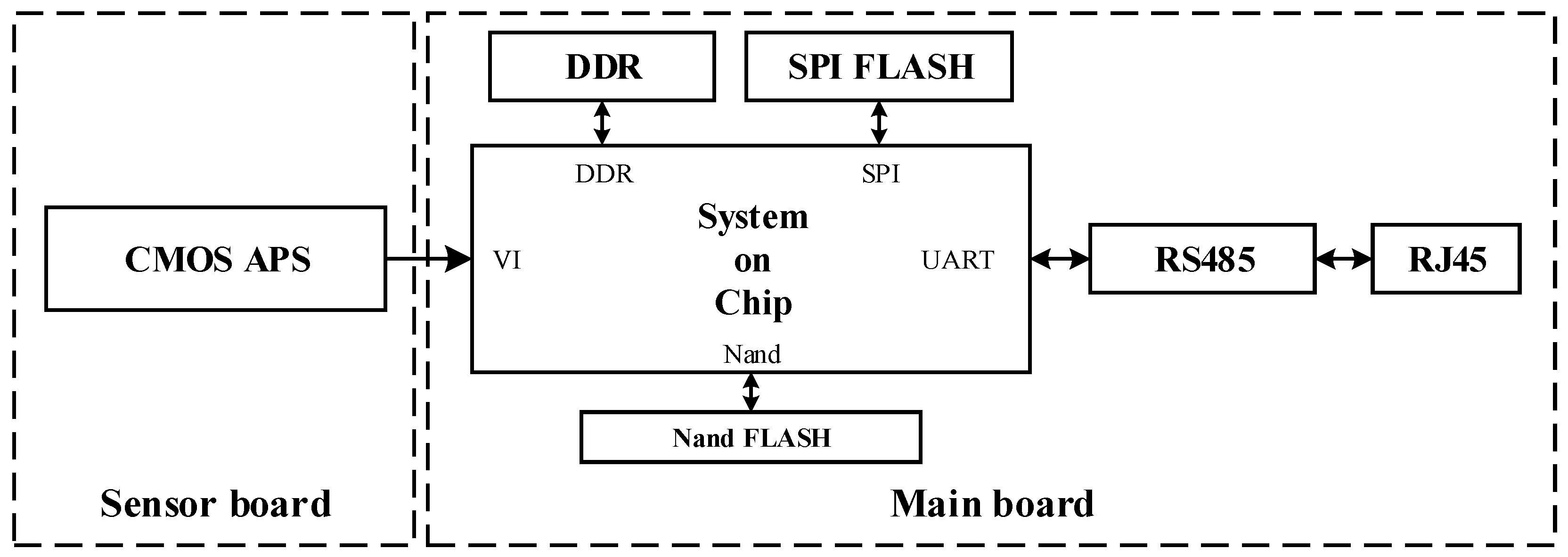
2.1. Experimental Setup

This study used a set of cameras equipped with a 6.4 mm (type 1/2.8) CMOS active pixel-type commercial image sensor, made of a square pixel array and approximately 2.43 M effective pixels. Sensors were manufactured in a commercially available 0.18 μm process and the pixel pitch was 2.8 μm. The bit depth of the sensors was 8. The chips operated with analog 2.7 V, digital 1.2 V, and interface 1.8 V triple power supplies. The red (R), green (G), and blue (B) primary color pigment mosaic filters were adopted in these sensors. The cameras were comprised of an image-processing circuit, the Ambarella A5S ARM11, which provided a video signal that was captured using a HikVision (Hangzhou, Zhejiang, China) model DS-7804N-K1/C network video recorder (NVR) that digitalizes the signal using 8 bits.
Figure 1 shows a structural diagram of the camera used in this work. Chips were integrated on two printed circuit boards, the sensor board and the main board. The CMOS APS and peripheral circuits were integrated on the sensor board, whose function was signal acquisition. On the main board, the system-on-chip device was responsible for readout signals from sensor board and digital signal processing. The transmission module formed by RS485 and RJ45 was also integrated on the main board. Data transmission and power supply were achieved with the help of a flexible print circuit between the two boards. If any board (sensor or main board) is broken down during irradiation, a new one can replace it to keep the camera operational.
The camera samples were exposed to a columnar 60Co γ-ray radioactive source with photon energies of 1.17 and 1.33 MeV. The activity of the radioactive source was 90 kCi. Figure 2 illustrates the experimental setup that was used to test the radiation damage and radiation response of the cameras. A silver dichromate chemical dosimeter was used to measure radiation exposure at the cameras’ locations. The 60Co γ-ray source, cameras, switch, and direct current (DC) power were placed in the radiation area. A network video recorder, personal computer (PC), and further power supply were located in the operation area; without any irradiation. Signal data was transmitted by using a 4800LX cable. During experiments, cameras were placed at different points along the path of sample placement. The irradiation dose rate ranged from 5.24 to 1782 Gy/h. All of the samples were in operation throughout the experiment. Cameras were placed in an opaque experimental box with a video test card. The box helped insulate the samples and detectors from the visible light from outside. A test card, a page of colorful paper in front of the camera lens, was used to provide pixel information in the video frames. When we studied the radiation response of the APS at different pixel information regions in frames, a stable light source was used to help the cameras acquire video information on the test card. The color temperature of the stable light source in the box was 6000 K, and the mean illumination was 3744 lux.

2.2. Data-Processing Methods

Recorded videos were processed on a PC running video-editing software, which was used to select the videos recorded during and after irradiation. Each video was converted into individual frames (25 fps according to the sampling rate; each frame being an independent image) with the help of data-processing software, and each frame series was saved in the JPEG file format. Due to the 8-bit depth of the ADC resolution, the range of pixel grayscale values is from 0 to 255 and the unit is the “gray”.
The mean grayscale value (Dk) of the selected images at the radiation dose rate of k was calculated as follows:
D k = 1 M N j = 1 j = M i = 1 i = N E i , j ,
where Ei,j is the grayscale value of the ith pixel in the jth frame at the radiation dose rate k, M is the number of frames, and N is the pixel count.
The total grayscale incremental value (Sk) at the radiation dose rate k was calculated as follows:
S k = j = 1 j = M i = 1 i = N ( E i , j I i , j )
where Ii,j is the grayscale value of the ith pixel in the jth frame before irradiation.

3. Results and Analysis

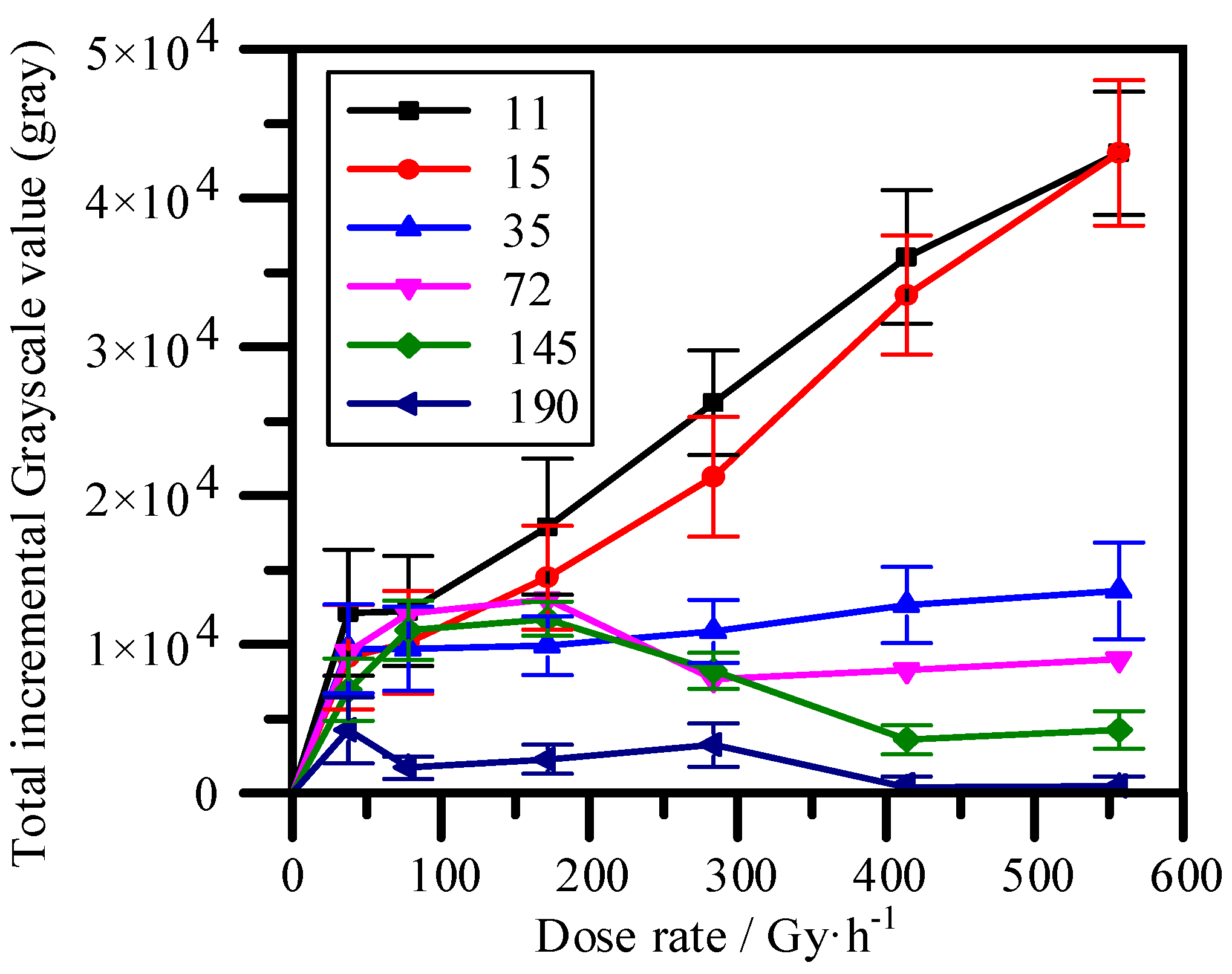
3.1. Radiation Damage

In this section, we describe the operation lifetime and noise increase of sensors after γ-ray irradiation. Table 1 shows the experimental conditions of irradiation and operation lifetime of the sensors. Five different dose rates were used in this experiment. The operation lifetime represents the total operation time of each board before it is dead under that dose of irradiation, and the “Dose” in Table 1 is the irradiation dose when the board broke down. As we can see from Table 1, the range of radiation tolerance of main boards is between 165.58 Gy and 274.08 Gy; the difference is more than 100 Gy. The radiation tolerance of the sensor board can also be seen in Table 1. Compared with the main board, the sensor board had a much stronger radiation tolerance and a smaller difference of TID; the TID of all the sensor boards was above 490 Gy. Combined with the structural introduction from Figure 1, data-processing devices, data-transmission devices, and other peripheral circuits with special functions are integrated on the main board, but the only radiation-sensitive device on the sensor board is the 4T-APS. Therefore, the random radiation damage effects on the electronic devices caused different operation lifetimes between the boards, and the operation lifetime result could therefore represent the lifetime of the 4T-APS.
As we know from Reference [7], the dark current increases with larger TID and leads to increased noise. In order to improve our understanding of the total ionizing dose effect from induced radiation damage, we need to study the noise increment of the 4T-APS before the sensor board dies. Figure 3 shows the mean grayscale value of the 4T-APS versus the TID. All of the samples were running throughout the experiment, and the video data was recorded under non-irradiation conditions after nine different TID irradiations. As we can see from Figure 3, the mean grayscale value increases with larger TID, but an obvious threshold can observed from the curve. When the TID is lower than 38 Gy, there is no significant change in mean grayscale value. However, when the TID is higher than 40 Gy, the mean grayscale value increases.
The existence of the TID threshold can be explained by the analysis results shown in Figure 4, which shows the cross-sectional view of the space charge region of the 4T-APS after different TID irradiations. Ionizing irradiation causes an increase in the density of oxide-traps and interface-traps, which induced an increase in the dark current generation rate. Meanwhile, with the increase of the two types of traps, the space charge region (SCR) spreads to the oxide layer and shallow trench isolation (STI), and the diffusion current contribution in the SCR is larger than the originating volume [16]. Therefore, the dark current increases with larger contact area between the SCR and STI, and is shown by the grayscale value of pixels without exposure to light and irradiation. The space charge region does not spread to touch the oxide layer and STI at lower TID, so the increased grayscale value of pixels caused by the dark current increase with TID is very small. However, with TID increase, SCR can touch the oxide layer and STI, in which case the traps caused by TID are rich [17]. The pixel grayscale value increases sharply with larger contact area between the SCR and STI. This can explain why the curve in Figure 3 is flat before 38 Gy and increases sharply after 40 Gy.
We can conclude that for the 4T-APS, no radiation-hardening and data-processing are needed before TID reaches the radiation damage threshold. In order to exclude the radiation damage effects during the radiation response study, the TIDs of all the sensors were kept less than 38 Gy in the following radiation response experiments.

3.2. Radiation Response

The number of APSs giving a radiation response signal is a measure for the amount of gamma photons hitting the camera pixels. Charges generated in the hit pixel lead to an increased grayscale value. We can study the radiation response of the APS with help of Equations (1) and (2). Figure 5 shows the mean grayscale value as a function of irradiation dose rate. All of the video data were recorded under 16 irradiation dose rates from 8 to 276 Gy/h, and the dose was changed by varying the distance between the radiation 60Co source and the sensor holder position along with the path of sample placement, as shown in Figure 2. The TIDs of all the irradiated sensors were less than 20 Gy to reduce interference from the radiation damage effects, discussed above. The integration time was set as 1/25 s. The sensors were shaded to insulate from visible light. As shown in Figure 5, the mean grayscale value of sensors increases linearly with increased dose rates from 5.24 Gy/h to 69.24 Gy/h; after 70 Gy/h, the radiation response of the 4T-APS gradually reaches saturation. When the irradiation dose is larger than 155 Gy/h, the curve shows no relationship between dose rate and mean grayscale value.
Figure 6 shows the mean grayscale value as a function of the irradiation dose rate at eight integration times, ranging from 1/10,000 s to 1/100 s. An increase in grayscale value with increased irradiation is shown in the figure. The curve in Figure 5 has a much steeper initial gradient and saturates at the same level as those in Figure 6. The value recorded by the sensors for a longer integration time was greater than that for a shorter integration time with the same dose of irradiation. Additionally, the linear range of the curves in Figure 6 with the shorter integration time is shorter. The curve at 1/8000 s is similar to the curve at 1/10,000 s. This is probably due to two reasons: (1) the minimum extremum of the integration time was 1/8000; (2) changing the integration time shorter than 1/8000 has little effect on the collection of radiation-induced charges.
When the originating neutral volume of the SCR is small and unchanged before irradiation, the TID reaches the threshold, thus we ignore the radiation damage effects and the integration time limits the ability of the SCR to collect radiation-induced charges. When the integration time is 1/25 s, we find linear radiation response from 5 to 70 Gy/h, but if we need to use the same 4T-APS to detect higher dose rates above 70 Gy/h, we needed to decrease the integration time. A good linear radiation response range from 70 to 100 Gy/h can be obtained at the integration time of 1/100 s. Furthermore, 1/240 s is applicable to dose rates from 100 to 550 Gy/h; 1/480 s is applicable to dose rates from 550 to 1000 Gy/h; and 1/1000 s is applicable to dose rates from 1000 to 1300 Gy/h.
Figure 7 shows the relationship between the mean grayscale value and irradiation dose at different grayscale pixel regions in the imaging frames. Radiation damage can be ignored because the irradiation TIDs were less than 20 Gy, and the integration time was set to 1/240 s. During the experiment, the sensors were placed in an opaque experimental box with a video test card and a stable light source. As we can see from Figure 7, curves with initial average greyscale values of 11 and 15 (gray) have better linearity at irradiation dose rates from 38 to 557 Gy/h, but an unobvious relationship between the incremental grayscale value and the irradiation dose rate is observed in the regions with grayscale greater than 35. Results indicate that the frames with higher grayscale values show an irregular radiation response.

4. Discussion and Application

4.1. Video Monitoring

As we learned from the results of the radiation damage experiment, a threshold exists in radiation damage effects. Under lower TID, the inherent radiation resistance of the sensors could withstand radiation damage in a short time. However, the grayscale value of pixels increased sharply when the TID exceeded the threshold. The growth curve did not always have the same slope. In this paper, no obvious change was seen before 38 Gy and the trend of increasing value slowed down after 63.58 Gy. Therefore, cameras with 4T-APS could be available in a nuclear accident with strong radiation for a short time; when the effects of radiation damage can be ignored.
Radiation hardening is an effective method to improve the radiation tolerance of cameras. Radiation shielding could be easy to include on cameras with the structure described in this paper. We can use shielding materials to shield against front incident and scattered γ-rays. A 3D diagram of a radiation hardening shielding structure is shown in Figure 8. Two containers are used to protect the devices on the boards and maintain their stability. Shielding layers made of heavy metals such as tungsten and lead are used to shield γ-rays. Two holes are set to enable the 4T-APS to receive visible light and connect the transmission line with the main board. Fixed frames are used to fix the shielding structure. We can also add other transparent shielding materials in front of the translucent hole to reduce the radiation of the frontal γ-rays. The light transmittance of transparent shielding materials is easily decreased by radiation damage [18], and weakens the radiation response of the 4T-APS to γ-rays. The optimal shielding design is to make the sensor board and the main board have the same operation lifetime; the middle shielding layer is the key in this radiation hardening shielding structure.

4.2. Radiation Detection

Using cameras as γ-ray radiation detectors can be done by analyzing the radiation response characteristics of 4T-APS. According to the experimental results on the integration time dependence and pixel information dependence, the radiation response signals in dark images were proportional to the radiation dose rate and integration time. The lower the grayscale value of pixels, the more obvious the response degree was. Therefore, we propose two methods to use 4T-APS to detect radiation during video monitoring: (1) use a specific 4T-APS device as a dose rate detector, which is dark folded to cut off visible light; and (2) analyze the output signal data from pixels with a grayscale value below 15 (gray). The first method can approach higher detection efficiency and accuracy, but an extra processed 4T-APS device has to be added in the camera system. This detector could be calibrated by recording the corresponding relationship between the response signal and the radiation dose rate at every integration time. The second method can realize video monitoring and radiation detection simultaneously, but this method is ineffective when the scene of the monitored image moves fast. The camera could be calibrated by recording the corresponding relationship between the response signal in the pixel regions with gray value below 15 (gray) and irradiation dose rates at every integration time. The detection accuracy and efficiency of the second method are lower than the first method due to the interference of monitoring images. Therefore, the method should be chosen by analyzing the characteristics of the facility and the types of nuclear accident that could occur in nuclear facilities.

5. Conclusions

In this paper, we focused on researching the availability and methods of using a camera with a 4T-APS as both a video monitor and radiation detector. The radiation damage and radiation response of the 4T-APS were discussed by analyzing results from our irradiation experiment. According to the results, the following conclusions can be drawn.
A threshold exists in the radiation damage effect. Radiation damage can be ignored with the help of the inherent radiation resistance of sensors under lower TID, but noise increases with higher TID. For the sensors in this paper, the TID threshold was 38 Gy, and the noise increase slowed down after 63.58 Gy. Radiation tolerance could be improved with the help of a radiation shielding structure.
The radiation response shows the integration time dependence and pixel information dependence. Pixels in regions with gray value below 15 (gray) had greater radiation response capability. This characteristic enables cameras with 4T-APS to be used for radiation detection. Two detection methods are suggested: either higher detection efficiency and accuracy can be achieved by using an extra-processed 4T-APS that is dark-folded to cut off visible light; or both monitoring and detection can be achieved when the camera is used at a fixed scene, and some pixel regions exist with a grayscale value less than 13 in the video monitoring frames.

Author Contributions

Conceptualization: S.X., S.Z., Y.H. and Y.Q. Data curation: S.X. and Y.H. Investigation, S.X. and S.Z. Supervision, S.Z. Writing, S.X.

Funding

This research was funded by the Hunan Provincial Key Laboratory of Emergency Safety Technology and Equipment for Nuclear Facilities and partly by the School of Nuclear Science and Technology of the University of South China. The experiments described here were funded by the Major Science and Technology Projects in the Hunan Province Program (Project No. 2012FJ1007).

Acknowledgments

The authors would like to express their sincere gratitude to the China Institute of Atomic Energy for providing the 60Co γ source and the nuclear radiation detector.

Conflicts of Interest

The authors declare no conflict of interest.

References

  1. Goiffon, V.; Magnan, P.; Saint-Pé, O.; Bernard, F.; Rolland, G. Ionization versus displacement damage effects in proton irradiated CMOS sensors manufactured in deep submicron process. Nucl. Instrum. Methods Phys. Res. 2009, 610, 225–229. [Google Scholar] [CrossRef] [Green Version]
  2. Goiffon, V.; Virmontois, C.; Magnan, P.; Cervantes, P.; Corbière, F.; Estribeau, M.; Pinel, P. Radiation Damages in CMOS Image Sensors: Testing and Hardening Challenges Brought by Deep Sub-Micrometer CIS Processes. In Proceedings of the Sensors, Systems, and Next-Generation Satellites XIV (78261S), Toulouse, France, 13 October 2010. [Google Scholar] [CrossRef] [Green Version]
  3. Xu, S.L.; Zou, S.L.; Wu, Z.; Luo, Z.P.; Huang, Y.J.; Cai, X.M. Comparative Study on Ionizing Radiation Damage of Different Types of Image Sensor Modules. At. Energy Sci. Technol. 2016, 50, 2092–2100. [Google Scholar]
  4. Xu, S.L.; Zou, S.L.; Huang, Y.J. Effect of γ-ray Ionizing Radiation on CMOS Active Pixel Sensor. Chin. J. Lumin. 2017, 38, 308–315. [Google Scholar] [CrossRef]
  5. Fossum, E.R.; Hondongwa, D.B. A review of the pinned photodiode for CCD and CMOS image sensors. IEEE J. Electron Devices Soc. 2014, 2, 33–43. [Google Scholar] [CrossRef]
  6. Bagatin, M.; Gerardin, S. Ionizing Radiation Effects in Electronics: From Memories to Imagers; CRC Press: Boca Raton, FL, USA, 2015; pp. 2720–2722. ISBN 9781498722605. [Google Scholar]
  7. Kang, H.G.; Song, J.J.; Lee, K.; Nam, K.C.; Hong, S.J.; Kim, H.C. An investigation of medical radiation detection using CMOS image sensors in smartphones. Nucl. Instrum. Methods Phys. Res. 2016, 823, 126–134. [Google Scholar] [CrossRef]
  8. Sandy, T. Measurement of Gamma-Rays Using Smartphones. Open J. Appl. Sci. 2016, 6, 31–37. [Google Scholar] [CrossRef]
  9. Goiffon, V.; Estribeau, M.; Cervantes, P.; Molina, R.; Gaillardin, M.; Magnan, P. Influence of transfer gate design and bias on the radiation hardness of pinned photodiode CMOS image sensors. IEEE Trans. Nucl. Sci. 2014, 61, 3290–3301. [Google Scholar] [CrossRef]
  10. Wei, Q.Y.; Wang, Z.P.; Dai, T.T.; Yu, G. Nuclear Radiation Detection Based on Un-covered CMOS Camera under Static Scene. At. Energy Sci. Technol. 2017, 51, 175–179. [Google Scholar] [CrossRef]
  11. Cogliati, J.J.; Derr, K.W.; Wharton, J. Using CMOS Sensors in a Cellphone for Gamma Detection and Classification. arXiv, 2014; arXiv:1401.0766. [Google Scholar]
  12. Pérez, M.; Lipovetzky, J.; Haro, M.S.; Sidelnik, I.; Blostein, J.J.; Bessia, A.; Berisso, M.G. Particle detection and classification using commercial off the shelf CMOS image sensors. Nucl. Instrum. Methods Phys. Res. 2016, 827, 171–180. [Google Scholar] [CrossRef]
  13. Xu, S.L.; Zou, S.L.; Huang, Y.J. γ-ray Detection Using Commercial Off-The-Shelf CMOS and CCD Image Sensors. IEEE Sens. J. 2017, 17, 6599–6604. [Google Scholar] [CrossRef]
  14. Xu, S.L.; Zou, S.L.; Huang, Y.J.; Kuang, Y.; Guo, Z. Analysis of Photon Radiation Response Characteristics of 4T-PPD-APS. Acta Opt. Sin. 2018. Available online: http://kns.cnki.net/kcms/detail/31.1252.O4.20180116.1028.022.html (accessed on 16 January 2018).
  15. Xu, S.L.; Zou, S.L.; Wu, Z.; Song, L. Research on Availability of CIS Digital Module as Monitoring and Radiation Alarm Equipment under Condition of Nuclear Accidents. Nucl. Power Eng. 2017, 38, 88–94. [Google Scholar] [CrossRef]
  16. Goiffon, V.; Virmontois, C.; Magnan, P.; Cervantes, P.; Place, S.; Gaillardin, M.; Girard, S.; Paillet, P.; Estribeau, M.; Martin-Gonthier, P. Identification of Radiation Induced Dark Current Sources in Pinned Photodiode CMOS Image Sensors. IEEE Trans. Nucl. Sci. 2012, 59, 918–926. [Google Scholar] [CrossRef] [Green Version]
  17. Goiffon, V.; Estribeau, M.; Marcelot, O.; Cervantes, P.; Magnan, P.; Gaillardin, M.; Virmontois, C.; Martin-Gonthier, P.; Molina, R.; Corbiere, F.; et al. Radiation Effects in Pinned Photodiode CMOS Image Sensors: Pixel Performance Degradation Due to Total Ionizing Dose. IEEE Trans. Nucl. Sci. 2013, 59, 2878–2887. [Google Scholar] [CrossRef] [Green Version]
  18. Liu, Y.; Zou, S.; Kuang, Y. Effect of γ-ray Radiation and Sun Exposure on Transmittance of ZF6 Lead Glass. At. Energy Sci. Technol. 2016, 49, 2293–2298. [Google Scholar] [CrossRef]
Figure 1. Structural diagram of the camera. CMOS APS, complementary metal oxide semiconductor active pixel sensor; DDR, double data rate synchronous dynamic random access memory; SPI, serial peripheral interface.
Sustainability 10 02172 g001
Figure 2. Schematic diagram showing the experimental setup. NVR, network video recorder; PC, personal computer; DC, direct current.
Sustainability 10 02172 g002
Figure 3. Mean grayscale value as a function of total ionizing dose before the sensor board dies.
Sustainability 10 02172 g003
Figure 4. Cross-sectional view of the four transistor active pixel sensor (4T-APS) after different total ionizing dose (TID) irradiation. PEPI, P type epitaxial; P, P type doped region; P+, P+ type doped region.
Sustainability 10 02172 g004
Figure 5. Mean grayscale value as a function of irradiation dose rate for an integration time of 1/25 s.
Sustainability 10 02172 g005
Figure 6. Mean grayscale value as a function of irradiation dose rate for different integration times. (a) Integration times from 1/1000 s to 1/100 s. (b) Integration times from 1/2000 s to 1/10,000 s.
Sustainability 10 02172 g006
Figure 7. Total incremental grayscale value as a function of irradiation dose rate at different pixel information regions in the imaging frames.
Sustainability 10 02172 g007
Figure 8. 3D diagram of radiation hardening shielding structure.
Sustainability 10 02172 g008
Table 1. Experimental conditions of irradiation and sensor operation lifetime.
No.Board TypeDose Rate (Gy·h–1)Operation Lifetime (h)Dose (Gy)
1Main board104.801.58165.58
2104.801.53160.34
3113.271.68190.29
44550.33150.15
51142.000.24274.08
6Sensor board409.31.22499.35
7409.31.2491.16
811420.45513.90

