Article

Development of a High-Switching-Frequency Motor Controller Based on SiC Discrete Components

State Key Laboratory of High Density Electromagnetic Power and Systems, Institute of Electrical Engineering, Chinese Academy of Sciences, Haidian District, Beijing 100190, China
*
Author to whom correspondence should be addressed.
World Electr. Veh. J. 2025, 16(8), 474; https://doi.org/10.3390/wevj16080474
Submission received: 17 June 2025 / Revised: 1 August 2025 / Accepted: 14 August 2025 / Published: 19 August 2025

Abstract

Discrete Silicon Carbide Metal-Oxide-Semiconductor Field-Effect Transistors (SiC MOSFETs) are characterized by their lower parasitic parameters and single-chip design, enabling them to achieve even faster switching speeds. However, the rapid rate of change in voltage (dv/dt) and current (di/dt) can lead to overshoot and oscillation in both voltage and current, ultimately limiting the performance of high-frequency operations. To address this issue, this paper presents a high-switching-frequency motor controller that utilizes discrete SiC MOSFETs. To achieve a high switching frequency for the controller while minimizing current oscillation and voltage overshoot, a novel electronic system architecture is proposed. Additionally, a passive driving circuit is designed to suppress gate oscillation without the need for additional control circuits. A new printed circuit board (PCB) laminate stack featuring low parasitic inductance, high current conduction capacity, and efficient heat dissipation is also developed using advanced wiring technology and a specialized heat dissipation structure. Compared to traditional methods, the proposed circuit and bus design features a simpler structure, a higher power density, and achieves a 13% reduction in current overshoot, along with a 15.7% decrease in switching loss. The silicon carbide (SiC) controller developed from this research has successfully undergone double-pulse and power testing. The results indicate that the designed controller can operate reliably over extended periods at a switching frequency of 50 kHz, achieving a maximum efficiency of 98.2% and a power density of 9 kW/kg (10 kW/L). The switching frequency and quality density achieved by the controller have not been observed in previous studies. This controller is suitable for use in the development of new energy electrical systems.

1. Introduction

With the rapid development of high-frequency and high-efficiency applications such as aerospace, rail transportation, and underwater propulsion systems, Silicon Carbide Metal-Oxide-Semiconductor Field-Effect Transistors (SiC MOSFETs) have emerged as core components in power electronic systems [1,2,3,4]. Compared to insulated gate bipolar transistors (IGBTs), SiC MOSFETs offer several advantages, including lower switching and conduction losses, higher operating frequencies, superior thermal conductivity, and a higher breakdown electric field [5,6,7]. These characteristics facilitate the miniaturization, lightweight design, and high power density of controllers. However, SiC MOSFET modules face challenges related to complex packaging, parallel current sharing, and reliability requirements, which hinder their ability to fully leverage their high-frequency capabilities. In contrast, silicon carbide MOSFET discrete devices offer low cost, high flexibility, and the capability to achieve smaller sizes and higher switching frequencies due to their minimal parasitic parameters and single-chip design. When current requirements are met, it becomes easier to implement high-frequency and high-power-density controllers. Nevertheless, the rapid switching process renders SiC MOSFETs highly sensitive to stray parameters, which can lead to voltage overshoot and high-frequency oscillations [8]. These issues significantly limit the potential for increasing switching frequency and may adversely affect the normal operation of the devices in severe cases.
Gate circuit control can provide multiple degrees of freedom for managing the switching behavior of SiC MOSFET devices [9]. On the drive side, the switching trajectory can be adjusted and optimized, and several studies have been conducted in this area. To suppress switching overshoot, oscillation, and crosstalk, the most straightforward approach is to increase the gate resistance. While increasing the gate resistance can mitigate overshoot, oscillation, and crosstalk, it also significantly raises switching losses and delays, compromising the high-speed performance of SiC MOSFETs, which exhibit high-frequency characteristics. This is undesirable [10,11]. In recent years, Active Gate Driver (AGD) technology has advanced rapidly due to its high flexibility [12,13,14,15]. AGD can be categorized into different types based on various control variables, such as variable voltage and variable current. Variable voltage AGD provides multiple drive levels during the device switching process, regulates the switching trajectory, and effectively reduces switching losses [16,17]. The greater the number of output levels, the higher the degree of control and the better the performance; however, this also significantly increases the design complexity of the driving circuit, and the isolation power supply requirements also increase substantially [16]. Variable current active gate drive (AGD) suppresses switching overshoot and oscillation by adjusting the drive output current or by adding injected current [18,19,20]. However, the current control circuit reflects a more complex structure and higher costs, and current injection compromises the switching speed and increases the losses of the device while mitigating oscillation and overshoot. In conclusion, active or intelligent gate circuit control methods represent a developmental trend for managing the switching trajectory of silicon carbide (SiC) devices. Nevertheless, the relationship between the controllable target and the control variable in the switch trajectory control method based on active gate driving still lacks model guidance. Additionally, there is a deficiency in collaborative optimization among multiple control targets. Most importantly, these circuits exhibit disadvantages such as high complexity and elevated costs, which hinder the achievement of high power density in driving circuits for high-switching-frequency controllers.
Furthermore, in the design of medium- and high-power controllers, silicon carbide (SiC) power modules are predominantly utilized. Traditional copper metal buses are widely employed in medium- and high-power-level controllers due to their excellent current-carrying capacity, high-temperature resistance, and effective heat dissipation. Currently, a significant amount of literature has investigated the laminated bus structure for SiC power modules [21,22,23]. Reference [21] developed a mother bus structure that integrates printed circuit boards with copper strips. Various stacking methods were analyzed, demonstrating effectiveness in suppressing bus voltage. However, this approach is only applicable to specific packaged modules. Reference [22] adopted an optimization design based on a planar structure, aiming to minimize the parasitic inductance of the busbar. However, this method will increase the switching loss. Reference [23] proposed a design method for vertical busbars, but this method is only applicable to power modules with specific mechanical structures. Unlike power modules, discrete components require printed circuit board (PCB) laminated buses to establish close connections with capacitors and other components, facilitating high integration and lightweight designs. However, PCB laminated buses exhibit relatively high parasitic inductance and capacitance due to the PCB dielectric layer, which can exacerbate oscillations at high frequencies. Additionally, issues such as inadequate current-carrying capacity and poor heat dissipation are prevalent. Currently, there is limited literature on the design of laminated buses in the context of discrete component applications. Reference [24] proposed an optimization design method aimed at reducing the stray inductance of PCB wiring while achieving effective current sharing. Experimental and simulation results demonstrate that this method can effectively suppress the overshoot phenomenon of the turn-off voltage and facilitate current sharing. However, the entire analysis process relies solely on software simulations and does not provide a quantitative analysis of the stray inductance model of the laminated busbar from a mathematical perspective. Additionally, the heat dissipation of the busbar is not considered, which poses a risk of thermal failure.
In conclusion, the key issues that must be addressed in the controller system utilizing discrete SiC MOSFETs for high switching frequencies include the gate oscillation problem, the low parasitic inductance of PCB laminated busbars, the challenge of accommodating large current-carrying capacity, and the need for efficient heat dissipation. This paper presents the design and implementation of a high-switching-frequency motor controller based on discrete SiC MOSFETs. To achieve a high switching frequency while minimizing current oscillation and voltage overshoot, a novel electronic system architecture is proposed. Additionally, a passive driving circuit is designed to suppress gate oscillation. A new PCB laminate stack, featuring low parasitic inductance, high current conduction capacity, and efficient heat dissipation, is developed using advanced wiring technology and a specialized heat dissipation structure. Compared to traditional methods, the proposed driving circuit is both simple and practical. It not only reduces gate oscillation but also decreases switching loss. Additionally, the designed bus method features a unique laminated structure, along with an innovative heat dissipation design. Together, these elements contribute to achieving high power density. The SiC motor controller, developed from these research findings, has undergone double-pulse and power experiments. The results demonstrate that the designed SiC controller can operate reliably over extended periods at a switching frequency of 50 kHz, achieving a maximum efficiency of 98.2% and a power-to-weight ratio of 9 kW/kg, making it suitable for the development of new energy electrification systems.

2. Design of a High-Switching-Frequency Controller Using Discrete SiC MOSFET Devices

2.1. Design of Electrical Architecture for Controllers

The principal block diagram of the main circuit of this control system is illustrated in Figure 1. It employs a typical two-level, three-phase inverter bridge circuit topology. Each phase bridge arm consists of upper and lower transistors, utilizing one TO247-4 packaged discrete SiC MOSFET. In total, the system incorporates six SiC MOSFETs. A compact film capacitor, C1, is connected in parallel on the bus line to enhance power density.
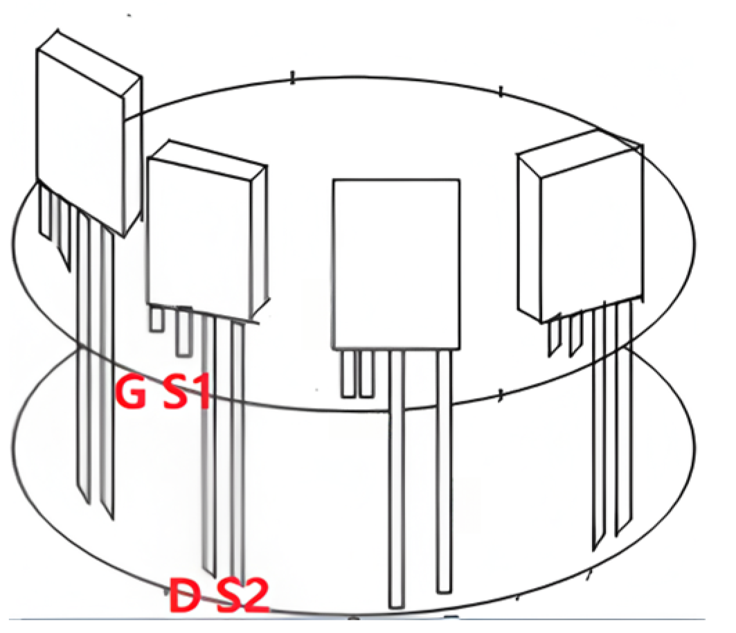
The designed electronic control system consists of three components: the control circuit, the drive circuit, and the power circuit. To minimize the current loop and reduce mutual interference between the power loop and the drive loop, the power board and the drive circuit board are implemented as two separate printed circuit boards (PCBs). The Kelvin pins of the SiC MOSFET effectively isolate the power loop from the drive loop in terms of current. The gate (G) and the Kelvin source pin (S1) are soldered onto the drive board, while the power source pin (S2) and the drain pin (D) are soldered onto the power board. This approach not only prevents high-voltage transient signals from interfering with the gate voltage but also enhances switching speed and reduces switching losses [25]. The control circuit board, drive circuit board, and power circuit board are designed with a three-layer structure. To minimize coupling capacitance and stray inductance in the power loop, a multi-layer PCB structure is employed to create a low-inductance stacked bus. As illustrated in Figure 2, the layout of the designed electronic system not only reduces the overall volume of the motor controller, thereby improving its integration and power density, but also achieves cost savings.
To maximize the utilization of materials and space while addressing electrical and thermal dissipation, the entire system was designed collaboratively, incorporating the power module, drive circuit, capacitors, and busbar. The supporting capacitors on the DC side consisted of multiple single capacitors connected in parallel and soldered onto the power board. These capacitors were linked to the corresponding pins of each parallel power module through a copper layer, effectively reducing equivalent series inductance (ESL) and equivalent series resistance (ESR). The power board was connected to the three-phase AC output terminal of the motor using copper columns, which facilitated both electrical and mechanical structure reuse while also serving as a support for the circuit board. To conserve space, a PCB-level current sensor was implemented to provide precise current feedback. To achieve good heat dissipation for the power module, it was evenly arranged on the raised platform formed by the inner wall of the cylindrical aluminum shell. Ceramic insulating sheets were added between the module and the raised platform to reduce thermal resistance, and the module was fixed to the installation surface with screws to enhance heat dissipation. The electrical layout of the designed discrete high-power density controller is illustrated in Figure 3. The diameters of the control circuit board, drive circuit board, and power circuit board are all identical, measuring 156 mm. The high-power density circuit board enhances the integration of the entire electronic system, ultimately improving the efficiency of the controller.

2.2. Design of Key Power Units

2.2.1. Module Selection and Design

When selecting power transistor modules for use in power electronic equipment, the first step is to determine the maximum current they can handle. A comprehensive analysis of the environmental conditions is essential, including factors such as overload, voltage fluctuations, switch failures, temperature variations, and other elements that may impact the service life of the components. Based on this analysis, an appropriate power transistor can be selected. It is crucial to consider various usage scenarios during the selection process, ensuring that the components can withstand the required energy consumption. Consequently, thermal resistance calculations are necessary to confirm that the maximum junction temperature remains below the specified standard. This approach enables the selection of smaller power transistor modules capable of managing larger currents, thereby optimizing the performance of the power transistors.
The current selection of power switching devices is determined using Formula (1). In the formula, I n represents the peak current of the switching device; K R represents the current fluctuation coefficient; K OL represents the maximum overload coefficient; I phrms represents the effective value of the phase current.
I n = 2 I phrms K R K OL
The effective value of the phase current is calculated based on the peak operating condition, where K OL = 1.0, and K R = 1.2. The value of I phrms is determined by the specific design requirements. In this case, it is 42 A. Thus, I n = 68 A can be calculated.
Based on the size limitations specified in the design, a discrete component solution was selected, with each tube’s current-carrying capacity being ≥68 A. Additionally, considering the switching frequency requirement of 50 kHz, a SiC MOSFET device with lower switching losses was chosen. Ultimately, a CREE 1200 V/115 A TO247-4 packaged SiC MOSFET module was selected, and a total of six such modules were utilized for the three-phase bridge arms of the entire power unit.

2.2.2. Design of DC-Side Supporting Capacitor

The DC power supply for the driver is primarily provided by a battery pack. In this configuration, the DC-side capacitor serves two main functions: reactive power compensation and decoupling. These functions help maintain a constant DC voltage at the input of the driver, ensuring that it remains unaffected by load variations. Ideally, the output current from the battery pack should resemble a smooth DC current. However, the current flowing through the DC-side capacitor is pulsating due to the need for the capacitor to absorb the pulsating current generated by the continuous switching of the power switch. A smooth output current is advantageous for prolonging the service life of the battery pack.
The method for calculating the capacitance value C is given by Formula (2) [26]. In the formula, m represents the modulation ratio; I n represents the amplitude of the phase current; T s represents the switching period; Δ V dc represents the maximum ripple of the bus voltage; cos φ represents the power factor.
C = 3 ( 1 m ) m I n T s cos φ 2 Δ V dc
The calculation formula for the ripple current I cap , rms of the capacitor is as follows [26]:
I cap , rms = I n 2 m 1 π + 4 π 3 m 2 cos 2 φ
From the formula above, it can be concluded that the capacitance value, modulation ratio, switching period, and phase current amplitude all influence the fluctuation of the DC voltage. In this design, the DC voltage fluctuation is calculated to be 2% of the bus voltage. Based on various operating conditions, parameters at different voltage and current levels are substituted into the formula. The final calculated capacitance value should be no less than 8 µF, and the ripple current of the capacitor should be at least 26 A.

2.3. Design of the Drive Unit

2.3.1. Design of the Drive Circuit

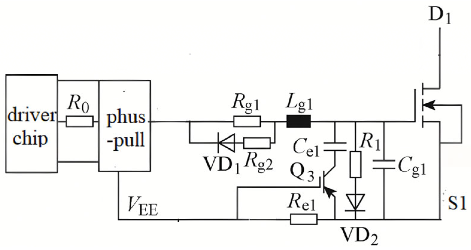
In the drive circuit, improved impedance matching results in reduced current oscillation. The final design of the passive high-disturbance drive circuit, created to eliminate oscillation in the SiC MOSFET drive circuit during high-frequency switching, is illustrated in Figure 4. Each SiC MOSFET’s drive circuit comprises a drive chip and a push–pull amplifier circuit, each with its own independent on-resistance and off-resistance. This configuration allows for the independent control of the gate voltage for each SiC MOSFET, enabling precise on and off turning.
Taking into account factors such as area, power, and heat dissipation, we selected a method that utilizes the impedance characteristics of the magnetic component balance circuit. An iron oxide magnetic bead was connected in series with the on-resistance and off-resistance of each SiC MOSFET. This configuration also helps to suppress the ringing caused by rapid switching in the gate circuit of the SiC MOSFET. The unique high-frequency resistance and low-frequency inductive reactance characteristics of the magnetic beads effectively capture and eliminate high-frequency noise. However, their small inductance values can have a noticeable impact on the leading edge of the pulse. Magnetic beads with high impedance values can effectively suppress the higher harmonics of a pulse; however, they also introduce a relatively large rising edge delay. To minimize the rising edge delay while maintaining effective high-frequency suppression, the size of the magnetic bead can be calculated based on the transient characteristics of the inductance. For instance, the TAIYO YUDEN FB MJ2125 series magnetic beads serve as an example, and the theoretical basis for selecting the impedance of the magnetic bead is provided in Appendix A. The actual impedance values can be adjusted based on experimental results.
Since parasitic oscillation in the gate circuit typically occurs within the frequency range of 50 MHz to 200 MHz, and given that the gate drive switching frequency is 10 kHz with a maximum drive current not exceeding 3 A, the 33 Ω ferrite beads from the TAIYO YUDEN FB MJ2125 series should be selected, as indicated by Formula (A5) in Appendix A. As illustrated in the frequency and impedance relationship curve of the beads shown in Figure 5 (Z represents impedance, R represents resistance, and X represents inductance), the ferrite beads exhibit high impedance within the noise frequency range of 50 MHz to 200 MHz, while demonstrating extremely low impedance at a switching frequency of 10 kHz. The theoretical analysis indicates that the inductance characteristics have a minimal impact on the rising edge. Consequently, it is feasible to maximize the resistance component at the noise frequency to dissipate as much energy as possible, while minimizing the overall impedance at the switching frequency to prevent unnecessary losses and reduce the compromise on the pulse rising edge. It can be stated that the 30 Ω impedance beads in this series are effective in suppressing ringing in the gate circuit of the SiC MOSFET, thereby maintaining relatively stable switching performance. When these beads are used in series with a small driving resistor, gate parasitic oscillations decrease, and simultaneously, switching losses are minimized to the greatest extent.
Additionally, a series circuit consisting of a transistor Q 3 and a capacitor C e 1 is connected to the gate of each MOSFET. When combined with the Kelvin source resistor R e 1 , this configuration can reduce the negative crosstalk voltage generated when each SiC MOSFET tube turns off. As illustrated in Figure 6, when the SiC MOSFET on the bridge arm turns off, the dv/dt of the upper tube rises sharply, while the dv/dt of the lower tube drops sharply, which causes C gd to begin discharging. The discharging current flows in the direction indicated by the solid line arrow in the figure, while the coupling current flows from the Kelvin source terminal S1 to the Kelvin source resistor R e 1 . This enables the transistor Q 3 to turn on, connecting the series capacitor C e 1 to the gate GS and providing a low-impedance path for the coupling current. This effectively suppresses the negative crosstalk and prevents damage to the gate insulation layer of the SiC MOSFET due to excessively high negative voltage caused by the negative crosstalk.

2.3.2. PCB Design of the Drive Circuit

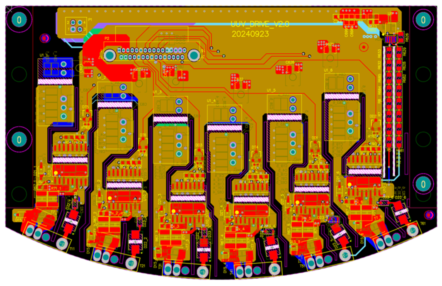
To minimize the coupling and interference between the gate drive loop and the power loop, the gate circuit and the power circuit are placed on separate PCB boards, effectively decoupling the drive circuit from the power circuit. As illustrated in Figure 7, the gate (G) of the SiC MOSFET is soldered onto the drive board along with the Kelvin source (S1). The drain (D) is connected to the power source (S2) via a non-electrically connected through-hole on the drive board, and is then soldered separately to the lower-layer power board. The final design of the driving board PCB is depicted in Figure 8.

2.4. Design of PCB Busbar

2.4.1. Design of PCB Busbar Structure

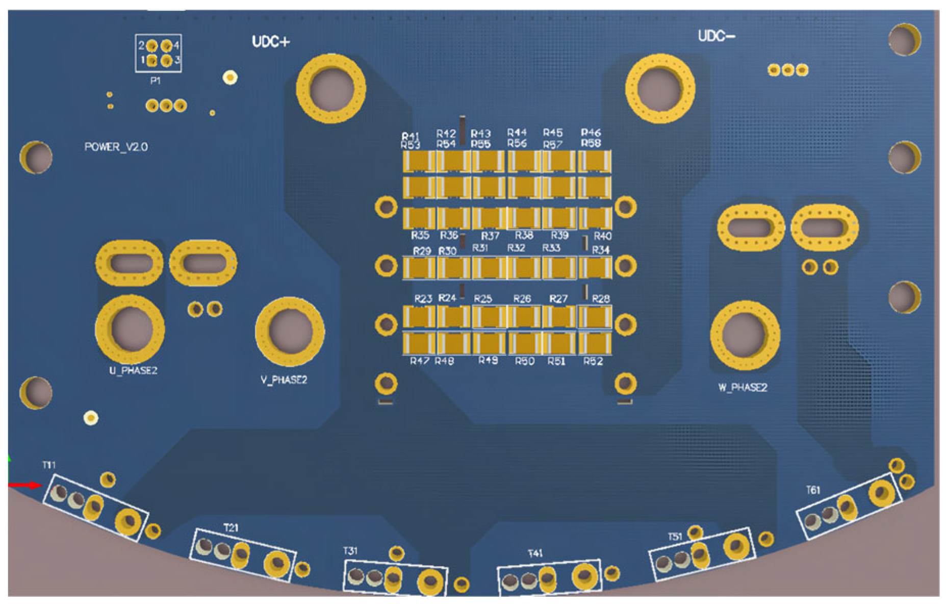
To achieve a high power density for the controller, an integrated design incorporating parallel MOSFET tubes, current sensors, discharge resistors, DC capacitors, and AC/DC terminals was implemented on the PCB bus. Variations in the shapes of the different PCB bus layers, the connection methods of components, and the layout of capacitors all contribute to distinct stacked bus structures. Figure 9 illustrates the schematic diagram of the newly designed PCB bus structure, effectively achieving miniaturization and high power density.
The design aims to create a novel type of PCB laminated busbar structure by minimizing the total self-inductance while maximizing the total mutual inductance. The objective is to achieve optimal power density and effective current equalization characteristics. This is accomplished through a carefully planned layout of the PCB laminated busbar. The PCB busbar comprises multiple groups of vertical multi-loop PCB laminations, with each group consisting of both positive and negative busbars. This configuration enhances mutual inductance and reduces stray inductance. The top and bottom layers of the busbar are equipped with metal windows for both DC and AC routing, as illustrated in Figure 10. Various thicknesses of irregularly shaped metal sheets or strips can be welded together, which not only enhances current flow but also facilitates heat dissipation. The thickness of the external copper sheet must be calculated based on the current carried by the busbar. To ensure a safety margin, the final current-carrying capacity of the busbar is determined to be 1.2 times the actual required current. The thickness of the external copper busbar can be calculated based on the principle that a copper strip with a thickness of 0.035mm and a width of 1 mm can carry 1 A of current, indicating that the current density is 7   A / mm 2 .
The six power-switching devices in the power circuit are evenly arranged around the circular periphery of the busbar, forming a three-phase full-bridge configuration. To optimize space within the controller, two PCB board-level current sensors were utilized. The input of the sensors was connected to the AC terminals of the motor, while the output was linked to the midpoint of the upper and lower parallel pipes. At the three AC connection points, copper columns can be externally welded to establish a direct connection to the motor, ensuring a reliable interface. The DC capacitor is positioned at the center of the PCB busbar and is connected in parallel with the power switching devices of each single-phase bridge. As illustrated in Figure 11, the established model indicates that the capacitor is positioned at the midpoint of the busbar, rather than being located on one side.
With the exception of phase A, the inductance in the two-phase circuits (B phase and C phase) is reduced. In this model, L p , b x ( x = 1 , 2 , 3 ) denotes the inductance between the anode of the upper transistor for phases A, B, and C and the capacitor. Additionally, L n , b x ( x = 1 , 2 , 3 ) represents the inductance between the cathode of the lower transistor for phase A, B, and C and the capacitor. L d , s x ( x = 1 , 2 , 3 , 4 , 5 , 6 ) represents the equivalent inductance at the D pole of each MOSFET; L s , s x ( x = 1 , 2 , 3 , 4 , 5 , 6 ) represents the equivalent inductance at the S pole of each MOSFET; L C A P + and L C A P represents the equivalent inductance at the positive and negative terminals of the capacitor, respectively.
To ensure the stable operation of the circuit, discharge resistors have been installed between the positive and negative terminals of each DC capacitor. This configuration allows the capacitor to maintain its charging and discharging state, even in the event of a power supply change.

2.4.2. Low-Hum Design for Busbars

In the new energy driver, parasitic inductance in the power circuit can generate transient voltage spikes that exceed the withstand voltage range when the power device is turned off. This phenomenon may lead to the breakdown failure of the power device [11]. By analyzing the components contributing to parasitic inductance in the power circuit, we find that the equivalent parasitic inductance of the SiC MOSFET power module and the DC support capacitor is fixed during factory production. Consequently, the only parameter that can be designed and controlled is the inductance of the DC busbar.
A basic laminated busbar structure consists of a conductor layer (positive layer and negative layer) and an intermediate insulating layer. The loop current I flows into the positive layer and out of the negative layer. For a single current loop, energy is stored in the magnetic field in space, and the loop inductance L can be determined based on the stored magnetic energy W n . The formula for this calculation is as follows:
L = 2 W n I 2
For a system composed of multiple parallel current circuits, there is self-induced magnetic energy in each circuit, and there is also mutual magnetic energy between the current circuits. The total magnetic energy W m can be calculated using Formula (5). In the formula, I i represents the current of the i -th loop, I j represents the current of the j -th loop, L i represents the self-inductance of the i -th loop, M i j represents the mutual inductance between the i -th and j -th loops, and N represents the number of current loops If the current circuits are connected in parallel, the equivalent circuit is shown in Figure 12.
W m = 1 2 i = 1 N L i I i 2 + i = j + 1 N j = 1 N M i j I i I j
The total loop inductance L can be expressed as follows:
L = 2 ( 1 2 i = 1 N L i I i 2 + i = j + 1 N j = 1 N M i j I i I j ) ( i = 1 N I i ) 2
From Equation (5), it is evident that decreasing the mutual inductance M i j of the loop can lower the total magnetic energy W m of the loop, which in turn reduces the overall loop inductance L.
If the parallel current circuits display the same impedance and the self-inductance of each circuit is also identical, then the currents in each circuit will be approximately equal. That is,
L 1 L 2 L N I 1 I 2 I N
According to Equation (7), Equation (6) can be simplified as
L = L 1 N + 2 i = j + 1 N j = 1 N M i j N 2
When the currents in adjacent circuits flow in opposite directions, the mutual inductance M i j is negative. L 1 represents the inductance of a single current loop. That is,
L < L 1 N
Therefore, the inductance in a parallel current circuit can be reduced by decreasing the mutual inductance across the entire circuit. When the currents in adjacent circuits of the parallel configuration flow in opposite directions, the overall inductance decreases as the number of circuits increases.
During the commutation process of the device, the frequency of the signals in the circuit is very high, and the current can be considered a high-frequency current. According to reference [27], a basic laminated bus structure consists of conductor layers (positive electrode layer and negative electrode layer) and an intermediate insulating isolation layer. The self-inductance of the double-layer laminated bus is represented as L P and L N , while the mutual inductance is denoted as MN, μ represents the magnetic permeability, l represents the length of the busbar, a represents the width of the busbar, and b represents the thickness of the conductor layer. The formula for calculating the total inductance is
L P ( N ) = μ 2 π l ln 2 l a + b + 1 2 ln ( a + b l ) M N = μ 2 π l ln b 2 + l 2 + l b b 2 + l 2 + b L total = L P + L N ± M N
From the formula, it is evident that the total stray inductance of the laminated busbar depends not only on the inherent characteristics of the conductor layers but also on the mutual inductance between these layers. By reducing the length of the busbar and the distance between the positive and negative poles, one can increase the mutual inductance and decrease the total impedance. Analysis reveals that when the current directions of adjacent layers of the PCB are opposing, a smaller distance between them results in a lower inductance value due to electromagnetic induction between the layers.
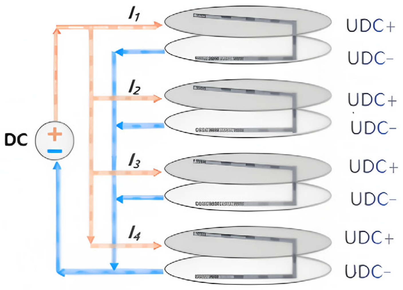
Based on the aforementioned principle, the designed PCB busbar maximizes current-carrying capacity by leveraging the fact that opposing currents in the vertical direction minimize parasitic inductance within the smallest loop area. This design features a single-layer copper thickness of 4 ounces and comprises eight layers, all while maintaining a board thickness of only 2 mm. As illustrated in Figure 13, the board consists of four groups of PCB laminations, with each group containing a positive bus layer and a negative bus layer. Each group forms a loop, where the current flowing through the positive and negative bus layers is equal in magnitude but opposite in direction. The four-loop PCB laminations further reduce the stray inductance of the busbar loop, preventing the power switch device from experiencing significant voltage overshoot during high-speed switching and further minimizing EMI interference. This design ultimately minimizes power loss and improves system efficiency.
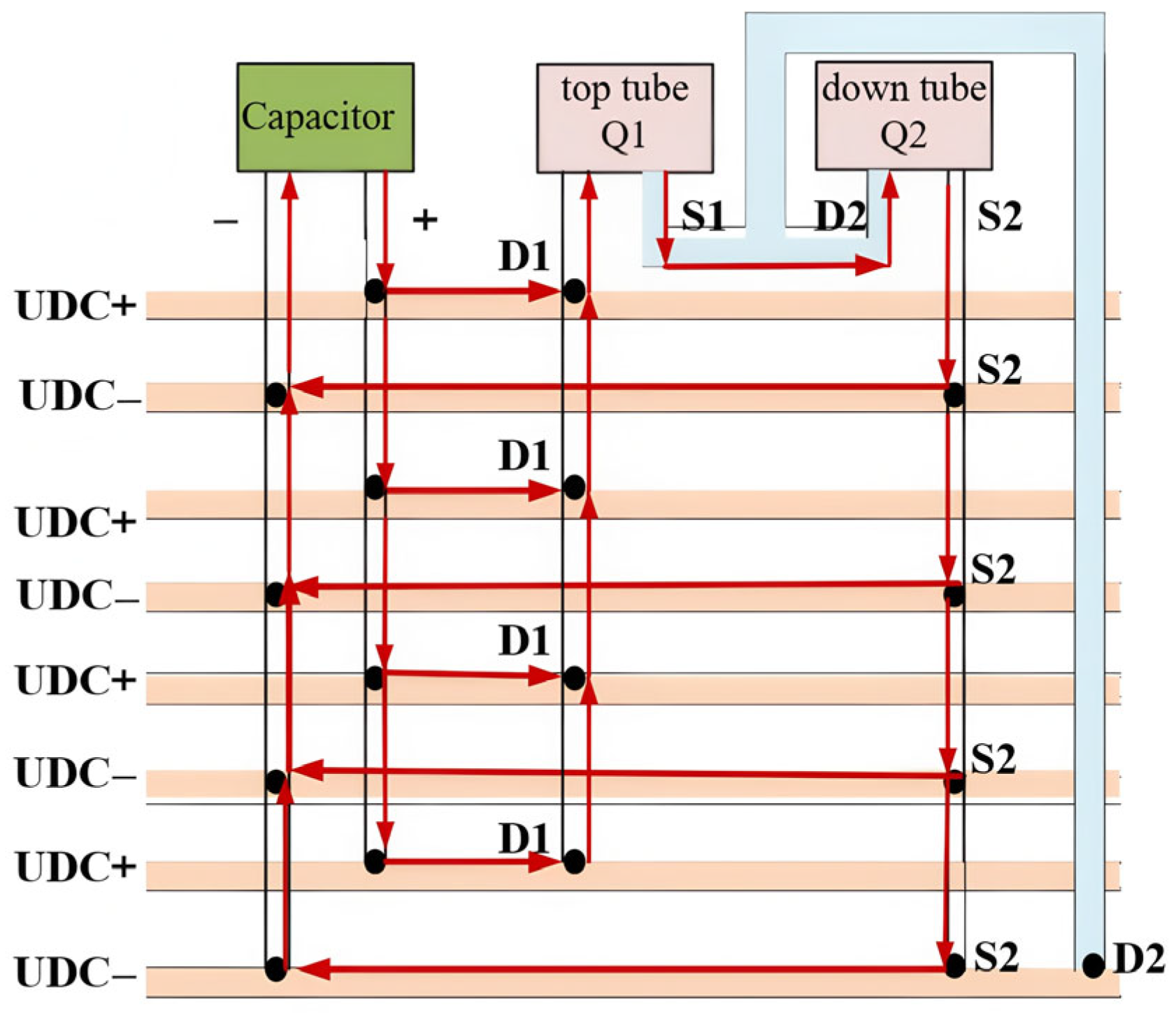
Figure 14 illustrates the current flow direction of the single-loop PCB laminated busbar within the actual printed circuit board (PCB), while Figure 15 depicts the current flow direction of the vertical multi-loop structure PCB laminated busbar. The figures indicate that for each adjacent PCB layer, the current direction is opposing. Additionally, the distance between layers with the same current direction is greater, which enhances the magnetic flux cancellation effect and reduces parasitic inductance. When the parasitic inductance is minimized, it will further decrease the voltage spike during the MOSFET turn-off and reduce electromagnetic interference.

2.4.3. The Inductance Test of Low-Inductance Laminated Busbars

The dual pulses test method was utilized to measure the stray inductance of the busbar. The inductance can be calculated using the slope of the diode current decay d i / d t and the voltage spike V peak at the turn-off voltage.
L loop = t 1 t 2 V peak d t i d ( t 2 ) i d ( t 1 )
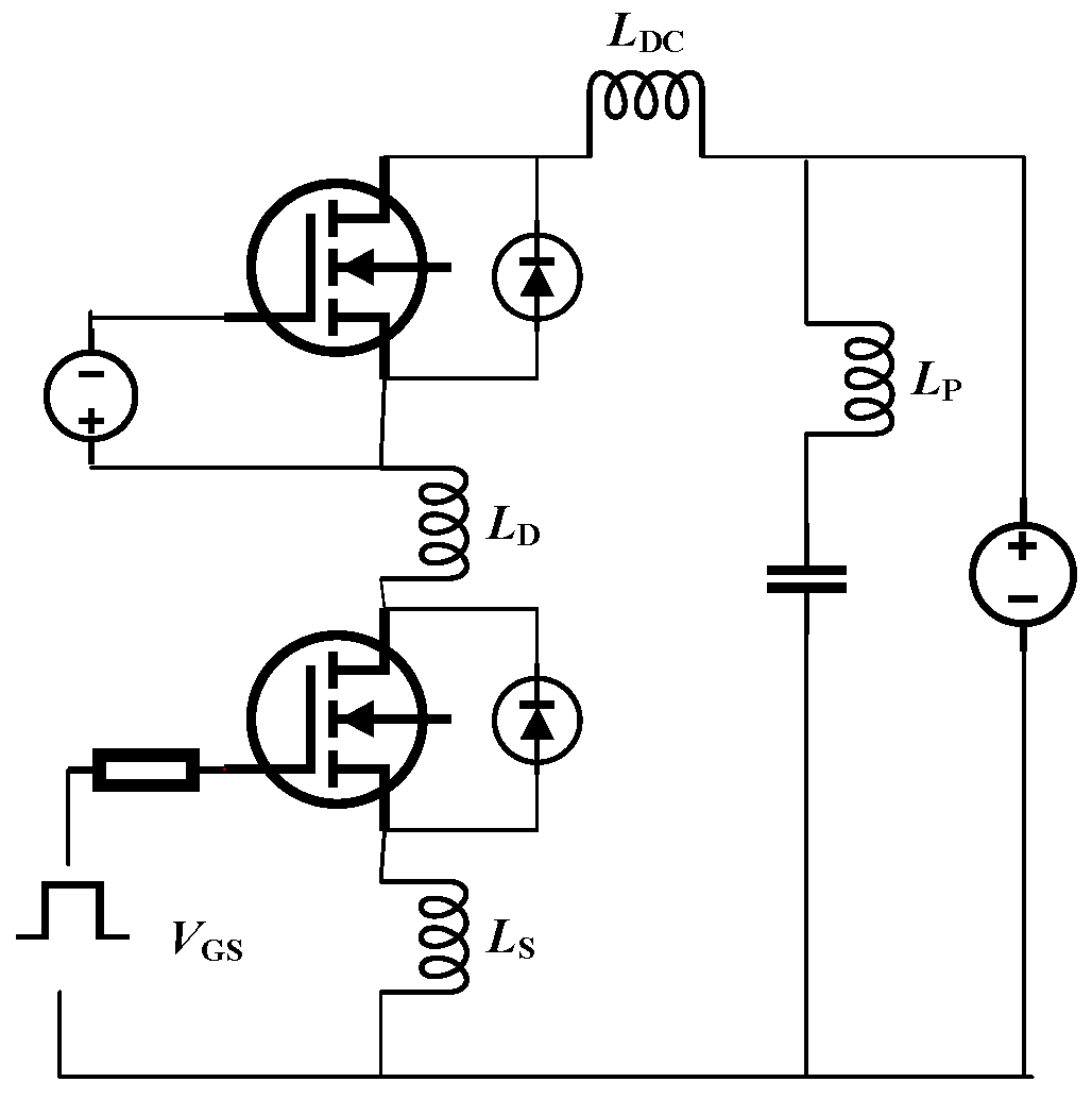
The composition of the dual-pulse power loop inductors is illustrated in Figure 16. It primarily consists of the parasitic inductor L P associated with the bus capacitor, the DC busbar inductor L DC , and the source inductor L S and drain inductor L D on the MOSFET.
L loop = L d + L DC + L P L d = L S + L D
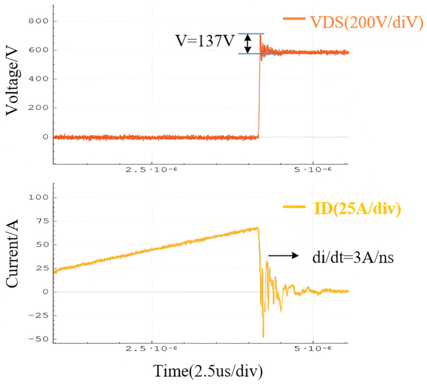
During the testing process, in order to reduce the influence of parasitic capacitance and inductance on the measurement results, we used an optical isolation probe to measure the voltage across the SiC MOSFET and used a Rogowski coil to measure the drain current. Figure 17 shows the voltage and current waveforms under the 600 V/68 A dual-pulse test. Using this process, the busbar inductance was calculated.
After conducting research, it was determined that measurement errors of voltage and current, as well as inaccuracies in selecting the time period for the rate of current change, may result in a deviation between the measured inductance value and the actual value. Table 1 presents the extracted stray inductance values for each component in the power circuit under the conditions of 600 V and 68 A. When calculating the inductance of the laminated busbar, the power circuit inductance is derived from the measurement obtained during the double-pulse experiment. The double-pulse waveform indicates that the overshoot of the turn-off voltage is 137 V, with a current change rate of 3 A/ns. Consequently, the loop inductance L loop is approximately 45 nH. The parasitic inductance L d of the SiC MOSFET is measured using an impedance analyzer, while the parasitic inductance L P of the busbar capacitor is obtained from the data sheet. To prevent frequency-dependent errors resulting from parasitic capacitance and inductance during inductance measurements, an impedance analyzer equipped with a parameter compensation function was utilized. Ultimately, the stray inductance value on the PCB busbar L DC is determined to be 15 nH.
To verify the accuracy of the experimental measurements of the stray inductance in the printed circuit board bus lines and to assess whether the results of the proposed method align with previously calculated values when compared to findings from traditional methods, Ansys Q3D 18.2 software was utilized to simulate both the vertical multi-loop busbar structure and the single-loop busbar structure. The simulation diagram of the busbar in Q3D is shown in the Figure 18; the simulation frequency was set to 30 Hz. The resulting parasitic inductance values for the bus structures are presented in Table 2. A comparison of the data reveals that, although the simulated inductance values for the vertical multi-loop busbar structure differ from the experimental values, they remain within an acceptable error range. Furthermore, the inductance value of the vertical multi-loop busbar structure is reduced by more than 42% compared to that of the single-loop busbar structure. The simulation values are not as ideal as the theoretical calculated values. This misalignment is due to several factors, including the incomplete alignment of the positive and negative terminals of the busbar, as well as the layout of the capacitors.
Table 3 presents a comparison between the bus inductance achieved by this research method and that obtained from existing references. The inductance value achieved through this research is comparable to results reported in other studies. This similarity arises from the fact that there is no one-size-fits-all solution for busbar design; it is highly dependent on the specific application and the mechanical integration with the power modules. Furthermore, the design of the busbars is closely related to power density. This study successfully developed a busbar design for both AC and DC power supplies on a PCB board, achieving high power density, albeit at the expense of the capacitor layout structure.

2.5. Thermal Design

2.5.1. Loss Calculation

The power loss generated by SiC MOSFET power devices during operation constitutes the majority of the total power loss in the inverter. Therefore, to effectively minimize this loss, it is essential to implement efficient heat dissipation techniques. Additionally, precise numerical calculations should be conducted to determine the optimal heat dissipation strategy, which will help reduce losses and ensure the normal operation of the control system. The power loss of SiC power devices in the motor controller’s power circuit primarily consists of switching loss and static loss. The switching loss is further categorized into on-state loss and off-state loss, while the static loss is divided into conduction loss and cutoff loss.
The SiC MOSFET discrete devices with TO247 packaging are utilized as power devices in the controller. When the MOSFET is in the forward conduction state, the diode connected in parallel remains in the off state, similar to the IGBT module. Notably, when the diode conducts, the MOSFET also conducts in reverse. However, due to the MOSFET’s conduction resistance R CE being significantly lower than that of the diode, the total current I p flowing through the two devices in parallel predominantly passes through the MOSFET, resulting in a minimal current flowing through the diode. The reverse conduction loss of the MOSFET is included in the calculations. The forward conduction loss P cond _ T and reverse conduction loss P cond _ D of the MOSFET can be calculated using Formulas (13) and (14). In the formula, V CE 0 is the intercept of the forward conduction voltage–current curve of the MOSFET; V F 0 is the intercept of the reverse conduction voltage–current curve of the MOSFET; R F is the reverse conduction resistance of the MOSFET.
P cond _ T = 1 2 π + m cos φ 8 V CE 0 I p + 1 8 + m cos φ 3 π m 75 π R CE I p 2
P cond _ D = 1 2 π m cos φ 8 V F 0 I p + 1 8 m cos φ 3 π + m 75 π R F I p 2
The switching losses P swit _ T of a MOSFET can be calculated using Formula (15), and the switching losses P rec _ D of a MOSFET parallel diode can be calculated using Formula (16). In the formula, f s represents the switching frequency; E on is the on-state loss of the MOSFET under rated current and rated voltage; E off is the off-state loss of the MOSFET under rated current and rated voltage; E rec is the off-state loss of the diode; V dc is the DC bus input voltage of the module; V nom and I nom are the voltage and current measured when calculating the switching loss.
P swit _ T = 1 π f s E on + E off V dc I p V nom I nom
P rec _ D = 1 π f s E rec V dc V nom 0.45 I p I nom + 0.55

2.5.2. The Structural Design of Heat Dissipation

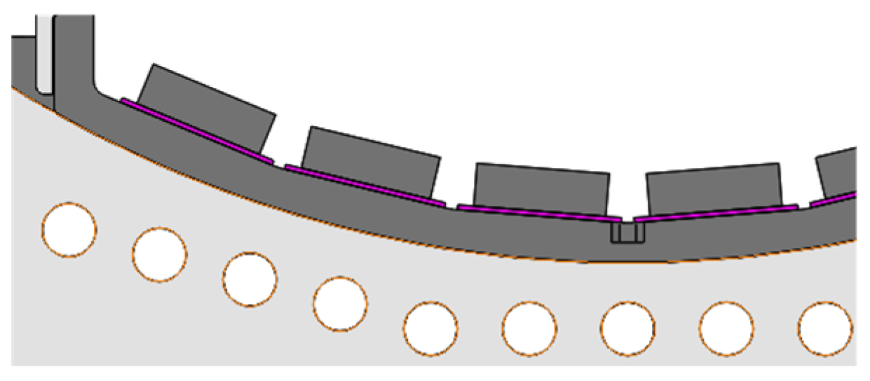
Since the motor controller is mounted on the casing and cooled by external water, the primary heat-generating components, SiC MOSFETs, are evenly distributed along the cylindrical shell section of the casing during the design phase. Heat is directly transferred to the outer surface through thermal conduction. The drive and control circuits generate minimal heat and utilize high-temperature components rated for 125 °C. They are cooled by the natural convection of air within the casing and do not require additional cooling, and there is no effect the module’s overall cooling efficiency. A total of six TO247-4 packaged SiC MOSFET modules are employed in the control system. The installation surface width of each module is approximately 16 mm. Considering a necessary installation gap, the maximum side length of the area where each device must be installed and cooled is about 23 mm. Therefore, the circumference of the required heat sink should be no less than 138 mm, as illustrated in Figure 19.
Because the surface of the SiC MOSFET module installed on the casing serves as the live drain, insulation treatment must be considered during the installation process to ensure both effective heat dissipation and optimal electrical performance. In this context, electrical isolation is achieved by placing an insulating ceramic sheet between the module and the casing. It is essential that the dimensions of the ceramic sheet exceed those of the module’s installation surface. The common ground for the six SiC MOSFETs is located on the power board. The source pins (S) of the three lower-power transistors in the three bridge arms are soldered to the power board and connected to the negative busbar. Similarly, the drain pins (D) of the three upper transistors are also soldered to the power board and connected to the positive busbar.
Assuming that the module loss is uniformly distributed, the heat dissipation path for the module loss is as follows: module → ceramic gasket → controller housing → chassis → water, as illustrated in Figure 20.
The cooling structure of the controller is illustrated in Figure 20. Based on the thermal properties and dimensions of each material layer, the thermal resistances of each component were estimated. The effective heat dissipation area of the shell is approximately equal to the area of the ceramic sheet, which in turn is approximately equal to the base area of the module. The convective heat transfer thermal resistances listed in the table are calculated using an empirical formula and are taken to be 5000 W/m2K. The distribution of heat resistance for the power module’s heat dissipation is presented in Table 4.
According to the loss calculation Formulas (13)–(16), when the controller operates at a peak power of 10 kW, with a bus voltage of 600 V and a switching frequency of 50 kHz, the total loss of the controller is 330 W, and the loss (P) per module is 55 W. Calculated based on the loss data at the peak steady state condition, when the water temperature T f is ≤40 °C, the junction temperature T j max , calculated using Equation (17), is 124 °C, which does not exceed the maximum allowable temperature of 175 °C. This ensures compliance with the device’s safety operation requirements and provides a significant margin for safe operation.
T j max = R j f P + T f

2.6. Software Algorithm Design

To evaluate the controller’s performance, a test rig for the platform frame was assembled. The dynamometer served as the load motor and operated in torque mode, dynamically adjusting the load torque. The controller and its associated motor functioned as drive motors, operating in speed mode. The control algorithm employs a dual closed-loop structure, comprising an outer speed loop and an inner current loop, along with traditional Space Vector Pulse Width Modulation (SVPWM) and Proportional–Integral–Derivative (PID) control algorithms. The block diagram of this structure is shown in the Figure 21. With this structure, the system accounts for both dynamic response and robustness, making it a classic solution for motor control. The motor system is frequently affected by factors such as sudden load changes, parameter drift (for example, the impact of temperature on resistance), and nonlinear friction. Traditional PID controllers depend on precise mathematical models and struggle to adapt to these conditions. References [28] and [29], respectively, proposed a new type of fuzzy logic algorithm and algorithms based on Q-learning (QL) and deep Q-network learning (DQNL). We will build upon these algorithms in subsequent work by combining fuzzy logic with adaptive algorithms, as well as Q-learning (QL) and deep Q-network learning (DQNL) with adaptive algorithms, to enhance high-performance motor control.
The controller’s software protection functions include overcurrent protection, overvoltage protection, overtemperature protection, and overspeed protection. These protection thresholds can be customized according to specific requirements. When any threshold is exceeded, the system will shut down. The software protection detection cycle operates in sync with the power device switching cycle.

2.7. Design of Control Circuit

2.7.1. Design of Fault Protection

The AC current sampling in the controller is performed using the LEM’s current sensor to provide isolation from the motor. The voltage sampling is performed using an isolated differential amplifier circuit that incorporates the AMC1311DWVR isolation chip and an isolated power supply, which ensures isolation between high- and low-voltage systems and improves noise immunity. The hardware protection of the controller is primarily implemented through a CPLD, which includes three-phase AC current overcurrent protection, DC voltage overvoltage protection, and three-phase IGBT fault protection. All fault signals are processed by the CPLD and then sent to the interrupt pins of the DSP. The DSP evaluates these signals and issues a software blocking command accordingly. Additionally, the overcurrent signals from the three-phase AC currents are processed by the CPLD and output as overcurrent signals to the DSP’s IO pins, enabling the system to distinguish whether the interrupt fault signals correspond to overcurrent conditions. The principal block diagram of the fault protection circuit is shown in Figure 22.
Protection strategies are divided into two levels: the first level is software protection, and the second level is hardware protection. The protection logic program within the software is situated between the user layer program and the current loop program. It evaluates various operating status parameters from the signal acquisition module to determine if a fault is occurring. Depending on the fault’s cause, it implements different response measures, including appropriately limiting the current command output generated by the user layer program.

2.7.2. Design of CAN Communication Circuit

Figure 23 shows the schematic diagram of the CAN bus interface circuit. The DSP chip includes a CAN controller module that supports the CAN 2.0B protocol. Therefore, only one CAN transceiver is required in the CAN interface circuit. The CAN transceiver model is TJA1042T, which converts the DSP’s TTL level signals to the differential level (2 V) used on the CAN bus. The TJA1042T is specifically designed for automotive CAN communication and supports a maximum transmission speed of up to 1 Mb/s. To enhance the anti-interference performance of the CAN interface, an electromagnetic isolation device, the ADuM1201, is placed at the front end of the CAN transceiver to provide photoelectric isolation of the TTL signals. Additionally, filter capacitors CH, CL, and CDF are used to suppress noise interference on the CAN bus, and the CAN bus transient voltage suppressor NUP2105L is employed to protect against surge voltages on the bus. These components collectively improve the anti-interference capability and reliability of the CAN interface.

2.8. Design of Electrical Parameters for Filtering Components

The filtering circuit of the low-voltage power supply effectively suppresses multi-dimensional noise, significantly reducing electromagnetic interference (EMI) to the power grid and minimizing external radiation, while enhancing the system’s anti-interference capability. The principal block diagram of the 28 V input filtering circuit is shown in Figure 24, and parameter optimization was performed through simulation.
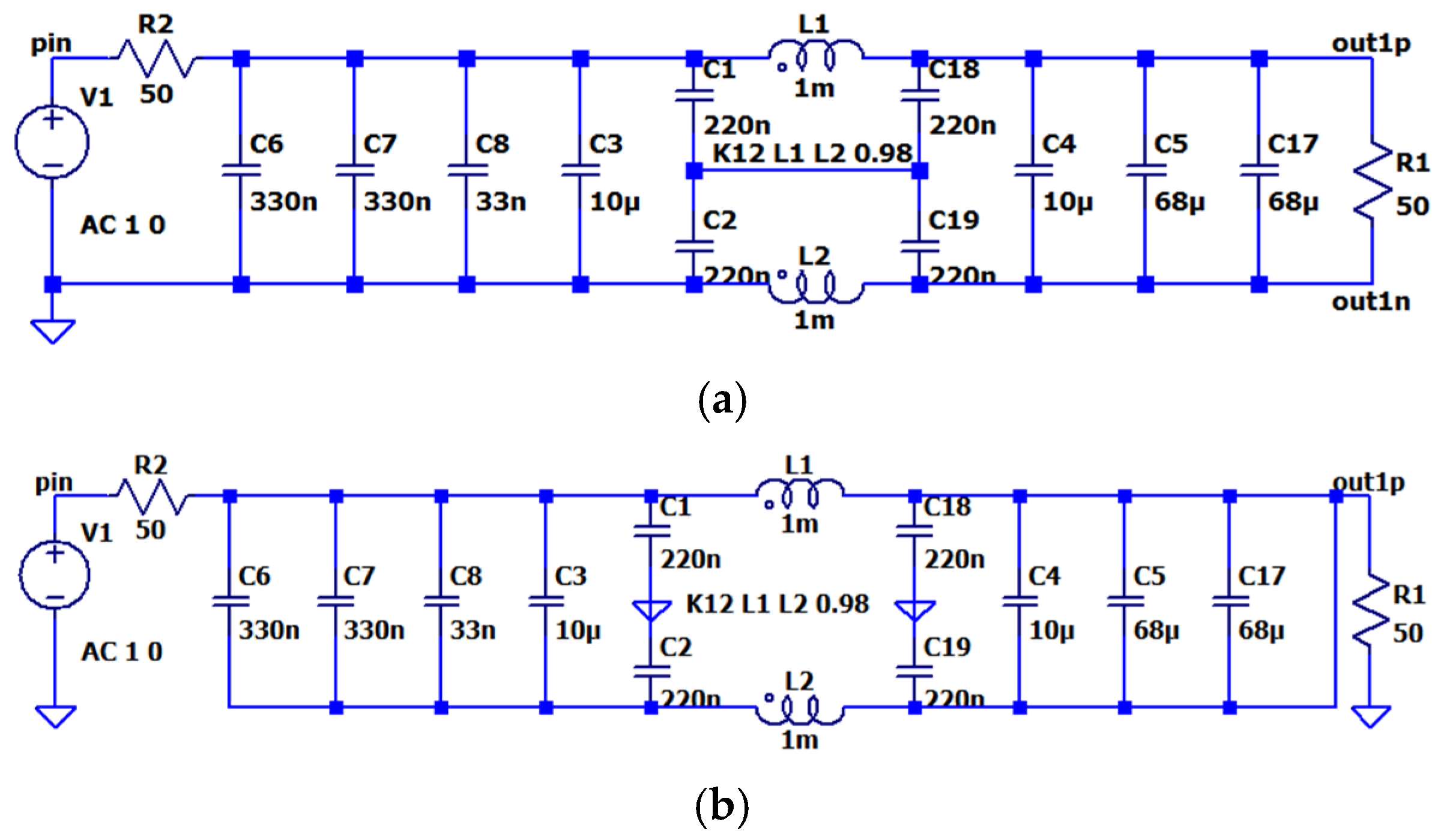
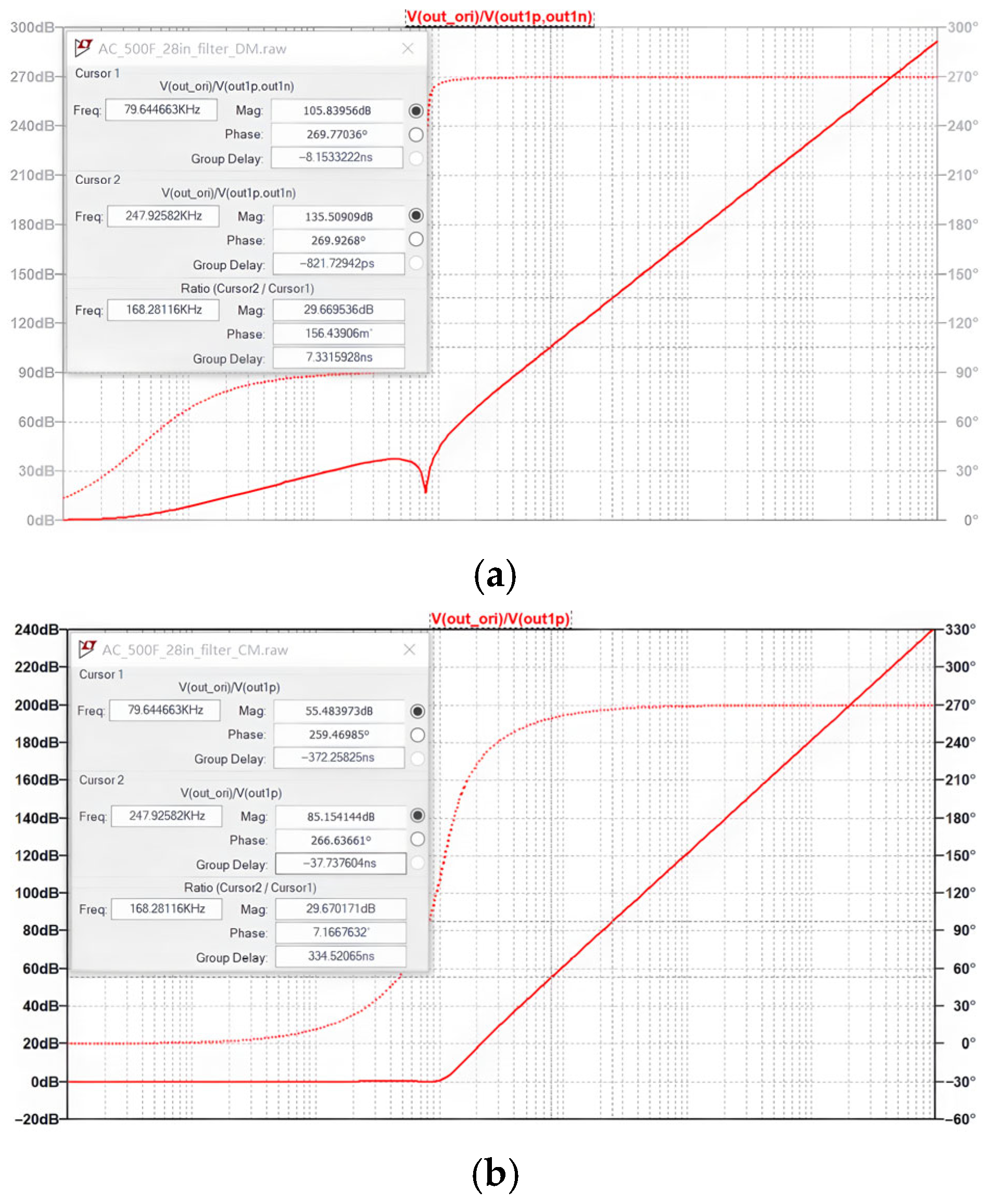
The simulation evaluated the insertion loss of each EMI filter circuit. In the simulation, both the input and output port resistances were set to 50 Ω, and all filter components were modeled as ideal devices. The simulation circuit is shown in Figure 25, and the results are presented in Figure 26. The switching frequency of the power module is approximately 250 kHz. At this frequency, the designed EMI filter circuit provides approximately 135 dB of differential mode insertion loss and approximately 85 dB of common mode insertion loss. Above the switching frequency, the differential mode insertion loss increases at a rate of 60 dB/decade, and the common mode insertion loss also increases at 60 dB/decade.

3. The Prototype and Test of a High-Switching-Frequency Controller for SiC MOSFET Discrete Devices

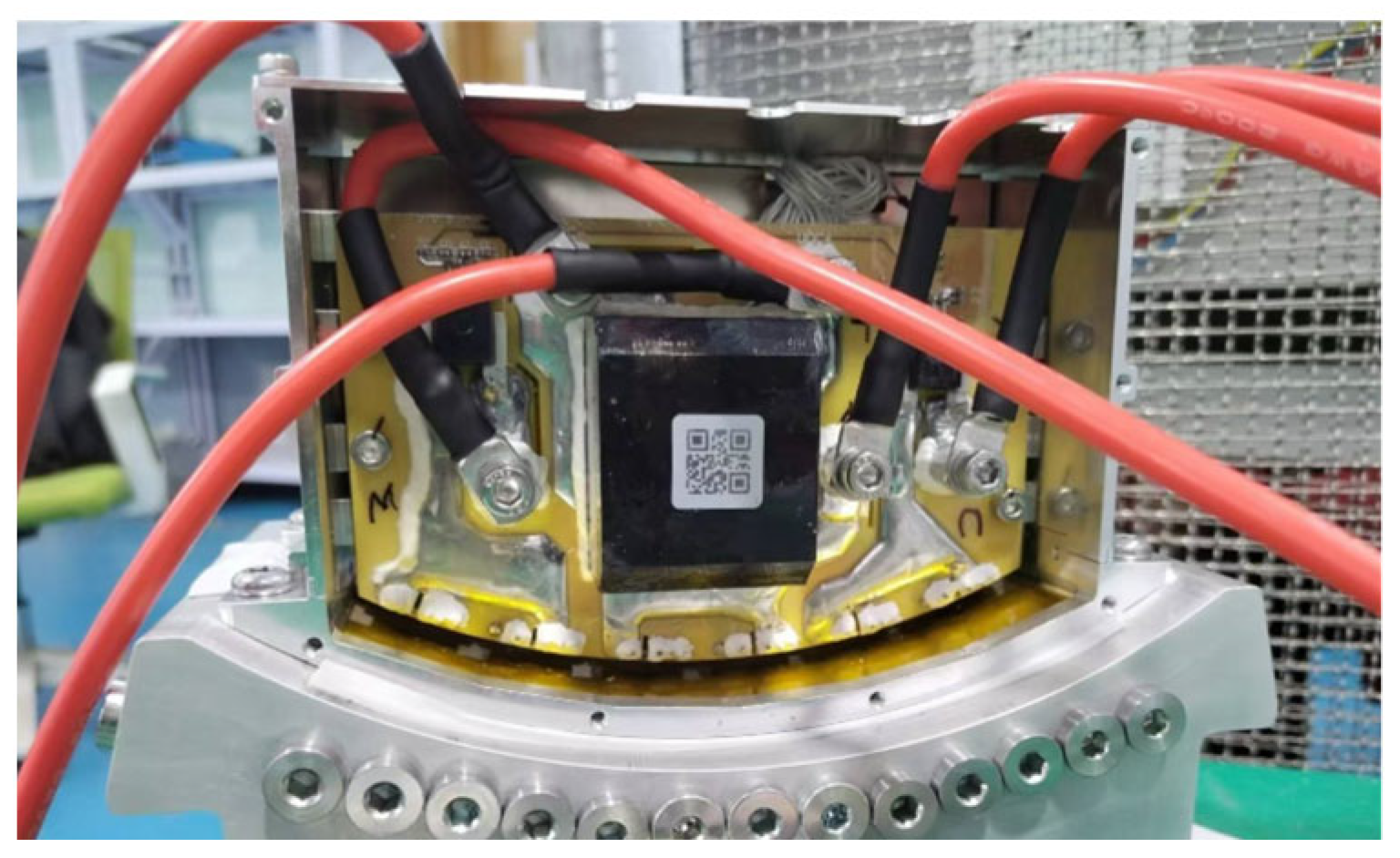
By adopting the key component design method for SiC MOSFET discrete devices, a prototype for a high-switching-frequency SiC controller was designed and fabricated. This controller operates at an input voltage of 600 V, with a peak output power of 10 kW. It weighs 1.116 kg, resulting in an impressive power-to-weight ratio of 9 kW/kg. The appearance of the controller is illustrated in Figure 27. The power density is notably high, and the compact circuit design not only optimizes system space but also helps reduce the parasitic inductance of the drive circuit.

3.1. Dual-Pulse Test

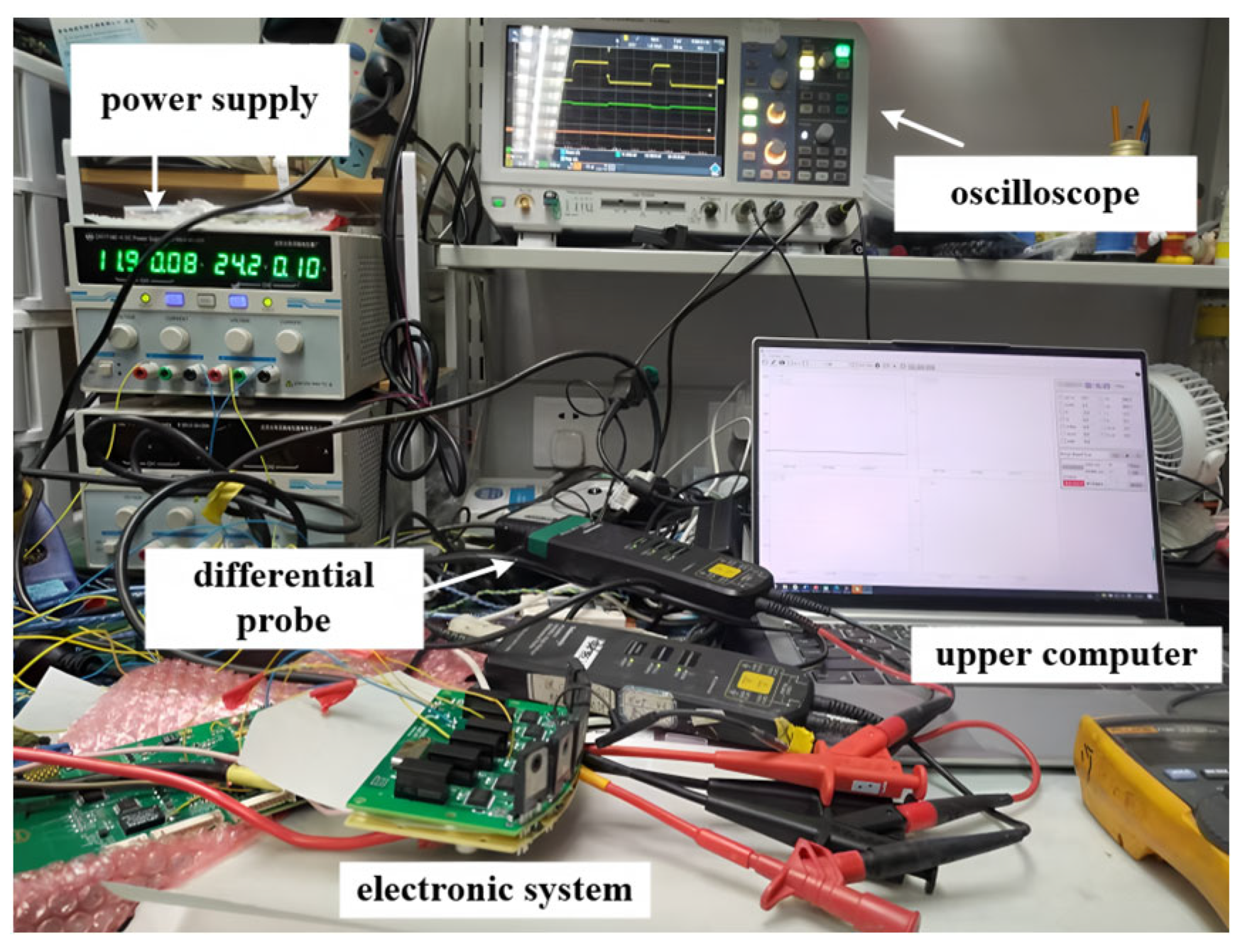
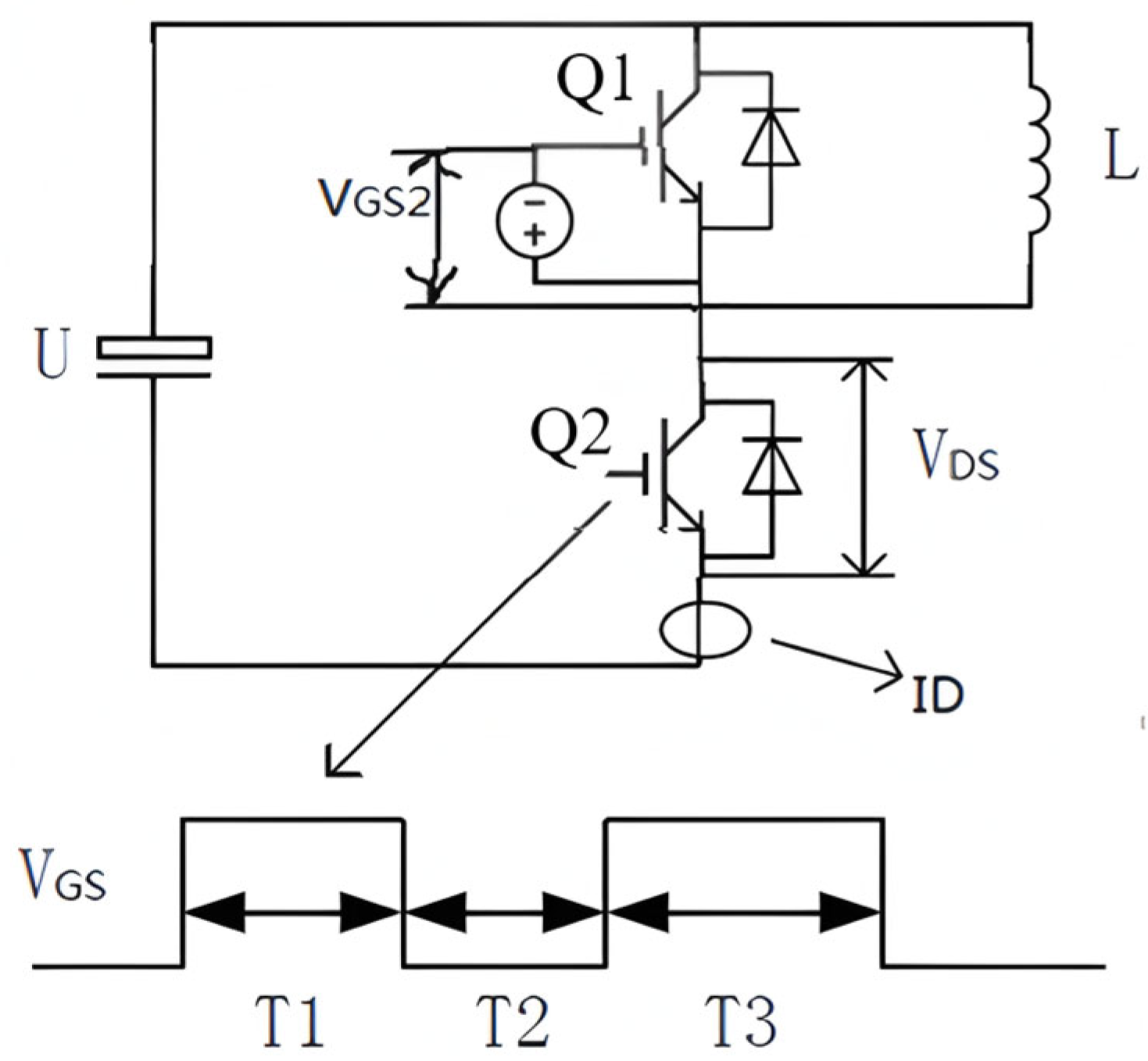
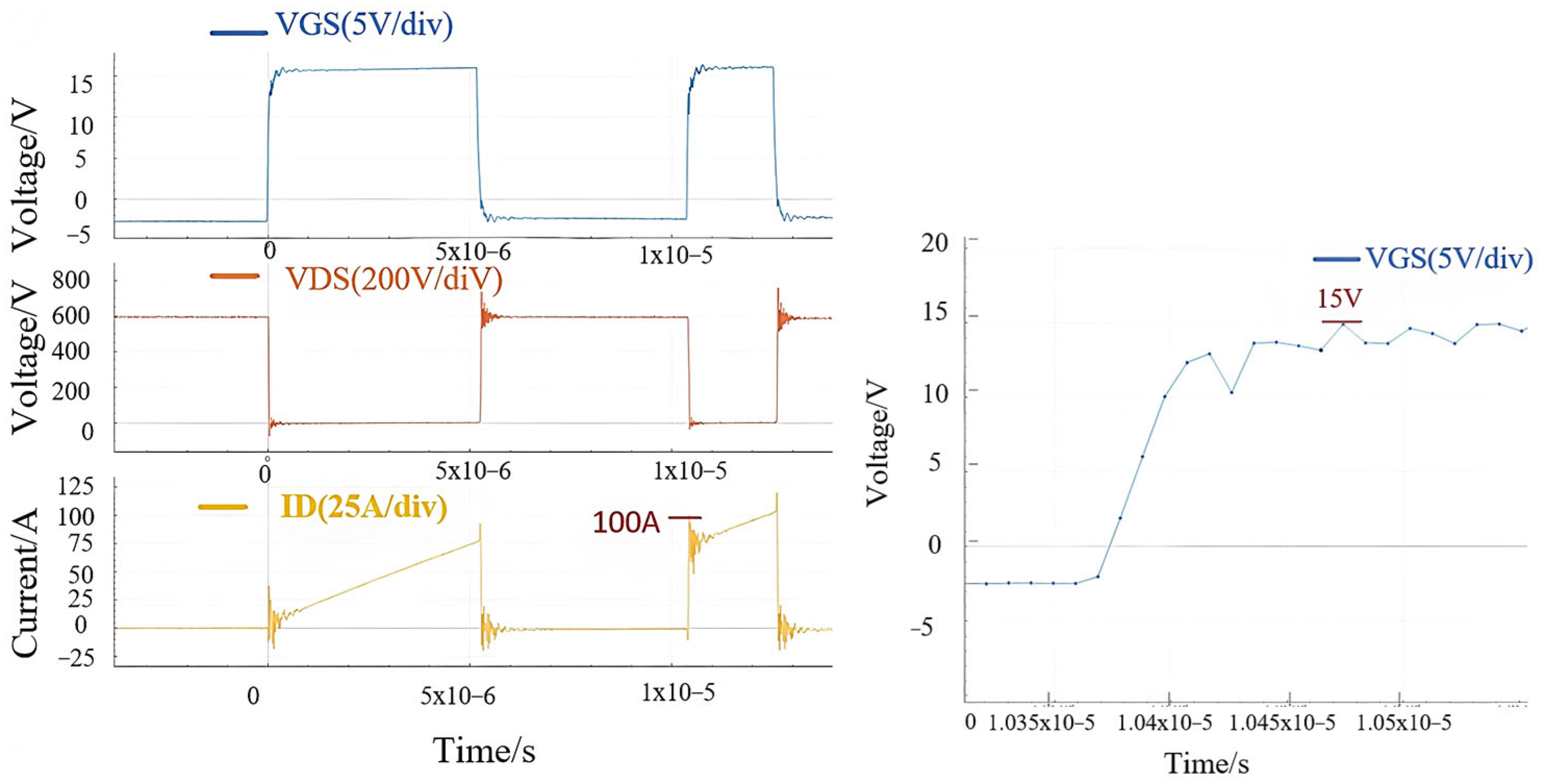
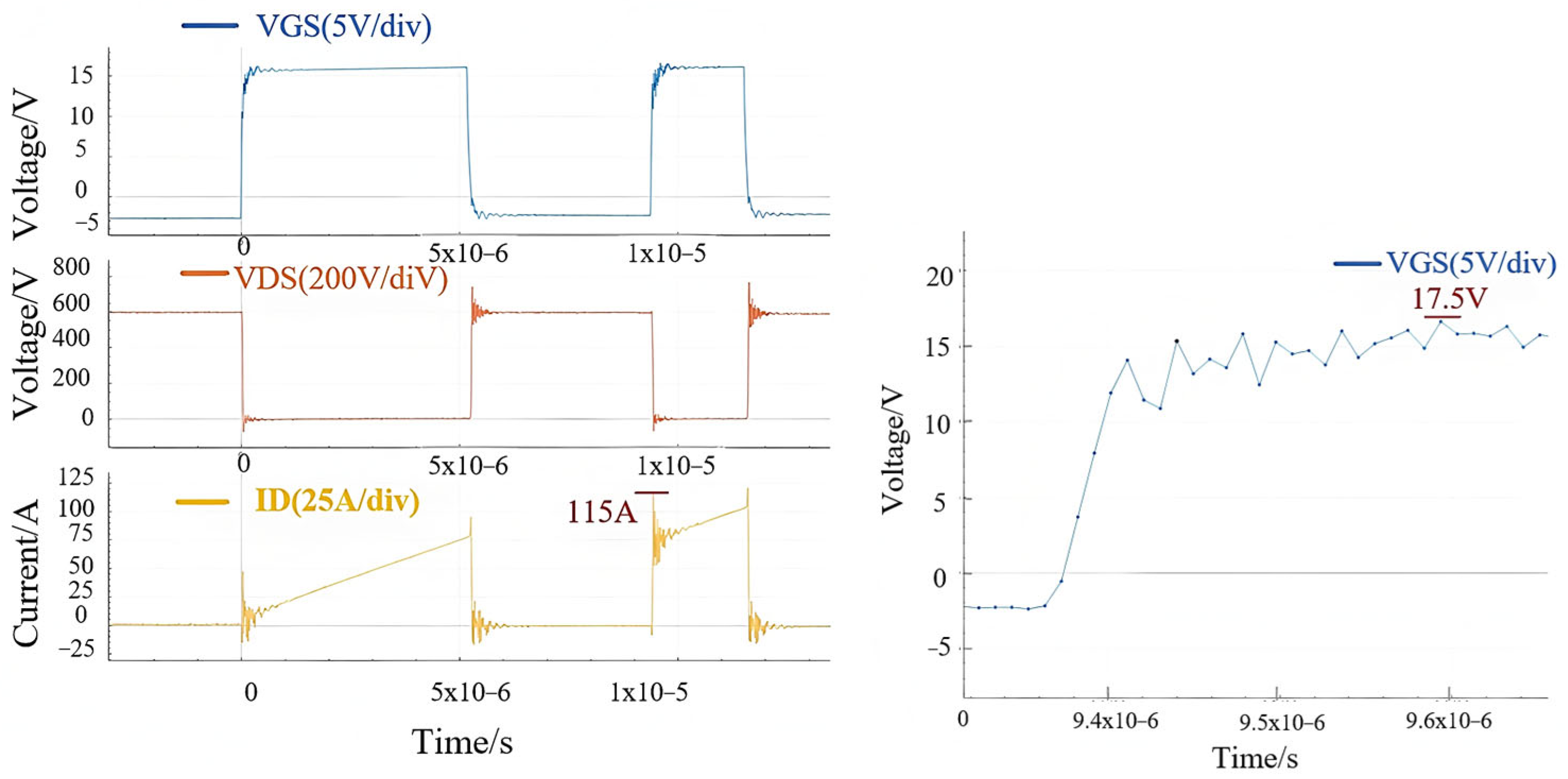
To verify the switching performance of the system at a bus voltage of 600 V, a dual-pulse test was conducted on the electronic system. The test conditions included a bus voltage of 600 V, a maximum load current of 68 A, a driving resistance of 3 Ω, and a load inductance of 45 µH. A photo of the dual-pulse experiment is shown in Figure 28. The voltage measurement utilized two differential probes, model TT-SI 8071, with a bandwidth of 200 MHz, while the current measurement employed a Rogowski coil with a bandwidth of 50 MHz. The wiring and test point positions for the dual-pulse test are illustrated in Figure 29. To measure the drain current of the lower transistor Q2 in the test bridge arm, the Rohs coil should be connected to the source terminal of Q2. To measure the drain-source voltage (VDS), the differential probe should be connected between the drain and source terminals of Q2. To measure the gate voltage (VGS), the differential probe should be connected between the gate and source terminals of Q2. The dual-pulse test waveform is illustrated in Figure 30. Figure 31 illustrates the dual-pulse test waveform using the conventional drive circuit. Upon comparison, it is observed that, in contrast to the results of the conventional method, the maximum gate voltage oscillation in the proposed drive method has decreased from 17.5 V to 15 V, representing a reduction of 11%. Additionally, the maximum drain current has decreased from 115 A to 100 A, which is a reduction of 13%. Furthermore, the switching loss has decreased from 570 mW to 480 mW, indicating a reduction of 15.7%. The measurement error resulting from parasitic capacitance and inductance has not been considered in this analysis. The light blue line represents the driving VGS voltage signal, the red line indicates the VDS voltage of the MOSFET under test, and the dark blue and black lines represent the ID current measured by the Rogowski coil for the two parallel transistors. From the test waveforms, it is evident that this parallel system can reliably turn on and off under the operating conditions of 600 V/68 A, thereby meeting the maximum operational requirements of the controller.

3.2. Power Experiment

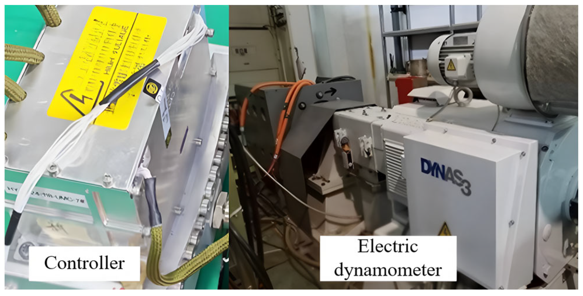
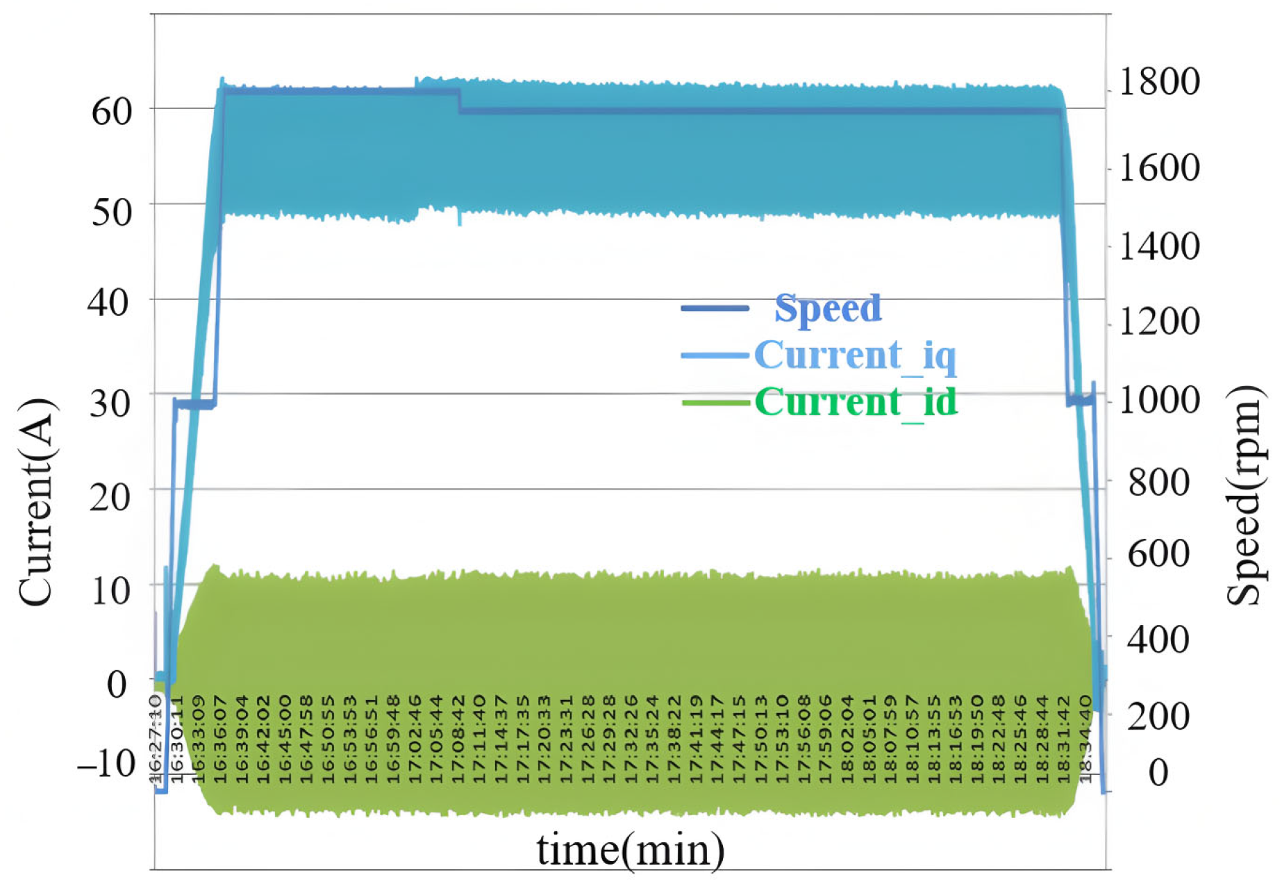
During the power test, the dynamometer served as the load motor and operated in torque mode, dynamically adjusting the load torque. The controller and its associated motor functioned as drive motors, operating in speed mode. The system’s efficiency and various electrical parameters are measured using a power analyzer. The data upload rate from the upper computer was 200 milliseconds per data point, and the test duration was 5 min. The DC power supply consists of an 850 V power cabinet, which features constant voltage and current limiting capabilities. Both the controller and the motor are mounted on the test bench, and cooling water is circulated through the controller’s heat dissipation fixture, maintaining a flow rate of no less than 3 L/min. The maximum DC bus voltage is 600 V, and the maximum rotational speed of the motor reaches up to 1800 r/min. Figure 32 illustrates the power experimental platform of the SiC MOSFET controller. Figure 33 and Figure 34 display the experimental data recorded by the host computer over a duration of 5 min. The data upload speed is 200 milliseconds per instance. As illustrated in the figures, the controller operates reliably for extended periods across various rotational speeds and currents, without experiencing any faults or electromagnetic interference. During the gradual loading of the dynamometer, the control system can maintain a constant rotational speed. In addition, a 10 kW peak power test was conducted on the 600 V bus voltage. In order to evaluate the current-carrying capacity and heat dissipation performance of the designed PCB laminated busbar, an infrared thermal imager was utilized to monitor the temperature of the busbar. Figure 35 shows the temperature distribution map of the PCB bus board. This image was captured when the controller reached its peak power of 10 kW. As illustrated in the figure, the maximum temperature on this printed circuit board is 54.7 °C, indicating an increase of 22 °C from the initial ambient temperature. The heat dissipation performance is exceptionally effective.
Figure 36 presents the waveform of the long-term test data over a period of 7 h at room temperature of 29 °C, with relative humidity ranging from 40% to 60%. These data were stored by the host computer and recorded by the power analyzer, including the actual waveforms of the motor phase currents, the torque, the rotational speed, and the temperature of the controller housing. The output storage time was 200 ms per point. The maximum current and rotational speed during long-term operation are 36 A and 1000 rpm, respectively, and the maximum torque output of the dynamometer is 900 Nm. When the running time of each condition exceeded 5 min, the inner wall temperature of the controller housing basically reached the thermal equilibrium state. The final inner wall temperature was 41 °C. At this point, according to Table 3 and Formula (17), the junction temperature of the MOSFET was approximately estimated using the total thermal resistance (excluding the convective heat transfer thermal resistance and the thermal resistance of the water channel housing) as 82 °C, which met the usage requirements. The temperature of the housing was measured using a PT1000 sensor near the MOSFET module on the inner wall of the controller housing, and the temperature values were directly read by the host computer. To prevent the controller from overheating, the host computer continuously monitors the controller’s temperature in real time. The temperature sensor, after being processed by the conditioning circuit, is sampled by an analog-to-digital converter (ADC) and then uploaded to the digital signal processor (DSP). If the detected temperature exceeds the protection threshold established by the DSP, it will either reduce power operation or shut down the system.
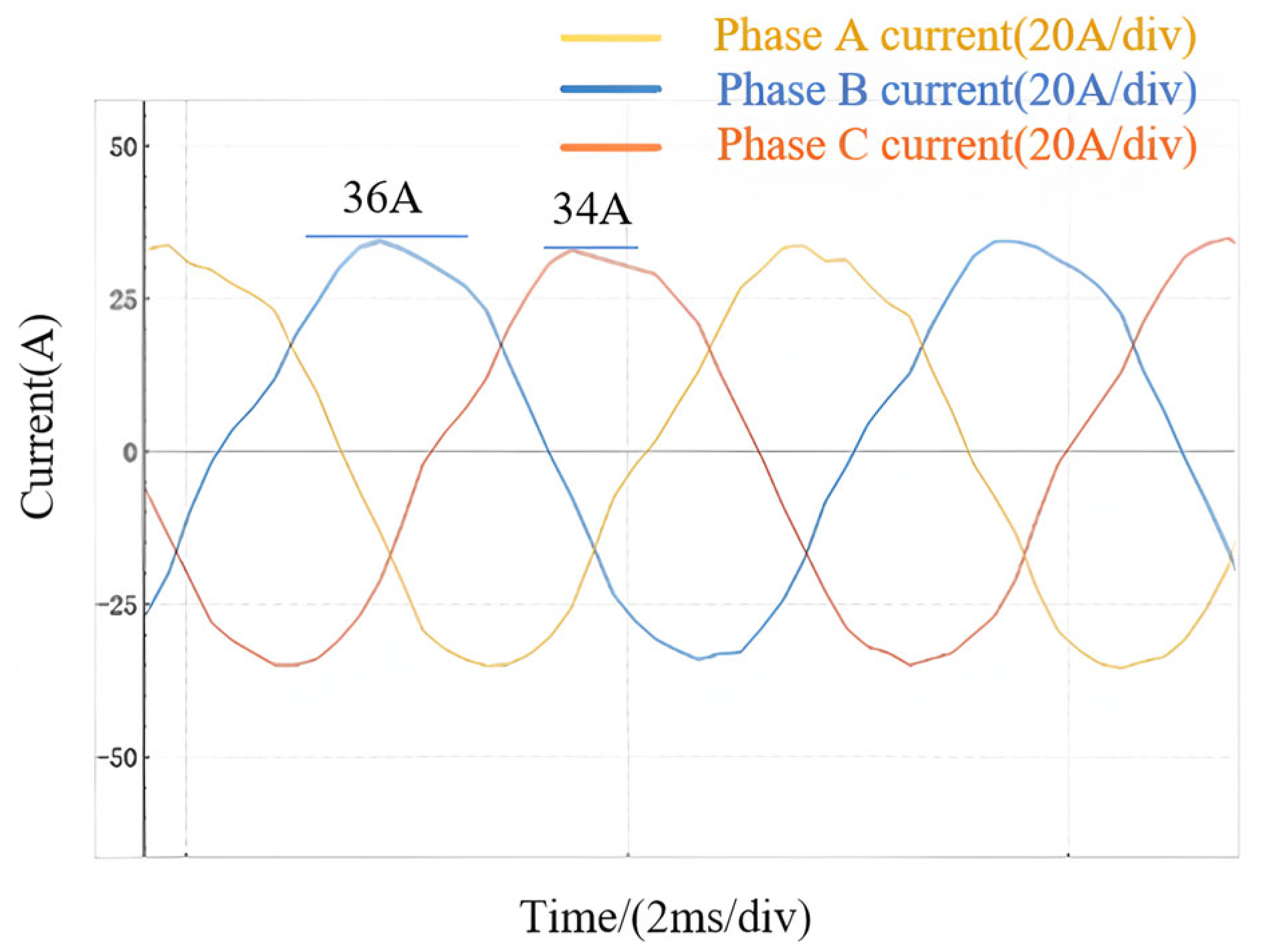
Figure 37 shows the steady-state current waveform when the peak current reaches 36 A. The waveform indicates that the RMS values of the AC currents for phase A and phase B are both 36 A, while the RMS value for phase C is 34 A. The degree of imbalance in the three-phase AC current is 2.8%, which is relatively acceptable, indicating that the controller is functioning well.
To evaluate the motor’s power generation performance, the dynamometer on the test bench was used as the prime mover to provide rotational speed. After developing the controller, it was connected to the load box to conduct the power generation test. Figure 38 shows the test waveforms of the power generation command and the load voltage as the power was gradually increased to the full capacity of 10 kW and then decreased back to 0 kW during the experiment. It can be observed that during both the loading and unloading processes, the power generation voltage quickly tracked the power generation command.
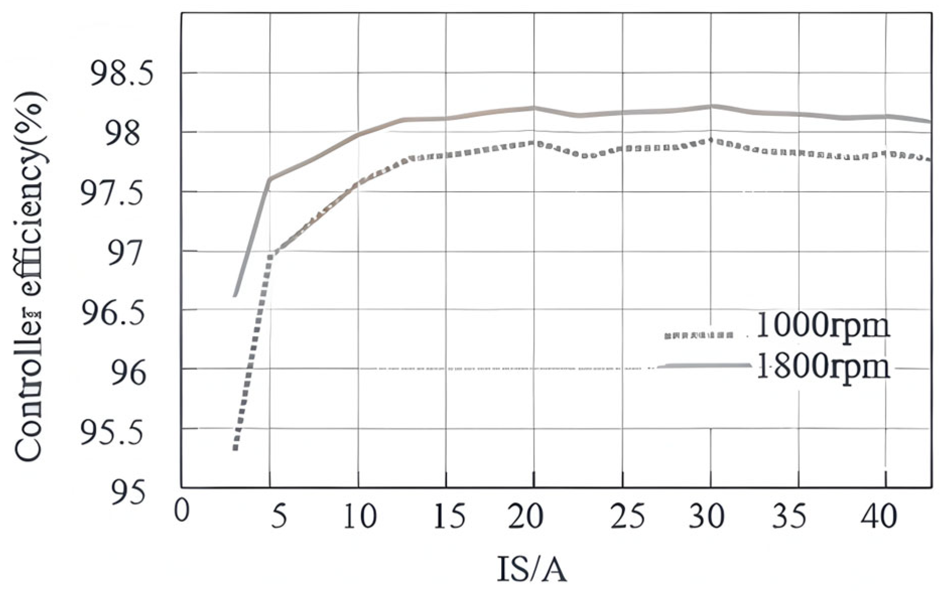
The efficiency curves of the controller were measured under conditions comprising a 600 V bus voltage and a 50 kHz switching frequency, at rotational speeds of 1000 rpm and 1800 rpm, with varying peak currents ranging from 0 to 40 A, as illustrated in Figure 39. The controller achieved a maximum efficiency of 98.2%, demonstrating its exceptional performance across different rotational speeds and power levels and confirming its capability for efficient operation.
Table 5 shows the data analysis results obtained from the controller during four long-term experiments. Based on the rotational speed, current, and controller temperature data from four experiments, the mean values, variances, and confidence intervals were calculated, respectively. The data show that the controller can be repeatedly used for long-term experiments without any failures, indicating high reliability.
Table 6 presents a performance comparison between the developed SiC controller and those created by leading enterprises in recent years. When compared to the SiC controller from Beijing Automotive New Energy Co., Ltd. of China and that from Fudi Power Company in Shenzhen, Guangdong Province of China, the switching frequency of this controller is higher than that for the controllers obtained from either company, and the efficiency of the controller is only 1% lower.

4. Conclusions

This paper presents the design of a motor controller featuring a high switching frequency utilizing discrete SiC MOSFET components. To attain the desired high switching frequency while minimizing current oscillation and voltage overshoot, a novel electronic system architecture is proposed. Additionally, a passive drive circuit is designed that effectively suppresses gate oscillation without the need for an additional control circuit. Furthermore, a new laminated stack PCB bus is implemented using advanced wiring technology, which offers low parasitic inductance, high current conduction capacity, and efficient heat dissipation. The controller successfully passed the dual-pulse and power tests, demonstrating stable operation over extended periods at a switching frequency of 50 kHz. It exhibits excellent electromagnetic compatibility, achieving a system efficiency of up to 98.2% and a power-to-weight ratio of 9 kW/kg. Additionally, the controller features a highly integrated electrical architecture, which includes integrated capacitors, AC/DC interfaces, and a PCB bus design. This design significantly reduces costs, simplifies assembly, and enhances production efficiency. However, this controller is still in the prototype stage and has not yet completed the necessary electromagnetic compatibility tests. Although the controller’s power is only 10 kW, different power levels can be achieved by paralleling multiple power modules. The proposed driving circuit method and the vertical multi-loop bus approach are applicable for implementing controllers of various power ratings. For heat dissipation in high-power controllers, a micro-channel liquid cooling system can be employed. Additionally, for electromagnetic interference (EMI) mitigation, filter design parameters can be optimized through simulation. Additionally, due to the limited execution cycle of the main control chip, higher switching frequency tests have not been conducted. Compared to the controllers produced by Beijing Automotive New Energy Vehicle Co., Ltd. and Feidi Electric Power Co., Ltd., its power density requires further enhancement.
The next steps will involve integrating firmware and incorporating health management functions—such as fault prediction and fault diagnosis—into the controller. Additionally, in-depth research will be conducted to enhance the electronic system’s power density, followed by completing related tests, including electromagnetic compatibility certification.

Author Contributions

Conceptualization, S.Z. and W.S.; methodology, S.Z.; validation, S.Z.; writing—review and editing, J.G.; supervision, J.G.; project administration. All authors have read and agreed to the published version of the manuscript.

Funding

This work was supported by National Key R&D Program of China, grant number 2021YFB2500600; National Key Research and Development Program of China during the 14th Five-Year Plan, grant number 2022YFB2502800.

Data Availability Statement

The original contributions presented in the study are included in the article, further inquiries can be directed to the corresponding author.

Conflicts of Interest

The authors declare no conflicts of interest.

Appendix A

The formula for determining the impedance of the magnetic beads is as follows.
The impedance of the magnetic bead is measured at a frequency of 100 MHz. Consequently, the impedance value is related to the inductance, according to Formula (A1). In the formula, L CB represents the inductance of the magnetic bead, and Z CB represents the impedance value of the magnetic bead.
L CB = Z CB 2 π × 100 × 10 6 = Z CB 628 × 10 6 ( H )
The inductor L CB , the total gate drive resistance R G , and the MOSFET gate input capacitance C in form an RLC series second-order system. The transfer function of the second-order system’s step response is
s 2 + R G L CB s + 1 L CB C in = 0
The system damping coefficient is ξ , and it satisfies
ξ = 1 2 R G C in L C B
According to control theory, the step response time of a second-order system is affected by the damping coefficient. In underdamped systems, in order to ensure the dynamic performance of the system, it is usually taken as ξ = 0.4 ~ 0.8 .
From this, we can conclude that
R G 2 C in 4 × ( 0.8 ) 2 < L CB < R G 2 C in 4 × ( 0.4 ) 2
The total driving resistance R G value of each MOSFET tube in the circuit is the same, and its value is 3 Ω. C in is the input capacitance of the MOSFET, and its value is 6 nF. From Formulas (6) and (9), we can obtain
13 Ω < Z CB < 53 Ω

References

  1. Liu, P.; Chen, Z.; Miao, Y. SiC MOSFET Active Driving Circuit Based on Switch Transient Feedback. J. Electr. Eng. 2022, 37, 4446–4457. [Google Scholar]
  2. Li, X.; Luo, Y.; Shi, Z. An Enhanced Circuit Model for SiC MOSFETs Based on Physics. J. Electr. Eng. 2022, 37, 5214–5226. [Google Scholar]
  3. Liu, B.; Liu, W.; Dong, K. Analytical Calculation Method for Stray Inductance of Converter Busbars Based on All Silicon Carbide Power Modules. J. Electr. Technol. 2021, 36, 2105–2114. [Google Scholar]
  4. Chen, J.; Deng, E.; Zhao, Z. Failure mechanism analysis of SiC MOSFET under different aging test methods. Trans. China Electrotech. Soc. 2020, 35, 5105–5114. [Google Scholar]
  5. Wang, L.; Zhao, C.; Zhang, T. Review of packaging technology for silicon carbide power modules. Trans. China Electrotech. Soc. 2023, 38, 4947–4962. [Google Scholar]
  6. Zou, M.; Zeng, Z.; Sun, P. Coordinated switching trajectory regulation of SiC device using variable resistance gate driver. Trans. China Electrotech. Soc. 2023, 38, 4286–4300. [Google Scholar]
  7. Chen, F.; Lee, S.; Jahns, T.M.; Sarlioglu, B. Comparative Investigation of Current-Source Inverters using SiC Discrete Devices and Power Modules. In Proceedings of the 2022 IEEE 9th Workshop on Wide Bandgap Power Devices & Applications (WiPDA), Redondo Beach, CA, USA, 7–9 November 2022; pp. 215–220. [Google Scholar]
  8. Liu, B.; Li, W.; Meng, D. Low-Stray Inductance Optimized Design for the Power Circuit of SiC-MOSFET-Based Inverters. IEEE Access 2020, 8, 20749–20758. [Google Scholar] [CrossRef]
  9. Li, Q.; Yang, Y.; Wen, Y.; Zhang, G.; Xing, W. Active Gate Driver With the Independent Suppression of Overshoot and Oscillation for SiC MOSFET Modules. IEEE Trans. Ind. Electron. 2025, 72, 2325–2335. [Google Scholar] [CrossRef]
  10. Shao, T.; Zheng, T.; Li, Z. SiC MOSFET Gate Driver Design Based on Interference Dynamic Response Mechanism. Trans. China Electrotech. Soc. 2021, 36, 4204–4214. [Google Scholar]
  11. Wang, N.; Zhang, J. Review of active gate driver for SiC MOSFET with switching trajectory optimization. Trans. China Electrotech. Soc. 2022, 37, 2523–2537. [Google Scholar]
  12. Ling, Y.; Zhao, Z.; Ji, S. Self-regulating control of IGBT switching characteristics with active gate drive. Trans. China Electrotech. Soc. 2021, 36, 2482–2494. [Google Scholar]
  13. Yue, Q.; Peng, H.; Tong, Q.; Kang, Y. A Novel Driving Current Control Approach in Enhanced Current-Source Gate Driver. IEEE Trans. Power Electron. 2023, 38, 10563–10568. [Google Scholar] [CrossRef]
  14. Zhao, S.; Zhao, X.; Wei, Y. A review of switching slew rate control for silicon carbide devices using active gate drivers. IEEE J. Emerg. Sel. Top. Power Electron. 2021, 9, 4096–4114. [Google Scholar] [CrossRef]
  15. Li, Z.; Chai, J.; Lu, H.; Li, Y. An Active Gate Driver for Suppressing the Current Oscillation of SiC MOSFET. In Proceedings of the 2021 IEEE 4th International Electrical and Energy Conference (CIEEC), Wuhan, China, 28–30 May 2021; pp. 1–5. [Google Scholar]
  16. Zhao, S.; Dearien, A.; Wu, Y. Adaptive multi-level active gate drivers for SiC power devices. IEEE Trans. Power Electron. 2020, 35, 1882–1898. [Google Scholar] [CrossRef]
  17. Yang, Y.; Wen, Y.; Gao, Y. Active gate driver for improving current sharing performance of paralleled high power SiC MOSFET modules. IEEE Trans. Power Electron. 2021, 36, 1491–1505. [Google Scholar]
  18. Sukhatme, Y.; Miryala, V.; Ganesan, P. Digitally controlled gate current source-based active gate driver for silicon carbide MOSFETs. IEEE Trans. Ind. Electron. 2020, 67, 10121–10133. [Google Scholar] [CrossRef]
  19. Lu, Y.; Yao, W. An Active Gate Driver Design to Reduce Voltage and Current Overshoots for SiC MOSFET Modules. In Proceedings of the 2020 IEEE 9th International Power Electronics and Motion Control Conference (IPEMC2020-ECCE Asia), Nanjing, China, 29 November–2 December 2020; pp. 915–920. [Google Scholar]
  20. Zhao, D.; Qiu, J.; Wang, P.; Wang, W. Active Gate Drive Circuit with Auxiliary Drive Branch for SiC MOSFET. In Proceedings of the 2022 25th International Conference on Electrical Machines and Systems (ICEMS), Chiang Mai, Thailand, 29 November–2 December 2022; pp. 1–5. [Google Scholar]
  21. Wang, Z.; Wu, Y.; Mahmud, M.H.; Yuan, Z.; Zhao, Y.; Mantooth, H.A. Busbar Design and Optimization for Voltage Overshoot Mitigation of a Silicon Carbide High-Power Three-Phase T-Type Inverter. IEEE Trans. Power Electron. 2021, 36, 204–214. [Google Scholar] [CrossRef]
  22. Zhu, J.; Yuan, J.; Nie, Z. Optimum design of planer busbar based on all-silicon carbide power module. Proc. CSEE 2019, 39, 6383–6393. [Google Scholar]
  23. Mirdoddi, K.; Nag, S.S. A Vertically Stacked Bus-bar Design Approach for Equal Power Loop Inductance in Three—Phase Voltage Source Inverter. In Proceedings of the 2023 IEEE Transportation Electrification Conference & Expo (ITEC), Chiang Mai, Thailand, 28 November–1 December 2023; pp. 1–5. [Google Scholar]
  24. Li, C.; Liu, B.; Zhu, Q.; Qi, Y.; Cao, J.; Du, Y.; Jain, P.; Song, G. Comparative Study on Stray Inductance and Current Sharing of a 90kW Inverter Using Multiple Discrete IGBT Devices in Parallel. In Proceedings of the 2024 IEEE 2nd International Conference on Power Science and Technology (ICPST), Dali, China, 9–11 May 2024; pp. 135–140. [Google Scholar]
  25. Ou, H.; Li, B.; Fang, X. Analysis of Switching Oscillation for Different Packaging Structures of SiC MOSFETs. Power Electron. Technol. 2024, 58, 138–140. [Google Scholar]
  26. Solero, L.; Serrao, V.; Taglioni, P. Low-voltage power electronics building block for automotive applications. In Proceedings of the Twenty-First Annual IEEE Applied Power Electronics Conference and Exposition, Dallas, TX, USA, 19–23 March 2006; pp. 633–639. [Google Scholar]
  27. Xin, D.; Huo, Y.; Wang, Q. Development of a compact 60kW three-phase asymmetry half-bridge power convertor with specifically designed busbar for switched reluctance machines. In Proceedings of the 2015 IEEE NW Russia Young Research in Electrical and Electronic Engineering Conference, St. Petersburg, Russia, 2–4 February 2015; pp. 311–316. [Google Scholar]
  28. Guler, N.; Ben Hazem, Z. A K-Additive Fuzzy Logic Approach for Optimizing FCS Sizing and Enhanced User Satisfaction. World Electr. Veh. J. 2024, 15, 150. [Google Scholar] [CrossRef]
  29. Ben Hazem, Z. Study of Q-learning and deep Q-network learning control for a rotary inverted pendulum system. Discov. Appl. Sci. 2024, 6, 49. [Google Scholar] [CrossRef]
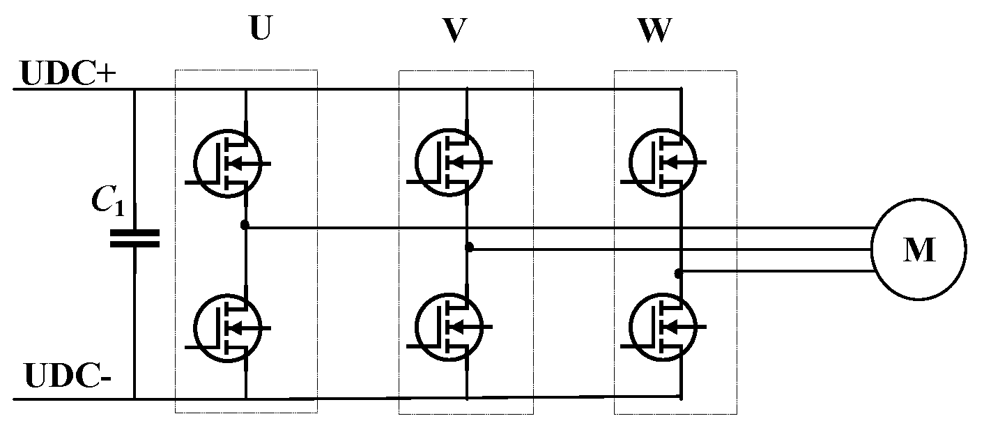
Figure 1. The schematic diagram of the main circuit of the controller.
Wevj 16 00474 g001
Figure 2. The controller electronic system structure diagram.
Wevj 16 00474 g002
Figure 3. The electrical structure layout of the controller.
Wevj 16 00474 g003
Figure 4. The principal block diagram of drive circuit.
Wevj 16 00474 g004
Figure 5. The curve of ferrite bead frequency vs. impedance.
Wevj 16 00474 g005
Figure 6. The crosstalk suppression principle.
Wevj 16 00474 g006
Figure 7. The decoupling design of PCB.
Wevj 16 00474 g007
Figure 8. The PCB layout diagram of driver board.
Wevj 16 00474 g008
Figure 9. The structure diagram of PCB busbar.
Wevj 16 00474 g009
Figure 10. The physical diagram of PCB busbar.
Wevj 16 00474 g010
Figure 11. The inductive model of the capacitor at different positions on the busbar. (a) The capacitor is located on one side of the busbar; (b) the capacitor is located in the middle position of the busbar.
Wevj 16 00474 g011
Figure 12. The parallel current equivalent circuit.
Wevj 16 00474 g012
Figure 13. The schematic diagram of low inductance stacked busbar structure.
Wevj 16 00474 g013
Figure 14. The current flow direction of common PCB stacked busbars.
Wevj 16 00474 g014
Figure 15. The current flow direction of the vertical double-layered looped busbar.
Wevj 16 00474 g015
Figure 16. The inductance diagram of dual-pulse circuit.
Wevj 16 00474 g016
Figure 17. The waveform of the turn-off time in the dual-pulse experiment under the 600 V/68 A.
Wevj 16 00474 g017
Figure 18. The simulation diagram of the busbar in Q3D.
Wevj 16 00474 g018
Figure 19. The design of controller heat dissipation structure.
Wevj 16 00474 g019
Figure 20. The heat dissipation path of power module.
Wevj 16 00474 g020
Figure 21. The block diagram of control algorithm.
Wevj 16 00474 g021
Figure 22. The block diagram of protection algorithm.
Wevj 16 00474 g022
Figure 23. The block diagram of CAN circuit.
Wevj 16 00474 g023
Figure 24. The filtering circuit of low-voltage power supply.
Wevj 16 00474 g024
Figure 25. The simulation circuit. (a) The simulation of differential-mode insertion loss; (b) the simulation of common-mode insertion loss.
Wevj 16 00474 g025
Figure 26. The results of simulation. (a) The simulation results of differential-mode insertion loss; (b) the simulation results of common-mode insertion loss.
Wevj 16 00474 g026
Figure 27. The prototype of discrete device parallel controller.
Wevj 16 00474 g027
Figure 28. The dual-pulse experimental platform.
Wevj 16 00474 g028
Figure 29. The dual-pulse test circuit diagram.
Wevj 16 00474 g029
Figure 30. The dual-pulse test waveform of 600 V/68 A.
Wevj 16 00474 g030
Figure 31. The dual-pulse test waveform of 600 V/68 A under the conventional drive circuit.
Wevj 16 00474 g031
Figure 32. The controller power experimental platform.
Wevj 16 00474 g032
Figure 33. The experimental waveforms at different rotational speeds and power levels. (a) Speed and current curve; (b) speed–torque curve.
Wevj 16 00474 g033
Figure 34. The test data of 600 V/10 kW.
Wevj 16 00474 g034
Figure 35. The temperature distribution map of the PCB bus board.
Wevj 16 00474 g035
Figure 36. Data waveforms obtained during the long-term test. (a) Current waveform under long-term operating conditions; (b) speed and torque waveform under long-term operating conditions; (c) temperature waveform of the controller shell under long-term operating conditions.
Wevj 16 00474 g036
Figure 37. The steady-state current waveform at a peak current of 36 A.
Wevj 16 00474 g037
Figure 38. The power generation voltage of load-end.
Wevj 16 00474 g038
Figure 39. The efficiency curve of the controller.
Wevj 16 00474 g039
Table 1. Inductance of each part of the circuit.
L loop (nH) L d /(nH) L P /(nH) L DC /(nH)Range of Temperature Increase (°C)Error Range (%)
Trial value45151515−10~50<5%
Table 2. Comparison of experimental and simulated values of the busbar inductance.
Name L DC /(nH)Error Range(%)
Trial value15<5%
Q3D simulation value of the vertical multi-loop busbar structure17<5%
Q3D simulation value of the single-loop busbar structure29<5%
Table 3. Comparison of busbar inductance values with those in the reference literature.
NameReference [21]/(nH)Reference [22]/(nH)Reference [23]/(nH)In this paper/(nH)
Inductance of Busbar 2714.913.715
Table 4. Thermal resistance distribution of power module heat dissipation.
NameMaterialThermal
Conductivity
(W/mK)
Thickness
(mm)
Thermal
Resistance
(K/W)
Module coating thermal resistance ------------0.27
Ceramic sheetAlumina29.30.60.05
Controller housingAluminum 60611675.20.08
Water channel shellAluminum 707513019.00.39
Thermal interface
Material
Silicone grease2.50.30.32
Convective heat transfer resistance------------0.40
Entire thermal resistance R j f ------------1.52
Table 5. The data analysis of long-term experiments.
ItemThe First
Experiment
The Second
Experiment
The Third
Experiment
The Fourth
Experiment
Mean ValueVarianceConfidence
Interval
Is(max)/A35.835.435.635.735.6250.021875[35.603, 35.646]
Speed/(r/min)99510011003998999.259.1875[990.24, 1008.2]
Controller
Temperature/(°C)
42404141410.5[40.51, 41.49]
Table 6. Comparison of controller indicators between this controller and that of other companies.
Pointer TypeSiC Controller of
BAIC New Energy Vehicle Co., Ltd.
SiC Controller of
Fudi Power Company
SiC Controller of
This Study
Switching frequency/Hz25<5050
Peak efficiency/%99.2%99.4%98.2%
Power density/(kW/L)434510
Disclaimer/Publisher’s Note: The statements, opinions and data contained in all publications are solely those of the individual author(s) and contributor(s) and not of MDPI and/or the editor(s). MDPI and/or the editor(s) disclaim responsibility for any injury to people or property resulting from any ideas, methods, instructions or products referred to in the content.