Article

Active Neutral-Point Voltage Balancing Strategy for Single-Phase Three-Level Converters in On-Board V2G Chargers

School of Electronic and Information Engineering, Chongqing Three Gorges University, Chongqing 404100, China
*
Author to whom correspondence should be addressed.
World Electr. Veh. J. 2025, 16(7), 406; https://doi.org/10.3390/wevj16070406
Submission received: 16 June 2025 / Revised: 10 July 2025 / Accepted: 20 July 2025 / Published: 21 July 2025

Abstract

Driven by the rapid advancement of Vehicle-to-Grid (V2G) and Grid-to-Vehicle (G2V) technologies, improving power quality and system stability during charging and discharging has become a research focus. To address this, this paper proposes a Model Predictive Control (MPC) strategy for Active Neutral-Point Voltage Balancing (ANPVB) in a single-phase three-level converter used in on-board V2G chargers. Traditional converters rely on passive balancing using redundant vectors, which cannot ensure neutral-point (NP) voltage stability under sudden load changes or frequent power fluctuations. To solve this issue, an auxiliary leg is introduced into the converter topology to actively regulate the NP voltage. The proposed method avoids complex algorithm design and weighting factor tuning, simplifying control implementation while improving voltage balancing and dynamic response. The results show that the proposed Model Predictive Current Control-based ANPVB (MPCC-ANPVB) and Model Predictive Direct Power Control-based ANPVB (MPDPC-ANPVB) strategies maintain the NP voltage within ±0.7 V, achieve accurate power tracking within 50 ms, and reduce the total harmonic distortion of current (THDi) to below 1.89%. The proposed strategies are tested in both V2G and G2V modes, confirming improved power quality, better voltage balance, and enhanced dynamic response.

1. Introduction

With the global transition of energy structures and growing awareness of environmental protection, electric vehicles (EVs) have become an innovative alternative to traditional fuel vehicles. According to the Global EV Outlook 2025 released by the International Energy Agency (IEA) [1], global electric car sales exceeded 17 million in 2024, accounting for more than 20% of new vehicle sales. China remains the largest market, contributing over 60% of global EV sales and hosting around 65% of public charging points. In contrast, growth in Europe and the United States has slowed due to reduced subsidies and unchanged emissions targets. These trends highlight the increasing importance of EV infrastructure. As the interface between EVs and the grid, the on-board charger (OBC) plays a critical role in determining charging efficiency and system reliability. It is responsible for converting grid-side alternating current (AC) into direct current (DC) suitable for charging the traction battery, and has thus become a major focus of ongoing research.
The OBC mainly consists of a front-stage AC/DC conversion and a rear-stage DC/DC conversion [2]. The front-stage AC/DC circuit performs power factor correction (PFC) and voltage conversion. It ensures that the input current remains synchronized with the grid voltage and reduces harmonic pollution to the grid. The rear-stage DC/DC circuit adjusts the DC voltage from the front stage to match the needs of the battery. It also provides electrical isolation and charging control. With the deep integration of smart grids and electric vehicles, OBCs are shifting from unidirectional charging to bidirectional energy exchange. V2G refers to discharging energy from the EV battery back to the grid to support peak shaving and frequency regulation. G2V represents the conventional charging process from the grid to the vehicle. These bidirectional energy flow modes place stricter requirements on the front-end converter of the OBC. First, the bidirectional flow of energy requires the converter to support power transfer in both directions. Second, grid connection standards require high-quality current waveforms and good PFC performance from the converter [3].
Compared with traditional two-level topologies, multilevel topologies, especially three-level topologies, have clear advantages. The total DC bus voltage is divided among multiple switching devices. This division reduces the voltage stress and the voltage change rate on each device. As a result, harmonic generation decreases, and the cost of passive filters is lowered [4,5]. At the same time, the three-level structure produces lower output voltage distortion. It also improves the THDi, enhancing overall power quality.
Although the three-level topology has many advantages, some problems still remain. First, it needs more power semiconductor devices, which increases the cost. Second, because the DC link is split, the NP voltage imbalance can degrade system performance. If a voltage imbalance occurs between the upper and lower DC-link capacitors, the output voltage waveform becomes distorted. Extra harmonic components may appear. Some devices may be exposed to excessive voltage stress. These problems reduce system efficiency and reliability [6].
The control strategy plays an important role in both V2G and G2V modes [7]. There are many control strategies for single-phase converters. Proportional-Integral (PI) control is a commonly used method. However, when the grid frequency drifts, tracking error increases, especially under dynamic scheduling in V2G applications [8]. Proportional-Resonant (PR) control may increase noise peaks in the system’s output spectrum. This often makes it difficult to meet grid connection standards [9,10]. Repetitive control is a steady-state control method derived from the internal model principle, enabling the output waveform to accurately follow the periodic reference signal. However, its main drawback is slow dynamic response. These methods are often not suitable for complex power electronic systems with multiple variables and constraints [11]. Super-Twisting Sliding Mode Control offers fast response and strong disturbance rejection. However, it requires many parameters and repeated trial-and-error tuning [12,13]. In recent years, MPC has been widely studied in the field of power electronics. As a feedforward optimization control method, it can achieve multi-objective control while meeting system constraints [14]. To address the NP voltage balancing problem, an effective method is to embed proper weighting factors into the cost function [15].
Although MPC provides multi-objective optimization capability, the selection of multiple weighting factors and its stability analysis still involve many uncertainties. In most cases, weighting factors are selected based on experience [16,17], yet they play a critical role in shaping the performance of power electronic controllers. Therefore, eliminating weighting factors entirely is a better way to reduce their influence on the control system. Reference [18] determines the voltage imbalance by evaluating the output current tracking error, which avoids directly sampling the voltages of the two capacitors. This reduces system cost and complexity. However, it may be difficult to detect faults in time if components fail. Reference [19] presents a sliding mode control approach that independently regulates the capacitor voltage and inductor current to their respective reference values, thus eliminating the need for weighting coefficients. However, this method is not suitable for single-phase three-level converters. Reference [20] avoids the use of weighting coefficients by forcing all control objectives to converge within a bounded invariant set. However, its strategy is too complex. These approaches focus solely on control methods and often involve complicated procedures.
To address this problem, a dedicated voltage balancing circuit can be added at the hardware level. Reference [21] proposed a voltage balancing circuit with flying capacitors for a diode-clamped five-level converter. This circuit achieved fast balancing of the DC-side capacitor voltages and stabilization of the NP voltage. However, its complex structure increases hardware cost, and the state machine control adds to the complexity of the control strategy. Some three-level inverter topologies inherently provide self-balancing of capacitor voltages. In the scheme of [22], a hybrid Cuk-Sepic DC-DC stage is used at the front end, which can automatically balance its two output voltages. As a result, the inverter’s performance is not affected by NP voltage imbalance. The approach in [23] uses a switched capacitor module, which connects split capacitors in parallel when outputting the semi-DC loop voltage to achieve voltage balancing. However, this method is only applicable to specific circuit topologies and lacks general applicability.
Traditional three-level converters rely on passive balancing strategies, which adjust the NP current direction by using the redundancy of switching vectors. However, this strategy is limited in effectiveness under the frequently changing load conditions typical of OBCs. To address this problem, this study proposes an improved solution by adding a third leg to the single-phase three-level topology. By actively controlling the third leg, the NP current can be directly regulated, thereby dispensing with the need for complex control algorithms and the use of weighting factors. This significantly enhances the stability and response speed of NP voltage balancing.
The remainder of this paper is organized as follows. Section 2 provides a detailed introduction to the mathematical model of the single-phase three-level topology. Section 3 discusses the mathematical model of the third leg and the active NP voltage balancing method. Section 4 verifies the proposed strategy through results and analysis. Section 5 presents the conclusion of this paper.

2. Mathematical Model

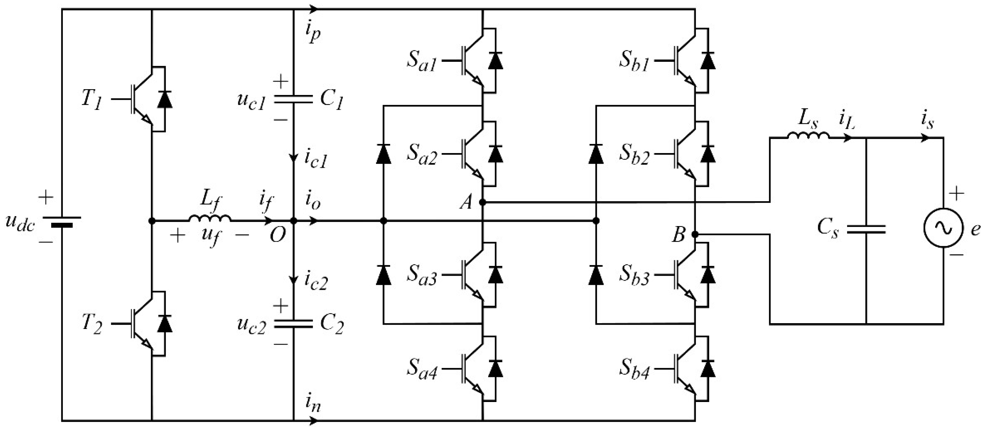
The topology of a single-phase three-level converter with three legs is illustrated in Figure 1. The variable u d c denotes the DC bus voltage on the EV side, which typically originates from the traction battery and the DC-DC converter. A current i f is injected into the midpoint of the DC bus via two power switches, T 1 and T 2 , and an inductor L f . This balancing leg is responsible for regulating or balancing the voltages U c 1 and U c 2 across the upper and lower DC bus capacitors, C 1 and C 2 , respectively. The central part of the circuit is a single-phase three-level converter composed of two bridge legs, A and B. The corresponding switching devices are S a 1 ~ S a 4 and S b 1 ~ S b 4 . The midpoint of the DC capacitors, denoted as point O , serves as the DC-side NP and enables three-level voltage output. On the AC side, the output is connected through an LC filter consisting of an inductor L s and capacitor C s , along with an AC voltage source e . The variables i L and i s represent the current through the filter inductor and the current on the AC side, respectively.
The single-phase three-level converter topology includes two main inverter legs. Each leg consists of four switching devices and two clamping diodes, and supports three distinct switching states, defined as S i { 1 , 0 , 1 } , where i { A , B } . The detailed switching combinations for each state are presented in Table 1.
Based on the defined switching states, a total of nine distinct voltage vectors can be derived for the converter. The converter’s operating characteristics corresponding to various switching states are summarized in Table 2.
Under ideal conditions, it is typically assumed that the voltages across the upper and lower DC-side capacitors, C 1 and C 2 , in a single-phase three-level converter, are balanced. However, in practical operation, these two voltages are often not exactly equal. As a result, based on the switching states shown in Table 2, the terminal voltages can be expressed as functions of the switching and the capacitor voltages, as given below
u a o = S a ( S a + 1 ) 2 u c 1 S a ( S a 1 ) 2 u c 2
u b o = S b ( S b + 1 ) 2 u c 1 S b ( S b 1 ) 2 u c 2
u a b = u a o u b o = S a ( S a + 1 ) 2 S b ( S b + 1 ) 2 u c 1 S a ( S a 1 ) 2 S b ( S b 1 ) 2 u c 2
The power switches are assumed to operate under ideal conditions. During the commutation process, all switching devices are considered free of switching losses and energy storage. Based on this assumption, the instantaneous power on the AC side and the DC side is considered balanced, leading to
u a b i L = i p u c 1 i n u c 2
i p represents the current flowing out of node p on the DC side, and i n denotes the current flowing out from node n on the DC side.
Substituting Equation (3) into Equation (4), the comparison yields
i p = S a ( S a + 1 ) S b ( S b + 1 ) 2 i L
i n = S a ( S a 1 ) S b ( S b 1 ) 2 i L
Applying Kirchhoff’s Current Law to the capacitors and their DC side gives the following equations
i o = ( i p + i n ) = ( S a 2 S b 2 ) i L

MPCC and MPPC Algorithms

In recent years, extensive research has been conducted on methods for generating virtual orthogonal components from single-phase signals. Common techniques include 90-degree phase shifting, the Hilbert transform, all-pass filters, and the Second-Order Generalized Integrator (SOGI) [24]. Among these, SOGI has emerged as a widely adopted method due to its structural simplicity, favorable dynamic characteristics, and strong capability to suppress harmonics and mitigate the effects of frequency deviations. Building upon this, the integration of SOGI with a Phase-Locked Loop (PLL) yields the SOGI-PLL structure, which further improves the accuracy of amplitude, phase, and frequency tracking. This configuration provides the necessary phase reference for implementing rotating coordinate transformations in single-phase systems [25].
As shown in Figure 2, the Second-Order Generalized Integrator (SOGI) processes the input signal x ( s ) through an internal structure of integrators and feedback, generating a quadrature signal x β ( s ) with a 90° phase shift and equal amplitude to the in-phase signal x α ( s ) . The corresponding transfer functions of the SOGI in the s-domain are given as follows
x α ( s ) = k ω n s s 2 + k ω n s + ω n 2 x ( s ) x β ( s ) = k ω n 2 s 2 + k ω n s + ω n 2 x ( s )
Here, ω n denotes the angular frequency of the fundamental grid voltage, and k is the gain coefficient used to adjust the filtering level and dynamic response characteristics of the system to the input signal.
As shown in Figure 1, applying Kirchhoff’s voltage law to analyze the voltage across the LC filter results in
L s d i L d t = u a b e R i L
By applying Equation (8) separately to the grid-side voltage e and the inductor current i L , the expressions for their rotating vectors of voltage and current are obtained as follows
e α = e = E cos ( ω t ) e β = E sin ( ω t )
i L α = I L cos ( ω t φ ) i L β = I L sin ( ω t φ )
In the above expressions, E and I L represent the peak values of the grid-side voltage and the inductor current of L s , respectively.
Substituting Equations (10) and (11) into Equation (9) yields
L s d i L α d t = u α R i L α e α L s d i L β d t = u β R i L β e β
After applying the Park transformation to the d-q rotating reference frame, the following expression is obtained
L s d i L d d t = u d e d R i L d + ω L s i L q L s d i L q d t = u q e q R i L q ω L s i L d
Let the sampling period be T s . By applying the forward Euler method to discretize (13), the MPCC expression can be obtained as follows
i L d ( k + 1 ) = T s L s u d ( k ) e d ( k ) + ω L s i L q ( k ) + 1 T s R L s i L d ( k ) i L q ( k + 1 ) = T s L s u q ( k ) e q ( k ) ω L s i L d ( k ) + 1 T s R L s i L q ( k )
Taking the leg current as the control target, the current cost function is defined as follows
J 1 = i L d r e f ( k + 1 ) i L d ( k + 1 ) 2 + i L q r e f ( k + 1 ) i L q ( k + 1 ) 2
Based on the instantaneous power theory, the instantaneous active power P and reactive power Q of the single-phase converter in the synchronous rotating d-q reference frame can be expressed as follows
P = 1 2 ( e d i L d + e q i L q ) Q = 1 2 ( e q i L d e d i L q )
When the d-axis of the synchronous rotating d-q reference frame is aligned with the grid voltage vector e , it follows that e d = E and e q = 0 . Under this condition, Equations (14) and (16) can be simplified as follows
i L d ( k + 1 ) = T s L s u d ( k ) E ( k ) + ω L s i L q ( k ) + 1 T s R L s i L d ( k ) i L q ( k + 1 ) = T s L s u q ( k ) ω L s i L d ( k ) + 1 T s R L s i L q ( k )
P = 1 2 E i L d Q = 1 2 E i L q
The differentials of P and Q are given by
d P d t = 1 2 E d i L d d t d Q d t = 1 2 E d i L q d t
Through the joint application of Equations (13), (18) and (19), the following expression is obtained
d P d t = 1 2 L s u d E 1 2 L s E 2 R L s P ω Q d Q d t = 1 2 L s E 2 R L s Q + ω P
Discretizing Equation (20) using the forward Euler approach yields the mathematical formulation of MPDPC as shown below
P ( k + 1 ) = T s 1 2 L s u d ( k ) E 1 2 L s E 2 ( k ) ω Q ( k ) + 1 T s R L s P ( k ) Q ( k + 1 ) = T s 1 2 L s E 2 ( k ) + ω P ( k ) + 1 T s R L s Q ( k )
Taking the grid-side power as the control objective, the power cost function is defined as follows
J 2 = P r e f ( k + 1 ) P ( k + 1 ) 2 + Q r e f ( k + 1 ) Q ( k + 1 ) 2

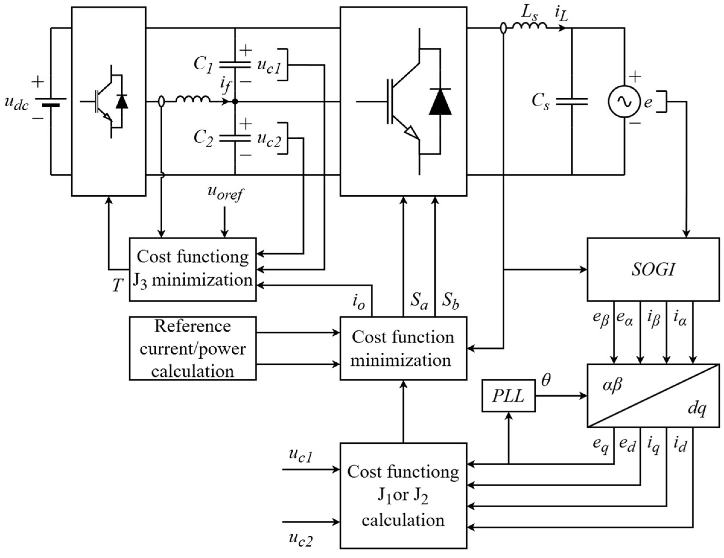
3. Model Predictive Control of Active NP Voltage Using the Third Leg

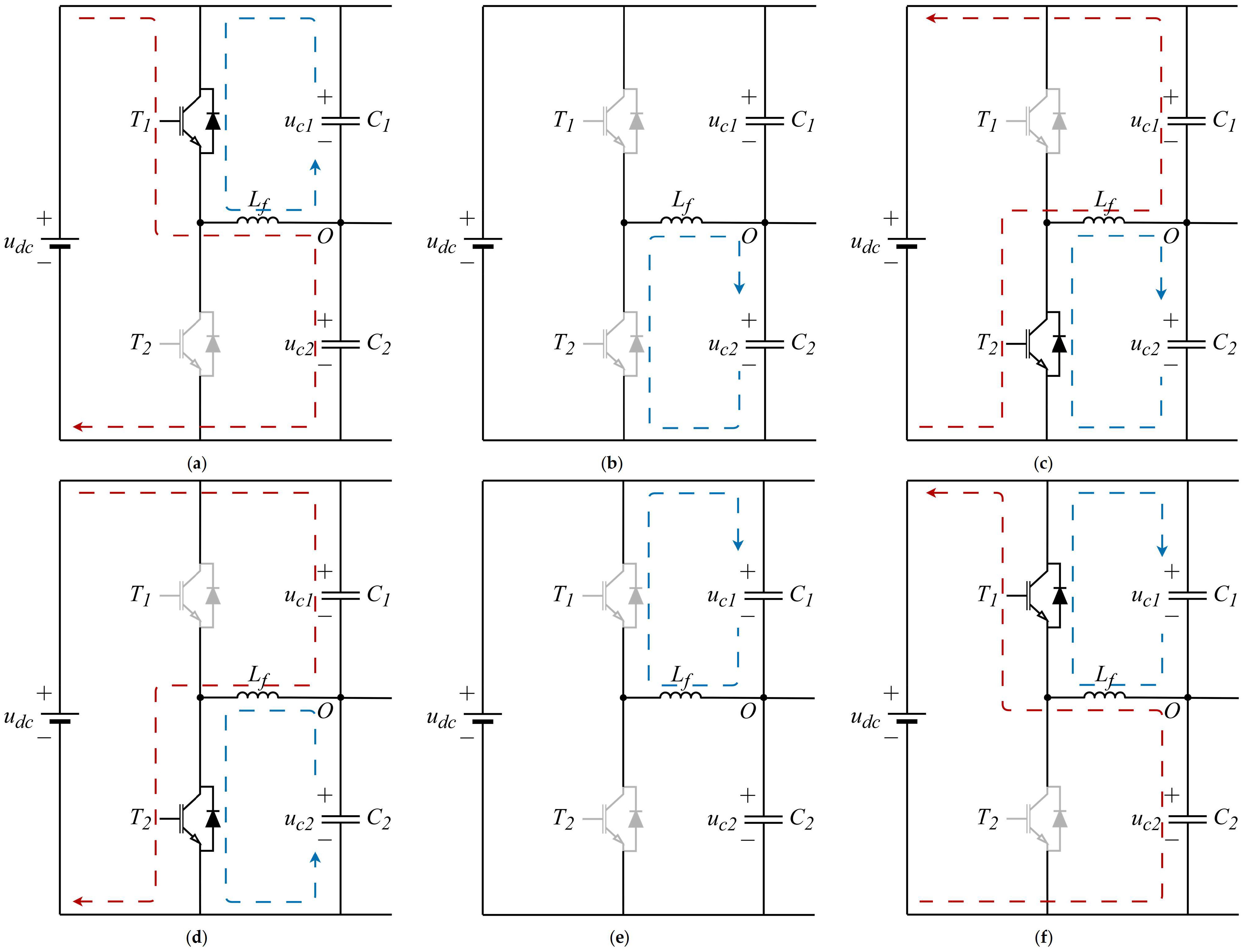
3.1. Operating Modes of the Third Leg

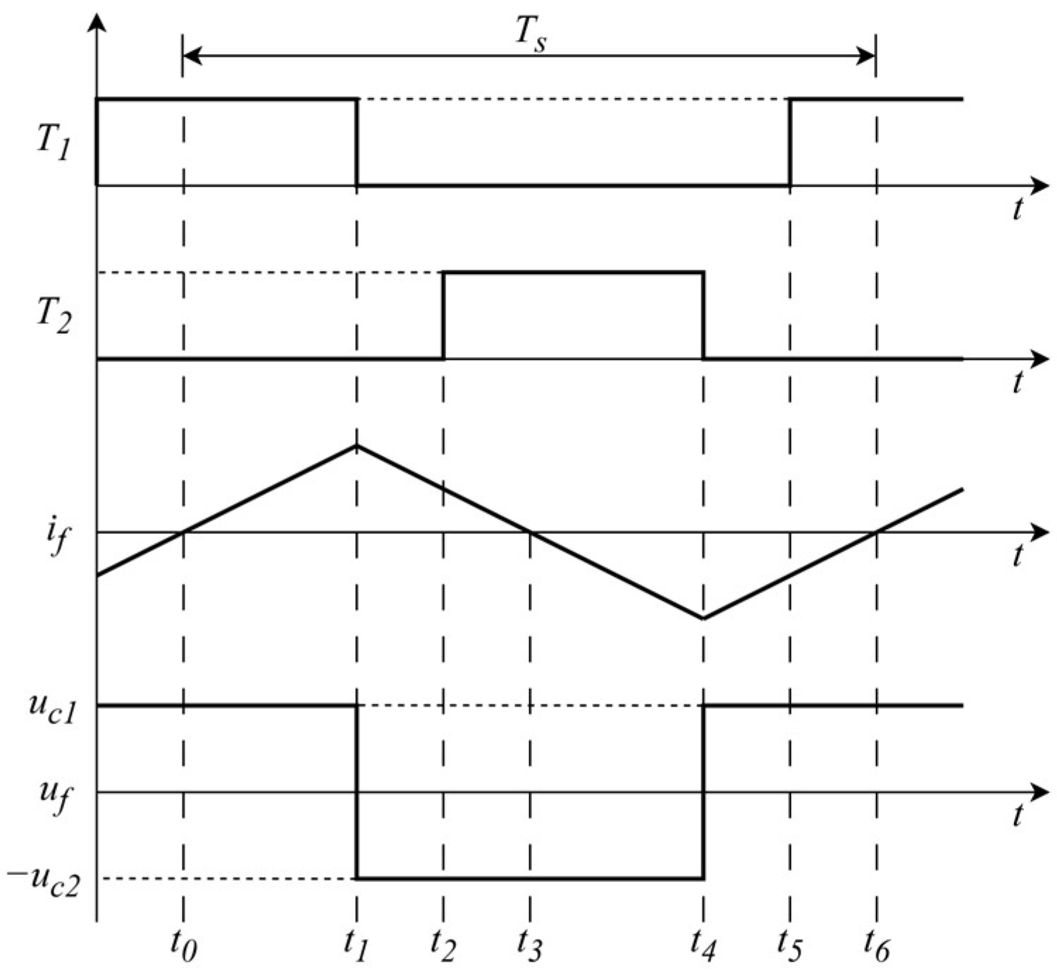
By controlling the switching devices of the third leg to turn on and off, appropriate charging strategies are applied to the upper and lower DC bus capacitors, enabling the balancing of the NP voltage. When the voltage across C 1 is higher, energy is transferred from C 1 to C 2 through the third leg; conversely, when the voltage across C 2 is higher, energy is transferred from C 2 to C 1 via the third leg, causing the voltage of C 1 to increase. Based on the switching states and the direction of the inductor current, there are six operating modes, as illustrated in Figure 3 and Figure 4.
Mode 1: T 1 is turned ON while T 2 is turned OFF. This mode corresponds to the interval t 0 t 1 . The current i f begins increasing from zero. A closed loop is formed by the DC bus voltage u d c , T 1 , L f , and C 2 , allowing the DC source to charge C 2 . Meanwhile, C 1 , T 1 , and L f form another loop where C 1 charges L f . The voltage across L f equals u c 1 , resulting in u c 1 decreasing and u c 2 increasing.
Mode 2: Both T 1 and T 2 are turned OFF during the interval t 1 t 2 . The current i f remains positive and flows through a loop formed by C 2 , T 2 , and L f . In this state, L f charges C 2 , with the voltage across L f being opposite to u c 2 . Voltage u c 2 increases.
Mode 3: T 1 is OFF and T 2 is ON in the interval t 2 t 3 . The current i f remains positive. A loop is formed by u d c , T 2 , L f , and C 1 , where C 1 supplies energy to the DC bus. Simultaneously, C 2 , T 2 , and L f form another loop that continues to charge C 2 . The voltage across L f is opposite to u c 2 , leading to a decrease in u c 1 and an increase in u c 2 .
Mode 4: During the interval t 3 t 4 , T 1 remains OFF and T 2 is ON. The current i f becomes negative. The loop formed by u d c , T 2 , L f , and C 1 allows the DC source to charge C 1 . Meanwhile, C 2 , T 2 , and L f form a loop where C 2 discharges into L f . The voltage across L f is opposite to u c 2 . As a result, u c 1 increases and u c 2 decreases.
Mode 5: Both T 1 and T 2 are OFF during the interval t 4 t 5 , and i f remains negative. A loop is formed by C 1 , T 1 , and L f , where L f charges C 1 . The voltage across L f equals u c 1 , resulting in an increase of u c 1 .
Mode 6: T 1 is ON and T 2 is OFF during the interval t 5 t 6 . The current i f remains negative. A loop formed by u d c , T 1 , L f , and C 2 allows C 2 to supply energy to the DC bus. At the same time, C 1 , T 1 , and L f form a loop, where L f continues to charge C 1 . The voltage across L f equals u c 1 , leading to an increase in u c 1 and a decrease in u c 2 .

3.2. Model Predictive Control of NP Voltage

Let the DC bus voltage be denoted as u d c , and the NP voltage difference as u o . Then, u d c and u o can be expressed as follows
u d c = u c 1 + u c 2 u o = u c 2 u c 1
The currents of the upper and lower capacitors on the DC bus can be expressed as
i c 1 = C 1 d 1 2 ( u d c u o ) d t i c 2 = C 2 d 1 2 ( u d c + u o ) d t
The designed circuit employs C 1 = C 2 = C . Based on Kirchhoff’s law, the circuit Equation for the third bridge arm is given by
i f i o = i c 2 i c 1 = C d u o d t
u f = L f d i f d t
By applying the forward Euler method to discretize Equations (25) and (26), the following expressions can be obtained
u o ( k + 1 ) = T s C i f ( k ) i o ( k ) + u o ( k )
i f ( k + 1 ) = T s L f u f ( k ) + i f ( k )
Equation (28) provides the required expression for model predictive NP voltage control. From Figure 3, along with Equations (27) and (28), it can be seen that u f is related to both the switching actions and i f . The value of i f at time step k + 1 depends on u f at time step k , while the predicted NP voltage difference u 0 at k + 1 depends on i f at k , and is therefore independent of u f at k . This indicates that Equation (27) alone cannot be used to control the NP voltage difference at k + 1 through the switching action at k . To resolve this problem, a two-step prediction method is employed. Applying the two-step prediction to Equation (27) yields the following
u o ( k + 2 ) = T s C i f ( k + 1 ) i o ( k + 1 ) + u o ( k + 1 )
By substituting Equations (27) and (28) into Equation (29), the following expression is obtained
u o ( k + 2 ) = T s C T s L f u f ( k ) + i f ( k ) i o ( k + 1 ) + T s C i f ( k ) - i o ( k ) + u o ( k )
Taking the capacitor voltage difference as the control objective, the DC bus voltage balancing cost function is defined as follows
J 3 = u o r e f ( k + 2 ) u o ( k + 2 ) 2
The above method provides a theoretical basis for controlling a single-phase three-level three-leg converter. However, in practice, MPC algorithms inherently suffer from delay issues. At the beginning of each sampling period, the processes of voltage and current sampling, reference acquisition, and the computational burden of the MPC algorithm consume significant processing time on the digital controller. This results in action delay, causing the predicted values to deviate from the reference values and degrading overall system performance. Therefore, delay compensation must be considered in the control algorithm. To mitigate this issue, this paper adopts a two-step prediction method to compensate for the delay-induced errors. The specific steps are as follows:
(1) Sample the controlled variables at time step k .
(2) Use the mathematical model to calculate the estimated values of i L d , i L q , e d , e q , i f , u o , P , and Q at time step k + 1 .
(3) Based on these estimates and the predictive model, calculate the predicted values of each voltage vector at time step k + 2 , namely
i L d ( k + 2 ) = T s L s u d ( k + 1 ) E ( k + 1 ) + ω L s i L q ( k + 1 ) + 1 T s R L s i L d ( k + 1 ) i L q ( k + 2 ) = T s L s u q ( k + 1 ) ω L s i L d ( k + 1 ) + 1 T s R L s i L q ( k + 1 )
P ( k + 2 ) = T s 1 2 L s u d ( k + 1 ) E ( k + 1 ) 1 2 L s E 2 ( k + 1 ) ω Q ( k + 1 ) + 1 T s R L s P ( k + 1 ) Q ( k + 2 ) = T s 1 2 L s E 2 ( k + 1 ) + ω P ( k + 1 ) + 1 T s R L s Q ( k + 1 )
Since the NP voltage difference at time step k + 2 cannot be controlled directly by the switching actions at k + 1 , it is necessary to predict the estimated value of u 0 at k + 2
u o ( k + 3 ) = T s C T s L f u f ( k + 1 ) + i f ( k + 1 ) i o ( k + 2 ) + T s C i f ( k + 1 ) - i o ( k + 1 ) + u o ( k + 1 )
At this point, the expressions of the cost functions are given by
J 1 = i L d r e f ( k + 2 ) i L d ( k + 2 ) 2 + i L q r e f ( k + 2 ) i L q ( k + 2 ) 2
J 2 = P r e f ( k + 2 ) P ( k + 2 ) 2 + Q r e f ( k + 2 ) Q ( k + 2 ) 2
J 3 = u o r e f ( k + 3 ) u o ( k + 3 ) 2
(4) Store the optimal predicted values, switching states, and i o , which will serve as input data for the next sampling period.
The configuration of the proposed predictive control strategy is shown in Figure 5.

4. Results and Analysis

4.1. Parameter Selection

According to Kirchhoff’s law, the current loop equation of the LC-type filter circuit can be expressed as
C s d e d t = i L i s
By combining Equations (9) and (38) and neglecting the grid-side load, the transfer function of the LC filter is obtained as
U C ( s ) U a b ( s ) = 1 L s C s s 2 + R C s s + 1 = ω L 2 s 2 + 2 ξ ω L s + ω L 2
The resonant angular frequency is given by ω L = 1 / L s C s , and the damping ratio is ξ = 1 / 2 R C s / L s . It can be observed that the system is a second-order oscillatory system, and its cutoff frequency is
f L = 1 2 π L s C s
The current ripple of the output filter determines the minimum inductance value. Typically, the ripple current is selected as 20% of the peak output current under rated operating conditions.
Δ I L max = 2 P max E / 2 × 20 % = 2 P max 5 E
Let Δ I L denote the inductor current ripple. According to Kirchhoff’s law, the ripple current across the inductor is given by
Δ I L = u d c e L s × D ( t ) f s
where D ( t ) is the duty cycle and f s is the switching frequency. Since the switching frequency is much higher than the grid frequency, it can be assumed that
e = D ( t ) u d c
Substituting (43) into (42) yields
Δ I L = D ( t ) D 2 ( t ) u d c f s L s
The ripple current reaches its maximum when D ( t ) = 0.5 , and can be expressed as
Δ I L max = u d c 4 f s L s
By combining (41) and(45), the minimum filter inductance is given by
L s min = 5 u d c E 8 f s P max
When the cutoff frequency is much lower than the switching frequency, harmonic suppression is most effective. Typically, the cutoff frequency f L of the LC filter is selected to be less than 1/10 of the switching frequency f s . According to Equation (40), the filter capacitance should satisfy the following condition
C s 1 L s 2 π f s × 1 10 2
According to the power conservation principle, the energy stored in the DC-link capacitor over one period is given by
W = P f
Let f denote the grid frequency. The energy supplied by the filter capacitor in each cycle is given by
W 2 = 2 × C 2 u d c 2 ( u d c Δ u ) 2
Here, Δ u represents the ripple amplitude of the DC bus voltage, generally taken as 5% of the DC bus voltage. By combining Equations (48) and (49), we obtain
C = P 2 f 2 u d c Δ u Δ u 2
The inductance of the third bridge leg can be designed with reference to the boost converter inductor. The inductance is calculated by the following formula
L f > D ( t ) 1 D ( t ) 2 u d c 2 T S η P
η is the current ripple coefficient, usually less than 1. When D ( t ) = 1 / 3 , the right-hand side of the equation reaches its maximum value, that is
L f > 4 u d c 2 T S 27 η P
To verify the effectiveness and superiority of the proposed MPC-ANPVB strategy for the single-phase three-level converter, a detailed simulation study was conducted. The simulation parameters are summarized in Table 3. The proposed method was compared with the conventional MPCC, MPDPC, and PI-ANPVB strategies. The simulations were carried out using MATLAB/Simulink R2023b.

4.2. Comparative Analysis of Control Strategies

In the experimental setup, the active power reference was 5 kW from 0 to 0.3 s and −5 kW from 0.3 to 0.5 s, while the reactive power reference remained at 0 Var throughout. NP voltage balancing was initiated at 0.1 s, and the system mode switched from V2G to G2V at 0.3 s. Performance comparisons of the five methods are presented in Figure 6, Figure 7 and Figure 8.
Figure 6 shows the active and reactive power response curves under the five control strategies. As shown in Figure 6a, after the NP voltage balancing was activated at 0.1 s, the conventional MPCC exhibited a transient deviation of approximately 100 W in active power, which quickly recovered within around 20 ms. In contrast, the other four strategies maintained smoother responses without significant fluctuation. For the reactive power in Figure 6b, a transient disturbance of about 33 Var was observed under conventional MPCC, while the other methods were nearly unaffected. During the mode transition at 0.3 s, all strategies exhibited some fluctuations in reactive power caused by the abrupt change in operating conditions, but the steady-state control performance remained unaffected.
Figure 7 illustrates the variations of the upper and lower DC-link capacitor voltages, u c 1 and u c 2 , under the five control strategies when NP balancing is activated at 0.1 s. As shown in Figure 7a,b, the conventional MPCC and MPDPC exhibit relatively slow recovery processes after NP balancing is triggered, and the voltage difference decreases at a slower rate. Figure 7c presents the results for the PI-ANPVB approach. Although it shows noticeable oscillations during the initial adjustment phase, the voltage difference between u c 1 and u c 2 decreases rapidly, and the total settling time is shorter than that of the traditional model predictive control methods. In Figure 7d,e, corresponding to MPCC-ANPVB and MPDPC-ANPVB, respectively, the capacitor voltages converge rapidly within a short time frame, with no observable oscillation and a smooth dynamic response. As shown in Figure 7f, the PI-based strategy exhibits a transient fluctuation in NP voltage at 0.1 s but restores balance within 4 ms. In contrast, MPCC and MPDPC take nearly 10 ms to gradually converge. By comparison, the two improved strategies based on ANPVB, namely MPCC-ANPVB and MPDPC-ANPVB, achieve near-complete voltage balance in approximately 2 ms without any significant oscillation, demonstrating faster regulation and superior voltage symmetry.
To further validate the performance of the proposed strategy, the grid currents under the five control methods are compared. The grid voltage and current waveforms are shown in Figure 8. In Figure 8a,b, corresponding to the V2G and G2V modes, respectively. In the V2G mode, the grid current remains in phase with the voltage waveform, while in the G2V mode, it is in antiphase, aligning with the power flow characteristics illustrated in Figure 6. Under the PI-ANPVB strategy, noticeable current ripples can be observed. At 0.1 s, NP voltage balancing is activated. As seen in Figure 8a, the current waveform under the conventional MPCC strategy exhibits significant distortion near 0.1 s.
To further evaluate waveform quality, the THDi was extracted and compared for the five control strategies. The results are summarized in Table 4. Under the V2G mode, the THDi values of the conventional MPCC and MPDPC strategies are 1.96%, and under the G2V mode, they are 2.08% and 2.05%, respectively, indicating relatively low current distortion. In contrast, the PI-ANPVB strategy exhibits increased THDi values of 4.76% and 4.78% in the two operating modes, significantly higher than those of the other methods. The two improved strategies, MPCC-ANPVB and MPDPC-ANPVB, demonstrate better current quality, with waveforms closer to the ideal sinusoid. Their THDi values remain below 1.89% in both operating modes.

4.3. Dynamic Performance Under Active Power Changes

The active power reference starts at 5000 W and decreases stepwise every 0.2 s to 3000 W, 0 W, −3000 W, and −5000 W, while the reactive power reference remains at 0 Var. The results of the improved strategy are shown in Figure 9. Current waveforms exhibit slight distortion at the initial stage and during active power step changes; however, these distortions are brief and rapidly recover, indicating good overall current quality. Regarding power response, active power closely follows the reference changes with smooth step transitions, minimal overshoot, and the steady-state control process completing within approximately 50 ms. Reactive power experiences transient fluctuations during power transitions, with fluctuation magnitude roughly proportional to the active power change; larger changes lead to more noticeable transient deviations, but most recover to near zero within 50 ms, meeting the system’s reactive power requirements. The upper and lower capacitor voltages remain symmetric throughout the power variation process without significant deviation or oscillation, with the amplified voltage waveform maintained within ±0.7 V.
To highlight the advantages of the proposed method, Table 5 compares it with several typical single-phase bidirectional AC/DC converters reported in the recent literature. The comparison covers control strategies, power ratings, charging levels, DC bus or battery voltages, circuit complexity, and performance indicators such as power factor (PF) and total harmonic distortion (THD).

4.4. Comparison

To further highlight the effectiveness of the proposed method, a comparison with several existing bidirectional converter solutions is provided. As shown in Table 5, most existing solutions adopt PI or PR control methods with relatively simple filter structures and low component counts. The proposed MPC-based strategy, despite a slightly more complex structure, achieves lower THD (1.89%) while maintaining a high PF of 0.99, demonstrating improved power quality. In addition, it supports SAE Level 1/2 charging with 5 kW output, making it suitable for mid-power V2G applications.

5. Conclusions

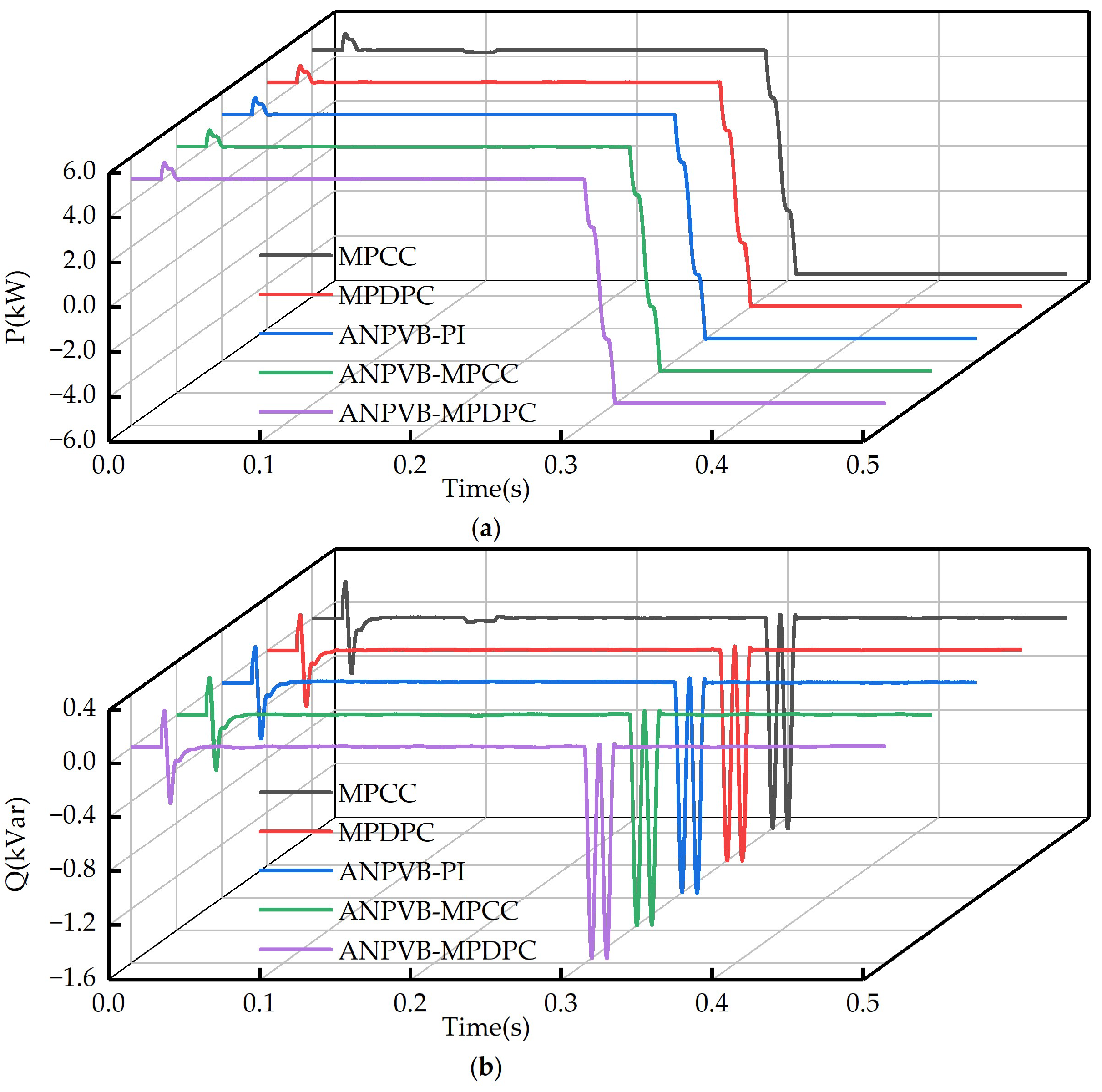
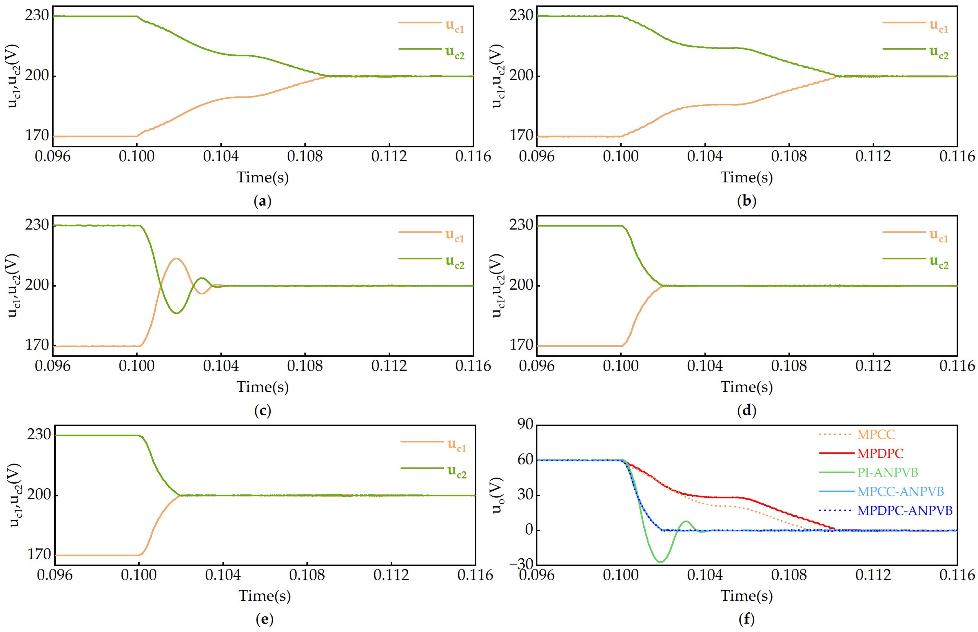
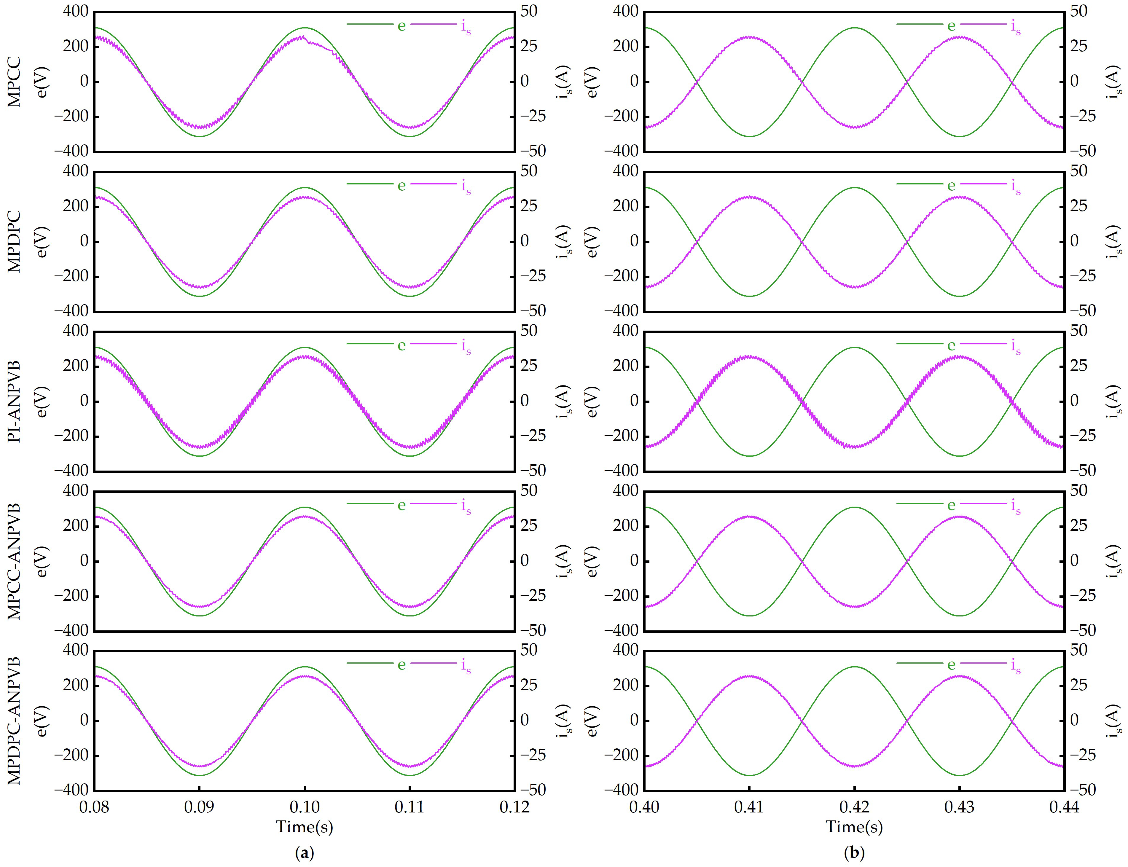
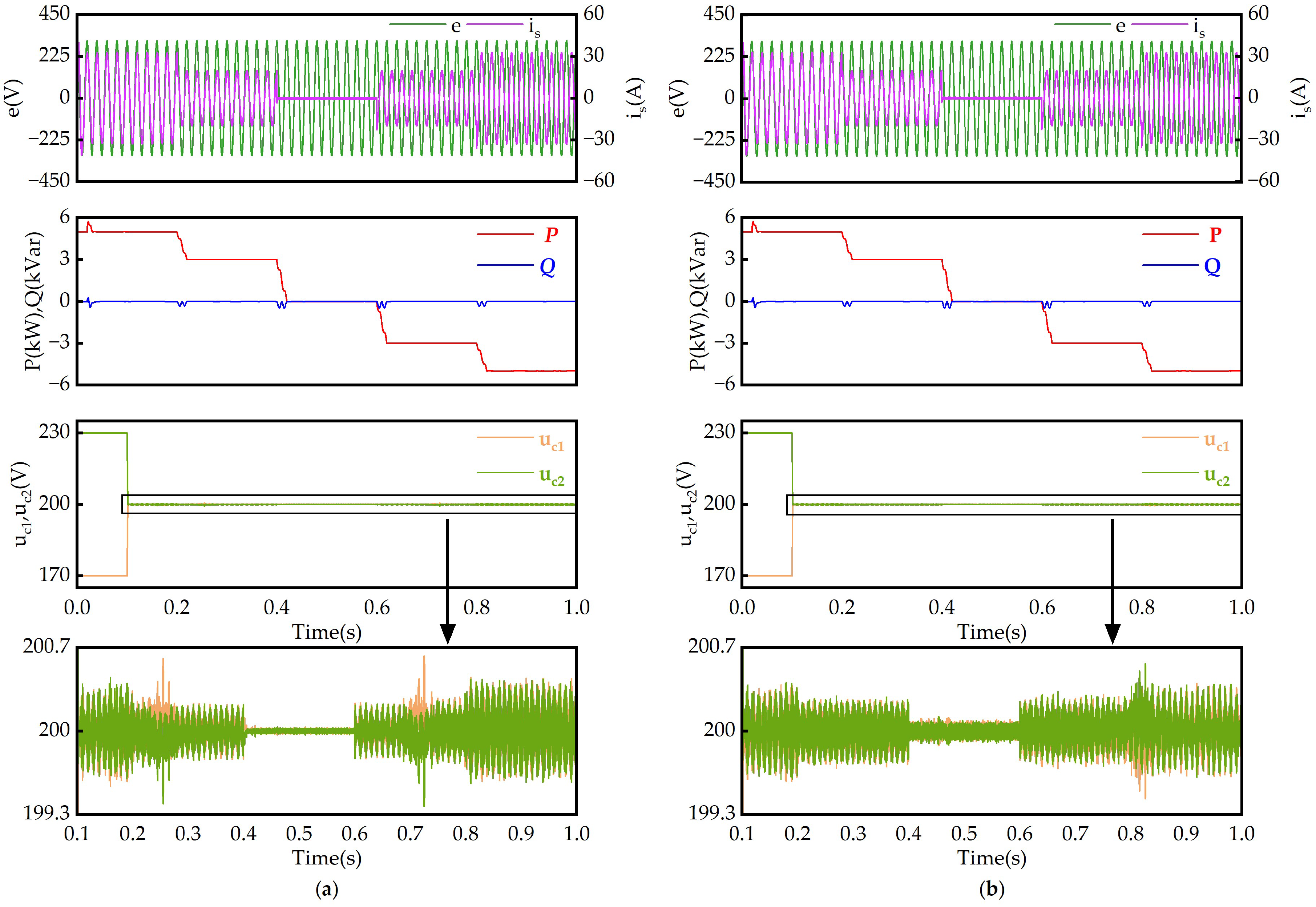
This paper proposed an improved model predictive control strategy integrating the hardware-based ANPVB for single-phase three-level converters in on-board V2G applications. Two approaches, MPCC-ANPVB and MPDPC-ANPVB, were developed and evaluated. The proposed methods effectively mitigate NP voltage imbalance without relying on weighting factor tuning. By directly adjusting the NP voltage via hardware, the control system is simplified, enhancing robustness and feasibility. Compared with conventional MPC and other existing methods reported in the literature, the improved strategies demonstrate faster and more stable balancing performance, maintaining better voltage symmetry across the DC-link capacitors under dynamic operating conditions. Simulation results under two key scenarios, bidirectional mode switching and active power step changes, show that MPCC-ANPVB and MPDPC-ANPVB maintain smoother current waveforms, lower current harmonic distortion, and accurate power tracking. Even during continuous step changes in active power reference, the NP voltage remains well balanced without significant deviation. In conclusion, the proposed control schemes enhance NP voltage regulation while ensuring high power quality and dynamic performance. These features make them suitable for practical V2G converter control applications. While the proposed control strategies have been validated through detailed simulation studies, practical implementation may encounter additional challenges such as measurement noise, parameter variation, and digital control delay. Therefore, future work will focus on building a hardware prototype platform to experimentally verify their effectiveness and robustness under realistic operating conditions.

Author Contributions

Conceptualization, Q.C. and Z.T.; methodology, Q.C. and Z.T.; software, Q.C. and B.X.; validation, Q.C., B.X. and L.Q.; formal analysis, Q.C. and Z.Z.; investigation, Q.C. and S.G.; resources, Q.C.; data curation, Q.C. and L.Q.; writing—original draft preparation, Q.C.; writing—review and editing, Q.C. and Z.T.; visualization, Q.C.; supervision, Z.T.; project administration, Q.C. All authors have read and agreed to the published version of the manuscript.

Funding

This research received no external funding.

Data Availability Statement

The original contributions presented in this study are included in the article, further inquiries can be directed to the corresponding author.

Conflicts of Interest

The authors declare no conflicts of interest.

References

  1. International Energy Agency (IEA). Global EV Outlook 2025; IEA: Paris, France, 2025; Available online: https://www.iea.org/reports/global-ev-outlook-2025 (accessed on 6 July 2025).
  2. Wouters, H.; Martinez, W. Bidirectional Onboard Chargers for Electric Vehicles: State-of-the-Art and Future Trends. IEEE Trans. Power Electron. 2024, 39, 693–716. [Google Scholar] [CrossRef]
  3. Khaligh, A.; D’Antonio, M. Global Trends in High-Power On-Board Chargers for Electric Vehicles. IEEE Trans. Veh. Technol. 2019, 68, 3306–3324. [Google Scholar] [CrossRef]
  4. Lee, H.-J.; Woo, T.; Kim, S.; Yoon, Y.-D. Improved Neutral-Point Voltage Balancing Control With Time Delay Compensation and Antiwindup Loop for a Three-Level NPC Inverter. IEEE Trans. Ind. Appl. 2021, 57, 4970–4980. [Google Scholar] [CrossRef]
  5. Zhang, G.; Liu, Q.; Wang, J.; Li, C.; Gu, X. Improved Model Predictive Current Control of NPC Three-Level Converter Fed PMSM System for Neutral Point Potential Imbalance Suppression. World Electr. Veh. J. 2022, 13, 113. [Google Scholar] [CrossRef]
  6. Zhang, X.; Ma, Z.; Niu, H.; Huang, J.; Lin, G. Finite-Control-Set Model-Predictive Control With Data-Driven Switching Frequency Control for Single-Phase Three-Level NPC Rectifiers. IEEE Trans. Ind. Electron. 2024, 71, 7180–7189. [Google Scholar] [CrossRef]
  7. Jaman, S.; Chakraborty, S.; Tran, D.-D.; Geury, T.; El Baghdadi, M.; Hegazy, O. Review on Integrated On-Board Charger-Traction Systems: V2G Topologies, Control Approaches, Standards and Power Density State-of-the-Art for Electric Vehicle. Energies 2022, 15, 5376. [Google Scholar] [CrossRef]
  8. Gehrke, B.S.; Jacobina, C.B.; Rezende de Sousa, R.P.; da Silva, I.R.F.M.P.; Méllo, J.P.R.A.; Brandão de Freitas, N. Single-Phase to Single-Phase Three-Wire Power Converters Based on Two-Level and Three-Level Legs. IEEE Trans. Ind. Appl. 2022, 58, 2291–2300. [Google Scholar] [CrossRef]
  9. Lin, B.; Peng, L.; Liu, X. Selective Pole Placement and Cancellation for Proportional–Resonant Control Design Used in Voltage Source Inverter. IEEE Trans. Power Electron. 2022, 37, 8921–8934. [Google Scholar] [CrossRef]
  10. Quan, X. Improved Dynamic Response Design for Proportional Resonant Control Applied to Three-Phase Grid-Forming Inverter. IEEE Trans. Ind. Electron. 2021, 68, 9919–9930. [Google Scholar] [CrossRef]
  11. Ye, J.; Liu, L.; Xu, J.; Shen, A. Frequency Adaptive Proportional-Repetitive Control for Grid-Connected Inverters. IEEE Trans. Ind. Electron. 2021, 68, 7965–7974. [Google Scholar] [CrossRef]
  12. Chai, J.; Wang, M.; Li, Z.; Xu, Z. Improved Super-Twisting Sliding Mode Control for Single-Phase T-Type Three-Level Converters Based on Fixed-Time Extended State Observer. IEEE Trans. Transp. Electrif. 2024, 10, 5307–5317. [Google Scholar] [CrossRef]
  13. Liu, J.; Shen, X.; Alcaide, A.M.; Yin, Y.; Leon, J.I.; Vazquez, S.; Wu, L.; Franquelo, L.G. Sliding Mode Control of Grid-Connected Neutral-Point-Clamped Converters Via High-Gain Observer. IEEE Trans. Ind. Electron. 2022, 69, 4010–4021. [Google Scholar] [CrossRef]
  14. Harbi, I.; Rodriguez, J.; Liegmann, E.; Makhamreh, H.; Heldwein, M.L.; Novak, M.; Rossi, M.; Abdelrahem, M.; Trabelsi, M.; Ahmed, M.; et al. Model-Predictive Control of Multilevel Inverters: Challenges, Recent Advances, and Trends. IEEE Trans. Power Electron. 2023, 38, 10845–10868. [Google Scholar] [CrossRef]
  15. Vazquez, S.; Aguilera, R.P.; Acuna, P.; Pou, J.; Leon, J.I.; Franquelo, L.G.; Agelidis, V.G. Model Predictive Control for Single-Phase NPC Converters Based on Optimal Switching Sequences. IEEE Trans. Ind. Electron. 2016, 63, 7533–7541. [Google Scholar] [CrossRef]
  16. Aguilera, R.P.; Quevedo, D.E. On Stability of Finite Control Set MPC Strategy for Multicell Converters. In Proceedings of the 2010 IEEE International Conference on Industrial Technology, Via del Mar, Chile, 14–17 March 2010; pp. 1277–1282. [Google Scholar]
  17. Cortes, P.; Kouro, S.; La Rocca, B.; Vargas, R.; Rodriguez, J.; Leon, J.I.; Vazquez, S.; Franquelo, L.G. Guidelines for Weighting Factors Design in Model Predictive Control of Power Converters and Drives. In Proceedings of the 2009 IEEE International Conference on Industrial Technology, Churchill, VIC, Australia, 10–13 February 2009; pp. 1–7. [Google Scholar]
  18. Liu, Y.; Mao, X.; Ning, G.; Dan, H.; Wang, H.; Su, M. Model Predictive-Based Voltage Balancing Control for Single-Phase Three-Level Inverters. IEEE Trans. Power Electron. 2021, 36, 12177–12182. [Google Scholar] [CrossRef]
  19. Duan, X.; Kang, L.; Zhou, H.; Liu, Q. Multivector Model Predictive Power Control With Low Computational Burden for Grid-Tied Quasi-Z-Source Inverter Without Weighting Factors. IEEE Trans. Power Electron. 2022, 37, 11739–11748. [Google Scholar] [CrossRef]
  20. Zhang, X.; Tan, G.; Xia, T.; Wang, Q.; Wu, X. Optimized Switching Finite Control Set Model Predictive Control of NPC Single-Phase Three-Level Rectifiers. IEEE Trans. Power Electron. 2020, 35, 10097–10108. [Google Scholar] [CrossRef]
  21. Cui, D.; Ge, Q. A Novel Hybrid Voltage Balance Method for Five-Level Diode-Clamped Converters. IEEE Trans. Ind. Electron. 2018, 65, 6020–6031. [Google Scholar] [CrossRef]
  22. Nathan, K.; Ghosh, S.; Siwakoti, Y.; Long, T. A New DC–DC Converter for Photovoltaic Systems: Coupled-Inductors Combined Cuk-SEPIC Converter. IEEE Trans. Energy Convers. 2019, 34, 191–201. [Google Scholar] [CrossRef]
  23. Bharath, G.V.; Hota, A.; Agarwal, V. A New Family of 1-φ Five-Level Transformerless Inverters for Solar PV Applications. IEEE Trans. Ind. Appl. 2020, 56, 561–569. [Google Scholar] [CrossRef]
  24. Song, W.; Deng, Z.; Wang, S.; Feng, X. A Simple Model Predictive Power Control Strategy for Single-Phase PWM Converters With Modulation Function Optimization. IEEE Trans. Power Electron. 2016, 31, 5279–5289. [Google Scholar] [CrossRef]
  25. Xie, M.; Wen, H.; Zhu, C.; Yang, Y. DC Offset Rejection Improvement in Single-Phase SOGI-PLL Algorithms: Methods Review and Experimental Evaluation. IEEE Access 2017, 5, 12810–12819. [Google Scholar] [CrossRef]
  26. Patel, N.; Lopes, L.A.C.; Rathore, A.K.; Khadkikar, V. High-Efficiency Single-Stage Single-Phase Bidirectional PFC Converter for Plug-In EV Charger. IEEE Trans. Transp. Electrif. 2024, 10, 5636–5649. [Google Scholar] [CrossRef]
  27. Patel, N.; Lopes, L.A.C.; Rathore, A.; Khadkikar, V. A Soft-Switched Single-Stage Single-Phase PFC Converter for Bidirectional Plug-In EV Charger. IEEE Trans. Ind. Appl. 2023, 59, 5123–5135. [Google Scholar] [CrossRef]
  28. Gupta, J.; Maurya, R.; Arya, S.R. Improved Power Quality On-Board Integrated Charger With Reduced Switching Stress. IEEE Trans. Power Electron. 2020, 35, 10810–10820. [Google Scholar] [CrossRef]
  29. Wu, H.; Zhu, L.; Yang, F. Three-Port-Converter-Based Single-Phase Bidirectional AC–DC Converter With Reduced Power Processing Stages and Improved Overall Efficiency. IEEE Trans. Power Electron. 2018, 33, 10021–10026. [Google Scholar] [CrossRef]
  30. Zhang, X.; Zhang, Q.; Zhang, F. Triple Phase Ratio Shift Control for Bidirectional Wireless Power Transfer Application Based on Totem-Pole Single-Stage AC-AC Converter. IEEE Trans. Power Electron. 2025, 40, 11863–11873. [Google Scholar] [CrossRef]
  31. Peng, T.; Yang, P.; Dan, H.; Wang, H.; Han, H.; Yang, J.; Wang, H.; Dong, H.; Wheeler, P. A Single-Phase Bidirectional AC/DC Converter for V2G Applications. Energies 2017, 10, 881. [Google Scholar] [CrossRef]
Figure 1. Topology of a single-phase three-level converter with three legs.
Wevj 16 00406 g001
Figure 2. Block diagram of the SOGI controller.
Wevj 16 00406 g002
Figure 3. Voltage and current characteristics of the third leg during ANPVB.
Wevj 16 00406 g003
Figure 4. Switching States and Operating Modes of the Third Leg. (a) Mode 1. (b) Mode 2. (c) Mode 3. (d) Mode 4. (e) Mode 5. (f) Mode 6.
Wevj 16 00406 g004
Figure 5. Block diagram of the proposed MPC-ANPVB strategy.
Wevj 16 00406 g005
Figure 6. Power waveforms. (a) Active power. (b) Reactive power.
Wevj 16 00406 g006
Figure 7. DC-link capacitor voltages and NP voltage difference under NP balancing at 0.1 s. (a) MPCC. (b) MPDPC. (c) PI-ANPVB. (d) MPCC-ANPVB. (e) MPDPC-ANPVB. (f) NP voltage difference comparison.
Wevj 16 00406 g007
Figure 8. Grid voltage and current waveforms under five control strategies. (a) V2G mode. (b) G2V mode.
Wevj 16 00406 g008
Figure 9. Waveforms under MPCC-ANPVB and MPDPC-ANPVB during active power step changes. (a) MPCC-ANPVB. (b) MPDPC-ANPVB.
Wevj 16 00406 g009
Table 1. Switch States of Each Leg.
S i S i 1 S i 2 S i 3 S i 4
1ononoffoff
0offononoff
−1offoffonon
Table 2. Operating States and Voltage Vectors of the Single-Phase Three-Level Converter.
State S a S b i o u a b Vectors
01100 u 0
110 i L u c 1 u 1
21−10 u c 1 + u c 2 u 2
301 i L u c 1 u 3
40000 u 4
50−1 i L u c 2 u 5
6−110 u c 1 + u c 2 u 6
7−10 i L u c 2 u 7
8−1−100 u 8
Table 3. Main parameters of the simulation.
VariableDescriptionValue
L s Filter inductor8 mH
C s Filter capacitor6 μF
CDC-link capacitors2100 μF
RFilter resistance0.1 Ω
eRMS of Grid voltage220 V
u d c DC voltage400 V
fGrid frequency50 Hz
f s Switching frequency10 kHz
Table 4. THD of grid-side current under different control strategies.
MethodsTHDi
V2GG2V
MPCC1.96%2.08%
MPDPC1.96%2.05%
PI-ANPVB4.76%4.78%
MPCC-ANPVB1.89%1.85%
MPDPC-ANPVB1.89%1.83%
Table 5. Comparison of bidirectional on-board chargers with the proposed method.
Ref.ControlPower Rating (kW)SAE Charging LevelDC Bus/Battery Voltage (V)SwitchesFiltersPFTHD
[26]PR1.5AC L-13008L0.992.67%
[27]PR1.5AC L-130012L0.992.55%
[28]PI8AC L-1/27006L0.993%
[29]PI2AC L-14008LNANA
[30]PI2.8AC L-1NA6LNA<6%
[31]PI0.4AC L-11204LCNA6.15%
ProposedMPC5AC L-1/240010LC0.991.89%
Disclaimer/Publisher’s Note: The statements, opinions and data contained in all publications are solely those of the individual author(s) and contributor(s) and not of MDPI and/or the editor(s). MDPI and/or the editor(s) disclaim responsibility for any injury to people or property resulting from any ideas, methods, instructions or products referred to in the content.

